I
f
[;
~
£:
r
"['
,I
(1
[
(~
[I
[:
I~
('
[
(
l:
I
[I
-~-I
PRELIMINARY
COpy
I
CIP/2200
COMPUTER REFERENCE MANUAL
7 000 0076MA
December, 1972
..
,
\
1
"-.'
[
ir
[
I
I
[,
[
ifi
J~,
I
~
[
I
I
(
I
(i
ri
Page 16
Page 39
Page 44
Page 75
Page 76
Page 112
I
\...
CIP/2200 Computer Reference Manual
Publication 7 000 0076MA
Errata Sheet
Direct relative
The mode designator, bit 8, should be a '1' instead of a '0'.
Line 4. After "--- 2's complement" add the word 'signed' .
Indirect relative
Line 3. Insert the word 'signed' between "comple-ment" and "dis-place"comple-ment".
Line 3. "LDX/" should read "LDX=".
In "LRA - Logical Right A" the shifting diagram should show register A and not B.
"MVL - Move character string left" should have an op-code of SC and not SA.
"MVR - Move character string right" should have an op-code of sD and not sB.
Table of Contents
1.0 INTRODUCTION
2.0 GENERAL CHARACTERISTICS
2.1 Basic Machine Architecture
2.2 Information Formats
2.3 Memory Addressing
2.4 Interrupt Structure
2.5 Input/Output Facilities
2.6 Control Stack Facility
3.0 MACHINE INSTRUCTIONS
3.1 Binary Arithmetic and Logical Instructions
3.2 Shift Instructions
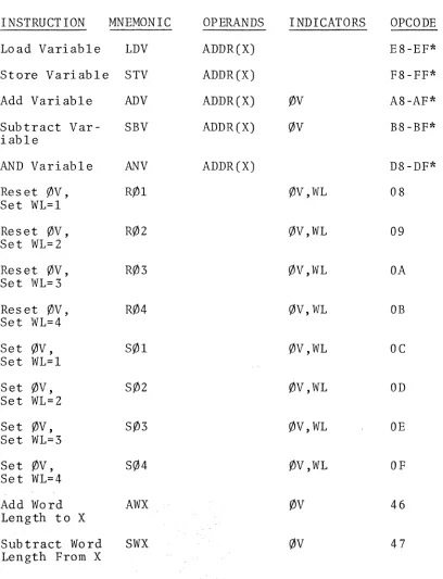
3.3 Variable Word Length Instructions
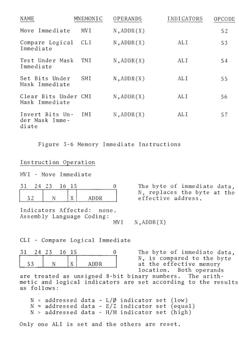
3.4 Memory Immediate Instructions
3.5 Memory to Memory Instructions
3.6 Transfer of Control Instructions
3.7 Control Instructions
3.8 Input/Output Instructions
4.0 COMPUTER OPERATION
4.1 Front Panel
4.2 Basic Panel Operation
4.3 System Panel Operation
4.4 Bootstrap Loader
4.5 Disk IPL Option
4
6
6
9
15
19
21
24
27
27
41
47
56
60
81
90
95
104
104
105
109
114
[
[
[
[
['
[
[
(~
[
[
[
l:
I:
r
[
[
I
[
[
A.
B.
C.
D.
E.
F.
G.
H.
1.
-3-APPENDIXES
Instructions Listed Numerically by Opcode
Instructions Listed Alphabetically
Instruction Execution Times
Power Fail/Auto Restart Programming
DMA Channel Programming
Firmware Extension Procedures
Instruction Flowcharts
Dedicated Memory Locations
Internal Codes
117
122
127
133
135
138
142
147
1.0
-4-INTRODUCTION
The CIP/2200 is a general purpose byte oriented mlnl-computer designed primarily for dedicated system applica-tions. The CIP/2200 has an extensive instruction set including binary and decimal arithmetic capability, character string and bit manipulation instructions.
The CIP/2200 has an 8 bit hardware data path and memory. The CPU registers, however are 16 bits in length. The instruction set includes a complete set of 16 bit register to memory and register to register binary arithmetic
instructions. In addition to the 16 bit word instructions, the CIP/2200 includes a variable length binary arithmetic capability, allowing binary arithmetic to be performed on 8, 16, 24, or 32 bit data without resorting to multiple precision software routines. A third group of instructions provides memory to memory decimal arithmetic on ANSCII
format character strings up to 16 digits in length. Other memory to memory operations include character string move and compare, code conversion, and decimal editing.
Main memory consists of 8 bit/byte or 9 bit/byte core memory with a 1.1 microsecond full cycle time, Memory is expandable in 8k byte modules from a minimum of 8k bytes to a maximum memory size of 32k bytes. Memory parity protection is available as an option on systems with 9 bit/byte memory.
The CIP/2200 I/O structure consists of a microprogrammed serial I/O interface, a byte I/O facility, firmware
supported Direct Memory Channel concurrent transfers, and the capability of attaching up to two independent Direct Memory Access (DMA) processors. The serial I/O interface is a microprogram for controlling serial data transfers,normally used to control a teletype or other similar terminal device. The byte I/O
facility is us~d for transmission of 8 bit data between anyone of up to 32 peripheral devices and either an
accumulator register or main memory under program control. Associated with the byte I/O facility is the external
priority interrupt system. The CIP/2200 has a capacity for up to 64 external priority interrupts. Byte I/O interfaces normally contain the logic for data transfer related interrupts. Non device-related interrupts may be added in groups of 8 for a total of 64 interrupts.
111. t!j
~
: , , , :~
[:
[
[
[
[
[
r
I'
[
I
[
[
I
I
-5-The Direct Memory Channel feature (DMC) allows micro-program controlled, high speed data transfer to occur
concurrently with program execution. The maximum DMC transfer rate is 86,000 bytes per second for asynchronous devices and 25,000 bytes per second for synchronous
devices. Requirements for faster operation (up to
910,000 bytes per second) may be filled with a hardware Direct Memory Access processor. The Direct Memory
Access unit is an independent hardware controller which competes with the CPU for use of main memory time.
The CIP/2200 is a microprogrammed general purpose mini-computer based on the CIP/2000 Computer. The use of
microprogramming has allowed instructions of considerable power and flexibility to be implemented at modest cost. Microprogramming offers the user the added power of
features such as a bootstrap loader, an integral serial I/O facility, a high speed Direct Memory Channel, and complex ins tructions such as "Edi t and Mark" and
.0
.1
-6-GENERAL CHARACTERISTICS
Basic Machine Architecture
Registers
The CIP/2200 has three programmable registers, the accumulator (A), the accumulator extension (B), and the index register (X). Two other registers, the pro-gram counter (P) and the status register (S) are also of importance to the programmer.
The A register is the 16 bit main accumulator register. It is an operand source for all binary arithmetic and logical instructions, and receives the result of all binary operations except store. Serial and byte mode
I/O operations may transfer data to or from the low 8 bits of the A register.
The B register is also 16 bits in length and serves as an accumulator extension for variable length binary arithmetic and logical operations. Byte mode I/O opera-tions may transfer data to or from the low 8 bits of the B regis ter.
The index register (X) is a 16 bit register used for address modification and base relative addressing. Several specialized instructions are provided for index value modification.
The P register (program counter) contains the address of the next machine instruction to be executed. The
P register contents are stored by the subroutine transfer instruction (RTJ) and are altered by transfer of control instructions (jump, skips, etc.). When an instruction modifies the P register contents, the address of the next machine instruction to be executed is determined by the contents of the P register after it has been modified.
The status register (S) is an 8 bit register containing the CIP/2200 internal status indicators. The indicators are stored as shown in the illustration below. The meaning of each indicator is described in Figure 2-1.
_ _ _ _ _ _ _ _ _ _ _ _ _ _ _ _ _ _ .~_~.u __ ~· ~ .. _ _ _ _
rI'1
~
\fl.
iJ
[
r:
I)
11
I~
[
[
[
I
I
7
PF
MNEMONIC
PF
E/ Z
L/'/J H/M INT '/JV WL
6 5
E/Z L/ '/J
Figure 2-1.
Power Failure (PF)
-7-4 3 2 1
a
H/M INT '/JV WL
NAME
Power Failure Indicator
Equal/Zeros Result Indicator Low/Ones Result Indicator High/Mixed Result Indicator
Interrupt System Disabled Indicator Overflow Indicator
Word Length Indicator
CIP/2200 Status Register
The power failure indicator reports the status of the computer's electrical power supply. The power fai1/ automatic restart option monitors the power supply and generates an internal interrupt whenever the input power line voltage becomes insufficient for reliable operation. The firmware detects the interrupt, sets the power failure indicator, and causes the CIP/2200 program to transfer to a user programmed power failure interrupt service routine. When normal power supply voltage is restored, the power
fail/automatic restart option causes another internal interrupt. The firmware, in response to the power restart indication, resets the power failure indicator and trans-fers to the user written power restart routine. If the power fail/automatic restart option is not installed, the power failure indicator is set to zero by a RESET and is not changed by the hardware.
Arithmetic and Logical Indicators (E/Z, L/'/J, H/M)
The indicators represented by bits 4-6 of the status register are collectively called the arithmetic and logical indicators (ALI). These three bits are used to save information about the results of the memory to memory and memory immediate arithmetic and logical
-8-The "E/Z" (Equal/Zeros result) indicator is set when
the operands of a compare are equal or when the result of an arithmetic or logical operation is zero. The "L/¢"
(Low/Ones result) indicator is set when the source of a compare is lower (more negative) than the target, when the result of an arithmetic operation is negative, or when the result of a logical operation contains all ones. The
"H/M" (High/Mixed result) indicator is set when the source of a compare is higher (more positive) than the target, when the result of an arithmetic operation is positive, or when the result of a logical operation contains mixed ones and zeros.
The meaning of the individual indicators depends upon the type of operation which caused ~hem to be set. For example, an arithmetic operation which produces a negative (low)re-suIt will cause bit 5, the Low/Ones indicator, to be set. Similarly, a logical operation which causes all bits of the result to be ones will also set the Low/Ones indicator. Note that the arithmetic and logical indicators are set
only by the memory to memory and memory immediate instructions and are not altered by binary arithmetic and logical
in-structions. The indicators may be tested with a conditional branch instruction; testing does not cause the indicators to be reset.
Interrupt System Disabled Indicator (INT)
The INT indicator reports the external interrupt system status. The INT indicator is zero when external interrupts are enabled and one when they are disabled or masked. The INT indicator is meaningless in systems which do not have the interrupt enable/disable option installed.
Overflow Indicator (¢V)
The overflow indicator is set when an arithmetic overflow is detected during a binary or decimal arithmetic operation. The overflow indicator may be tested and reset by conditional skip instructions or tested without resetting by a
condi-tional branch instruction. Instructions are also provided to set and reset the overflow indicator without testing.
The overflow indicator is not reset by binary arithmetic operations. Thus, an overflow test over multiple binary operations may be achieved by resetting the indicator before
[
[
[
I
[
[
[
I
[
[
(;
[
[
r
[
[
I
[
[
(
[
I
I
[
2.2
-9-the sequence of instructions to be tested and testing after the last operation. If one or more of the in-structions caused an overflow, the indicator will be set.
An arithmetic overflow occurs when the result of an operation is too large to be contained in the receiving field or register. For decimal operations this occurs whenever the target field is shorter than the source
field, or when a carry occurs when operating on the left-most target digit. For example, when 10 is added to 995 in a three digit field, an overflow occurs. A binary over-flow occurs whenever the result of the operation is too large to be contained by the receiving register. This condition is detected by comparing the carry into and out of the sign bit (left-most bit) of the register; if these carries are not the same an overflow has occurred.
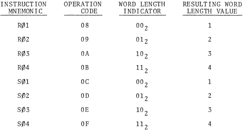
Word Length Indicator (WL)
The word length indicator defines the word length currently in effect for variable length binary operations. Variable length data may be from 1-4 bytes long. Values of 002 to 112 in the two bit word length indicator correspond to variable data sizes of 1 to 4 bytes, respectively. The word length value is set programmatically with control
instructions. A system reset causes the word length to be set to 1 byte (WL
=
002) •System Save Area
The system save area is a 16 byte area of memory reserved for use by the CIP/2200 firmware. The system save area is located immediately after the external interrupt loca~
tions, from IB016 to IBF16.
Information Formats
The B bit byte is the basic data element from which all data, addresses, and instructions are formed. The bits within the byte are numbered from -7 to 0 from left to right.
An optional 9th bit may be added to each byte in memory to provide a memory parity check. This 9th bit is used only to detect memory malfunctions and is set, reset,
-10-Three basic types of information are used by the CIP/2200: data, addresses, and instructions. Data are items of information acted upon by the computer as directed by the program, and may have several forms. Addresses are informa-tion items containing the locainforma-tion of other items in memory. An address may be either part of an instruction or a
separate item. In the latter case, the address is often referred to as a "pointer" since the address "points
to" the location of some other item. Instructions are the information items which control the action of the computer.
Data Formats
Data may be stored and processed in several forms by the CIP/2200. The form chosen depends upon the nature of the data and the operations to be performed. Numerical data may be represented in either 2's complement notation binary (base 2) or sign and magnitude notation decimal
(base 10) form. Logical data are represented as unsigned binary items. Alphanumeric data (text) are represented as strings of bytes, each byte being the ANSCII code for a single character.
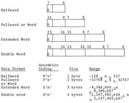
7 0
Halfword
Is
I I
15 8 7 0
Ful1word or Word
Is I
I
I
23 16 15 8 7 0
Extended Word
Is
I
I
I
I
31 24 23 16 15 8 7 0
Double Word
6
I
I
I
I
I
Assembler
Data Format Coding Size Range
Ha1fword H'n' 1 byte -128 n $.. 127 Fu1lword F'n' 2 bytes -3276t $.. n $.. 32767
or Word
Extended Word E'n' 3 bytes -8,388,608 <n
..$.
8,388,607-Double word DIn' 4 bytes -2,147,483,648 < n <
2,147,483,647-Figure 2-2 Binary Data
. - - _ ..
---~---I
I
if!
IjIf
[image:14.612.78.498.379.716.2][
I
(
", ,
J
[
,[
,
[
[
[
[
I [
I
[
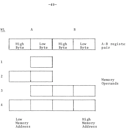
-11-Binary data may be stored and processed in either 2 byte (16 bit) words or in variable length byte strings up to 4 bytes (32 bits) in length. The address of a data item is the address of the leftmost (most significant) byte. The lower order bytes occupy higher addressed bytes in memory. The various binary data formats, the range of values representable in each format, and the assembly language specification for each are shown in Figure 2-2.
Decimal numbers are represented within the CIP/2200 as strings of ANSCII decimal digit characters in memory. Decimal numbers may vary in length from 1 to 16 digits. Each digit is represented in memory as one byte contain-ing an ANSCII zoned decimal digit. The low four bits
(bits 3-0) of the byte contain the binary equivalent of the decimal digit. The high four bits (bits 7-4, the zone bits) of a decimal operand digit contain the ANSCII decimal digit zone, 10112, with the exception of the low order digit (highest addressed byte) of a decimal number. The zone bits of the low order digit of a number contain the sign of the decimal number. A minus sign is represented by zeros in the zone of the low order bits; a plus sign by a zone of 1011 2 (B16)'
The illustration in Figure 2-3 shows typical decimal numbers as they appear in memory. The leftmost byte is the addressed byte; the remainder of the number occupies successively higher locations in memory.
Assembler Coding Machine Representation (hex)
Z'123456'
Z' -0123456' B 0 B 2 B 4 B 5
Sign
=12=
Logical data is represented as either 2 byte words or variable length byte strings of from 1 to 4 bytes. The representation is similar to binary data, except that logical data is unsigned.
Alphanumeric data (text) and other character string data are represented in the CIP/2200 as variable length byte strings in memory. The individual bytes are treated as unsigned 8 bit logical items. Byte strings of from one to 256 bytes may be operated upon by memory to memory instructions. The standard internal code used by the
CIP/2200 is ANSCII with bit 7 set to a 1 (See Appendix I), but other codes (e.g., EBCDIC) may be used as desired by the programmer. The CIP/2200 CPU is insensitive to the choice of code except for decimal number representation and certain characters used for editing. I/O devices and system software, however, are code sensitive and usually require ANSCII code.
Addresses are represented in several forms within the various instructions. Addresses not part of an instruc-tion (pointers) are always represented in memory as 2 byte words as shown below. The memory address appears as
15 8 7
o
a 15 bit positive integer in bits 14-0 of the address word;an address word can therefore address 32,768
different bytes. Since negative addresses are not used, the sign bit (bit 15) of an address is always zero and is not
needed. The sign bit of an address word is therefore avail-able to specify indexing. A 1 in bit 15 of an address
word in memory is used to indicate that the effective address is the sum of the index register contents and the address contained in bits 14-0 of the address word. If bit 15 is a 0, the effective address is s imply the value stored in bits 14-0 of the address word.
Instructions
CIP/2200 instructions vary in length from one to eight bytes depending upon the number of memory addresses
required, the addressing modes specified, and the other information contained in the instruction. Variable instruction length permits efficient utilization of
memory while permitting a wide range of instruction types.
- - - " " - - -
-[
[
[
(
[
[
[
[
[
[
[
[
[
[
[
I
[
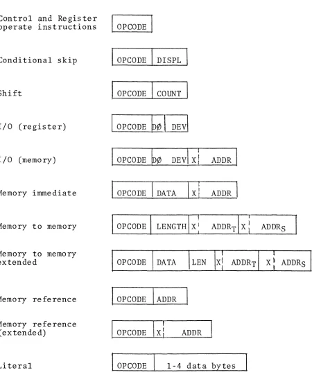
-13-In all cases the first byte of the instruction contains a code indicating the operation to be performed. The second byte of less frequently used instructions contains an
extended operation code. The basic instruction formats are shown in Figure 2-4.
The control and register operate instructions do not refer to memory and consist of a one or two byte operation code only. Conditional skip instructions allow the program to test various machine conditions and alter the execution path of the program depending upon the result. Conditional skips have a one byte displacement address allowing control to be transferred to instructions within + 128 bytes of the conditional skip. Shift instructions also use the two
byte format; the first byte contains the operation and the second byte contains the count of bit positions to be
shifted. Input and output (I/O) instructions require either two bytes (for transfers to or from a register) or four bytes (for transfers to or from memory). Memory immediate instructions occupy four bytes and provide
various operations between a data byte in the instruction itself and a byte in memory. The memory to memory format is used for decimal arithmetic and byte string operations.
The memory reference, extended memory reference, and literal formats are used by most binary arithmetic, logical, and transfer of control instructions. Eight addressing modes allow considerable flexibility and power while conserving memory.
The CIP/2200 provides a control stack mechanism to aid the programmer in saving the machine state when entering subroutines or interrupt service routines. The machine state saved on the stack by the save instruction con-sists of the contents of the program counter (P), the
machine status register (S), and the B, A, and X registers as shown below.
P S B A X
---~~ - - -.. ~~---.---~-- - - -.. ---
~---Control and Register operate instructions
Conditional skip
Shift
I/a (register)
I/a (memory)
Memory immediate
Memory to memory
Memory to memory extended
Memory reference
Memory reference (extended)
Literal
-14-I
apcaDEI
I
apcaDEI
DISPLI
apcaDEI
caUNTI
apcaDEb~1
DEV\I
apcaDE~~
DEV\xl ADDRI
I
apcaDEI
DATAI
xl ADDRI
I
apcaDEI
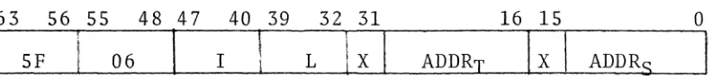
LENGTH\X: ADDRT\X; ADDRSI
apcaDEI
DATA ILENIx:
AlJDRTIxl
ADDRS~
apcaDEI
ADDRI
apcaDEI
xl ADDRI
apcaDE 1-4 data bytes Figure 2-4 CIP/2200 Instruction Formats~
~
[
~
~
~
[
I
I
~
~
~
I
I
I
I
I
I
[image:18.612.87.537.124.668.2]I [
[
[
[
I
[
[
[
[
[
I
I
[
2.3
-15-Memory Addressing
The CIP/2200 has the capability of addressing up to 32,768 bytes of memory. The basic addressing mode, extended
addressing, utilizes a 16 bit address word. The low 15 bits contain the binary value of the address. Bit 15 is used to request indexing. Indexing may be specified for any memory reference using extended addressing. A single
15 8 7
o
level of indirect addressing is provided for certain memory ref-erencing instructions. When in-direct addressing is used, the address word specified by the instruction may be indexed.
In addition to extended addressing, many memory reference type instructions have seven other addressing modes, for a total of eight modes. These additional addressing modes
include various short (1 byte) address types, literal address ing, and indirect addressing. The low three bits of the
operation code byte of these instructions contain a three bit addressing mode, m, as shown below. The remainder of
7 320
I
OPCODEt mI
the instruction consists of from zero to four bytes depending on the addressing mode selected. The operation specified in bits 3-7 of the instruction is perform-ed on the data locatperform-ed at the effective address (EA) , the memory location specified by the result of the indicated address computation.
The individual addressing modes are discussed in the follow-ing paragraphs. Modes 2 and 3, (and mode 7 for JMP and RTJ) specify indirect addressing. In all three cases the effec-tive address is the location specified by an address word. The effective address is the contents of bits 14-0 of the address word if bit 15 is O. A one in bit 15 causes the
15 8 7
o
address specified by bits 14-0 of the address pointer to be modified by addition of the contents of the
index register.
Direct page 0 (m=O) EA = ADDR
15 11 10 8 7
I
OPCODEI
0 0 0I
ADDRo
The effective address is given by the second byte of the instruction. This mode allows a short, fast means for accessing data in the first 256 locations in memory. Direct page zero addressing is commonly used for sharing data between programs. Considerable savings in program size can result from placing commonly used data
-16-Direct relative (m=l) EA = (P) + DISPL 15 11 10 8 7 6
I
OPCODEI
0 0 0I
SI
DISPLo
The effective address is given by the sum of the program counter CP) and the 2's complement eight bit displacement contained in the second byte of the instruction. The program counter contains the address of the first byte of the next instruction when the address computation is performed. A displacement of zero, therefore, addresses the next instruction. This mode provides a sav-ings in memory required when addressing the 256 byte area of memory around the current instruction, from 127 bytes ahead to 128 bytes behind the first byte of the next instruc-tion. Since programs tend to refer most frequently to near-by locations, this mode allows considerable economy ofstorage. Note that this mode is identical to the addressing mode of the conditional skip instructions.
Indirect page 0 Cm=2) EA = CADDR)
15 11 10 8 7
o
I
OPCODEI
0 1 0I
ADDRThe second byte of mode 2 instructions contains an 8 bit absolute address specifying a location in page zero. The two byte address word at the specified
location is used to obtain the effective address as explain-ed above for indirect addressing. Indexing may be specified by the indirect address word. This mode provides a
con-venient means of using shared address pointers,
Programming Note: A series of page zero pointers (a transfer vector) may be used to provide dynamically al terab Ie linkage between subroutines.
Indirect relative (m=3) EA = (CP) + DISPL) 15 11 10 8 7 6
DISPL
o
The sum of the contents of the program counter and the 8 bit 2's complement dis-placement gives the address of an address word. The address word is evaluated to form the effective address. This mode provides a means of shar-ing address words located within a section of a program. Indirect relative addressing also provides a means of re-turning from a subroutine by an indirect jump.l r : . "
i;
~I
I
[
~
Ii
Ii
I
[
[
[
[
[
[
[
[
[
[
[
-17-Programming Note: Indirect relative addressing can be
used to save memory by sharing address words when multiple instructions located close together refer to a distant
location. One reference is made to the desired datum using
extended addressing (mode 6). All other references within
relative range can be made indirect relative using the ex-tended address word portion of the mode 6 instruction as a pointer.
Base addressing (m=4) EA = (X)
7 3 2
I
OPCODE\l 0 01o
This mode provides a fast, one byteinstruction format. The effective
address is the contents of the index
register (X). Mode 4 addressing is
particularly useful for string processing or table pro-cassing where the index register is used to point to the byte in the string or entry in the table currently being processed.
Base plus displacement addressing (m=5) EA = (X) + DISPL
15 11 10 8 7
I
OPCODE 11 0 11 DISPLo
The effective address isgiven by the sum of the contents of the index register and the 8 bit unsigned displacement contained in the second byte of the
instruction. This mode may be regarded as an indexed page
zero address (for page zero data tables) or as a base plus displacement mode where the index register contains the address of the datum.
Extended addressing (m=6) EA = ADDR or ADDR + eX)
23 19 18 16 15
I
OPCODEll 10lxI ADDRo
This mode isthe basic addressing mode discussed
in the beginning of this section. If indexing is not
spec-ified, the effective address is contained in the low 15 bits
of the second and third bytes of the instruction. If
index-ing is specified, the effective address is the sum of the
contents of the ADDR field and the index register. This
-18-Literal addressing (m=7) EA = 2nd byte of instruction
OPCODE 1 1 11 DATA (1-4 bytes)
Literal addressing provides a means of cod-ing data in the instruction itself, thus savcod-ing the memory otherwise required to specify the address of the data. The length of the data may vary from one to four bytes de-pending upon the requirements of the opcode.
Extended indirect addressing (m=7, jump and return jump only) EA
=
(ADDR or ADDR + (X))I
OPCODE 1 1 1Ixi
ADDRThe address word located
in the second and third bytes of the instruction is evaluated as described for mode 6. The result specifies the location of an address word, which is evaluated to form the effective address of the
instruction. This mode is provided in lieu of literal addressing for the jump and return jump (subroutine trans-fer) instructions. Extended indirect addressing provides a means of utilizing transfer vectors (jump tables) outside of page zero.
The assembly language coding of the various addressing modes is shown below.
OPC ADDR modes 0,1 (direct page zero and direct relative)
OPC* ADDR modes 2,3 (indirect page zero and in-direct relative)
OPC- mode 4 (base addressing)
OPC+ N mode 5 (base plus displacement) OPC/ ADDR(X) mode 6 (extended addressing) OPC= DATA mode 7 (literal addressing)
OPC= ADDR(X) mode 7 (extended indirect addressing for JMP and RTJ only)
Figure 2-5 Address Mode Assembly Language Coding
I
I
-[
[
[
[
[
[
[
[
[
[
[
[
[
[
[
I
[
2.4
-19-Interrupt Structure
Basic Interrupt Action
The CIP/2200 interrupt system is responsive to two types of interrupts. Internal interrupts are generated by the computer on the occurrence of an operational fault, a console interrupt, or by the interval timer. External interrutts are generated by an I/O device or another externa ly supplied signal. Each interrupt is assigned an address word in main memory called an interrupt trans-fer location. These assignments are shown in Fig. 2-6.
The interrupt transfer location specifies the address of a software routine which will be executed whenever the associated interrupt is recognized. When an interrupt occurs, the computer responds by executing a subroutine transfer of control to the address specified by the
interrupt transfer location. This mechanism for interrupt-ing the execution of one program and startinterrupt-ing execution of another program allows the computer to respond to external events and execute the appropriate portions of the program on a priority basis.
Location
080-081 082-083 086-087 08A-08B 08C-08D 08E-08F 090-091 100-101 102-103
l7E-l7F
Figure 2-6
Assignment
Console Interrupt DMA Channel Interrupt Interval Timer Interrupt
Memory Parity Error Interrupt
Control Stack Under/Overflow Interrup' Power Fail Interrupt
Power Restart Interrupt External Interrupt 0 External Interrupt 1
External Interrupt 63
-20-Internal Interrupts
The internal interrupts are used to report computer opera-tion faults or the occurrence of events with a high pri-ority. Internal interrupts are generated by the console interrupt switch or a trap instruction, the DMA channel, the interval timer, the memory parity option hardware, a control stack under/overflow, and the power fail/restart option hardware.
The console interrupt is generated by depressing the con-sole interrupt switch on the computer front panel or by executing a trap instruction.
The DMA channel interrupt is genera ted by the DMA pro-cessor at the end of a DMA transfer. If a system has more than one DMA processor, both interrupts will occur through the same interrupt transfer location. A status check on one of the DMA processors must be used to determine which one interrupted. For details of operation of the DMA
channel, refer to the DMA processor manual and Appendix E.
The interval timer interrupt occurs when the interval timer counter value reaches zero. The interval timer counter in memory locations 84 - 8516 is incremented by the interval timer (real time clock) option on the processor option board. The rate at which the timer is incremented is selected by jumpers on the processor option board. The board is supplied with the jumpers set for a I millisecond interval, but other intervals may be obtained by spap.ging the jumpers as described in
thef:roces:so:r OptioJ!/B:o~rd Manual (publication #7 000 0052MA).
TheEI't'an~DIT' .iilstl:'tictions are used to start and stop
tlH~t;p:'t:.e. I:val timeT.. . '.' .'
~.'
. th~':ni~mory parity failtite interrupt occurs when a pari ty '. failure (an odd number of bits in a byte) is detected
.. by the memory pari ty check option hardware. The memory parity check option cC)J)sists of a 9 bit memory and the parity check optionori:,:the processor option board.
If the memory parityqheck option is not supplied, the interrupt will notbe:\'generated.
The control
stacklln,~er/overflow
interrupt is caused when the control stack .¢~n.not hold or supply sufficient data. This interrupt can only occur as a result of execution of a save or return instruction (SAV, RET, or RTN; see Section 2.6).[
[
Ifr
IJ
I_
, i ii
I
[
I
I
[
[
[
[
[
[
[
I
(
I
[
[
[
I
I
2.5
-21-The power failure interrupt occurs when the primary power supply voltage becomes insufficient for reliable computer operation. The power restart interrupt occurs when the power supply is restored to the computer after a power failure. Certain requirements must be met by the power failure interrupt service routine if the contents of memory and the machine state are to be preserved. Refer
to Appendix A for notes on the design of this program. The power fail and automatic restart interrupts are set by the power fail/automatic restart option on the processor option board, and will not occur unless that option is
installed.
External Interrupts
External interrupts may be generated by I/O device con~
trollers or other external hardware devices. The CIP/2200 has provision for a total of 64 external interrupts. The external interrupt system may be disabled (masked) to defer recognition of interrupt requests if the interrupt enable/disable option is installed.
Input/Output Facilities
The CIP/2200 provides four basic types of I/O transfers ranging from bit serial transfers at 10 characters per second to Direct Memory Access (DMA) byte transfers at 910,000 bytes per second. The serial I/O facility is a low speed interface suitable for operating a low speed terminal device. Byte I/O provides either program loop or interrupt I/O capabilities for medium speed devices. The Direct Memory Channel (concurrent I/O) facility pro-vides a firmware managed high speed data transfer at a rate of up to 86,000 bytes per second concurrent with
and transparent to normal program execution. Direct Memory Access I/O utilizes a separate hardware channel into memory to provide extremely fast I/O at the maximum memory rate of 910,000 bytes per second.
Serial I/O
The serial I/O interface provides a simple, inexpensive means for communicating with a teletype or other similar
terminal device. The serial I/O interface is a micro-program which controls the transfer of bit serial data between the computer and a serial I/O device. Serial
-22-Byte I/O
The CIP/2200 byte I/O facility provides for program con-trolled data transfers over the byte I/O bus. Each byte of data transferred to or from an I/O device controller requires the execution of an I/O instruction. The byte I/O bus is also used to transfer status information from devices to the computer and to transmit function bytes containing control information to the devices. The byte I/O facility is related to the external interrupt facility in that device controllers are able to cause an interrupt when ready for a data transfer or when an error is detected. The interrupt service routine then uses the byte I/O instruc-tions to test the device status and to take appropriate
action. This allows I/O transfers to be overlapped with background (non-interrupt) program execution.
The byte I/O facility may also be used without interrupts by testing the device status continually until the device is found to be ready to accept or send data. The upper limit of the byte I/O transfer rate is approximately 10,000 bytes per second.
The byte I/O facility offers considerable flexibility to the programmer. Data and status or control informa-tion can be transferred between external devices and the A or B register or memory. Up to 32 device controllers may be connected to the byte I/O bus.
Direct Memory Channel (DMC)
The Direct Memory Channel (concurrent I/O) facility allows automatic block data transfers between devices attached to the byte I/O bus and memory. DMC transfers are firmware controlled and occur concurrently with normal program execution.
Concurrent operation of I/O and program execution is accomplished by assigning higher priority to DMC data transfers than to instruction execution. Before each instruction is executed, a firmware check is made for pending DMC transfers. All such data transfers for DMC operations are finished before an instruction is executed. A DMC transfer may also force short breaks in the
execu-tion of long instrucexecu-tions.
11.'.
~
[
11.'
Ij
[
[
[
I
[
[
[
[
I
[
[
[
[
i [
[
[
-23-The maximum rate at which DMC transfers can occur is deter-mined by the time between the arrival of a data transfer request and the servicing of that request by the micro-program. The microprogram tests for pending DMC requests at discrete intervals. The longest interval possible between the occurrence of a DMC transfer request by the highest priority DMC controller and the answering data
transfer is 40 microseconds. The CIP/2200 can therefore support a 25,000 byte/second transfer rate for a single synchronous device. (A synchronous device is a device which requires data transfers at a fixed rate determined by the device itself, for example, a magnetic tape drive.) When multiple devices are simultaneously transferring
data, the maximum time between a request and the transfer is 40 microseconds for the highest priority device, 52 microseconds for the second highest priority device 64 microseconds for the third highest priority device, and so on. The maximum aggregate data transfer rate for the DMC channel is approximately 86,000 bytes/second. This rate can be maintained only if requests arrive at less than 12 microsecond intervals. Since service for these requests can only be guaranteed at a rate of 25,000
bytes/second, rates of more than 25,000 bytes/second can only be supported on asynchronous devices (devices with variable transfer rate, i.e., devices which can operate
at rates slower than the maximum such as a tape perforator).
The location and amount of data transferred during a DMC block transfer operation is determined by a four byte DMC descriptor. A two word (4 byte) dedicated page zero loca-tion is reserved for the DMC descriptor for each I/O
device. The address of this descriptor is calculated by multiplying the device number by 4. The descriptor
contains two address words, a current address and an ending address. The current address word contains the address of the next byte to be transferred by the I/O operation. The ending address word contains the address of the last byte to be transferred. The current address is incremented after each byte transfer. When the current address becomes greater than the ending address, the DMC operation is terminated.
DMC operations are started by initializing the descriptor and executing the appropriate byte I/O instruction. After a DMC I/O operation is initiated by a processor instruction, byte transfers proceed automatically until the last byte of
• 6
-24-is twice the device address plus 10016' If termination without an interrupt is desired, the program must check the device status word to determine the state of the DMC transfer.
DMA Operations
The DMA processor may be used for high speed data transfer directly to memory at a maximum rate of 910,000 bytes per second. The DMA processor is an independent hardware device which is attached directly to the main memory address, data, and control busses. Data transfers per-formed by the DMA processor are completely independent from operation of the main computer except that both devices use the same memory. The DMA processor takes precedence over the CIP/2200 CPU for memory operations.
Programming for DMA transfers is described in Appendix E .
Control Stack Facility
The CIP/2200 control stack facility provides a method for saving and restoring the computer state information. The implementation of state switching using a control stack greatly increases programming ease and flexibility, partic-ularly in an interrupt environment.
Computer State Information
The computer state information uniquely defines the internal state of the computer at a given point in a program. The CIP/2200 state information consists of the contents of the A, B, and X registers, the location of the next instruction to be executed (P), and all status indicators (S). This information is reloaded into the computer registers when the machine state is restored. The machine state must be saved by a subroutine or an interrupt service routine to
allow the programmer to use registers, change word length, or alter other status indicators freely in the subroutine or interrupt service routine without affecting the values stored in the computer registers during the execution of other programs. State saving is essential for interrupt service routines since the interrupted program must be
able to continue as before when the interrupt service routine returns.
~-~-~---
-lli
(Ij
~
[
[
[
[
:1
[
I
[
(
[
[
[
[
[
(
[
I
[
[
I
[
-25-Stack Operations
A stack is a data storage element containing a varying number of entries. Data is entered and removed from the stack in a Last In-First Out ("LIF0") manner. LIFflJ
operation means that when data is removed from the stack, the information removed first is that which was entered into the stack most recently. Entry of data into a stack is called "push ing" and data removal is known as "popping".
Control Stack Use
The control stack is used to save the computer state. Each entry in the CIP/2200 control stack consists of a complete set of state information. The most recently saved machine state is on the "top" of the stack, the oldest machine state on the "bottom". In normal use
each subroutine saves the machine state immediately after being called. The subroutine returns the state information by using the RET or RTN instruction to "pop" the old machine state from the stack. When multi-level subroutine calls are used, the control stack will contain more than one entry during execution of the lower level subroutines. As each subroutine terminates, one more entry is removed from the stack. When control returns to the original
calling routine, the control stack will be empty. Uniform use of a save and restore convention greatly enhances the reliability of programs, especially in an interrupt
environment.
Control stack operations are performed by the SAY, RET, and RTN instructions. The location of the control stack is defined by the control stack pointer which occupies a dedicated page zero location - 92 - 9316. The control stack pointer always contains the address of the first
(lowest addressed) byte of the most recently stacked machine state information. The control stack occupies
-26-The length of the control stack area used by a program is determined by the number of levels of subroutines and interrupts allowed. For example, a program having a four level subroutine structure (where at most four sub-routines are simultaneously in use - A calls B which
calls C which calls D) requires 36 bytes for its con-trol stack (9 bytes per SAY) regardless of the total number of subroutines in the program. Additional con-trol stack space must be reserved for interrupt pro-cessing because interrupts can, in general, occur at any time. Each interrupt requires a minimum of 9 additional bytes of reserved control stack space. Interrupt service routines may also require further control stack space for subroutines.
I
[
•
IJ
[
I
I
[
[
[
[
[
[
[
[
[
[
I
[
I
,
3.0
3.1
-27-MACHINE INSTRUCTIONS
This section describes the operation of the CIP/2200
machine instructions. The instructions are grouped by
logical type into several subsections. Details of
memory addressing are given in section 2.3 and are not
repeated for each instruction. The instruction
descrip-tions include the format of the instruction as it appears in memory and the CIP/2200 assembly language coding.
An asterisk to the right of the machine instruction for-mat diagram indicates that the eight addressing modes
discussed in section 2.3 apply. The assembly language
coding for those cases assumes extended addressing (mode 6).
The abbreviations used in this chapter are shown below.
ALI Arithmetic and logical indicators
E/Z Equal/zero indicator
L/0 Low/ones indicator
H/M High/mixed indicator
INT Interrupt system disabled indicator
0V Arithmetic overflow indicator
WL Word length indicator
PF Power fail indicator
A A register (accumulator)
B B register (extended accumulator)
X Index register
P Program counter
Binary Arithmetic and Logical Instructions
The instructions in the binary arithmetic and logical instruction group perform binary arithmetic operations on fixed length 16 bit 2's complement numbers or perform logical
operations on 16 bit unsigned binary data. In general, one
operand resides in a register, usually the A register, and the
other is in memory. Instructions are provided for moving
data between registers; transferring data between registers and memory; and for adding, subtracting, counting, masking,
and inverting 16 bit data. Special instructions are
-28-Binary arithmetic is provided both for general computation and for address and index computation. Since the binary arithmetic operand length is consistent with the CIP/2200 address word size, the full arithmetic and logical capabil-ities of the instruction set may be used for address
computation.
The two fixed length binary data formats are shown below. Some of the instructions in this group also use 8 bit immediate data. When a shorter field is added to a 16 bit integer the sign of the short field is extended to provide 16 data bits. Note that when zero is complemented
in 2's complement notation no change occurs.
15 0
I
s
I
INTEGERI
arithmetic data15 0
I
DATAI
logical dataThe results of all arithmetic instructions are tested for an overflow (result greater than 215 _1 or less than -2 15 ). The overflow indicator is set if an over-flow occurs but it remains unchanged if no overover-flow occurs.
Instructions in the variable length arithmetic group (Section 3.3) and in the shift group (Section 3.2) supplement the fixed length arithmetic and logical capabilities of the CIP/2200. When mixing fixed and variable length instructions, care must be taken to ensure that the registers are used consistently.
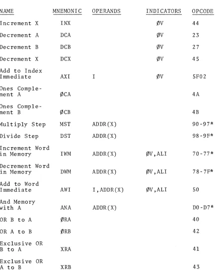
The binary arithmetic and logical instruction group is shown in Figure 3-1. The table lists the name, the assembler mnemonic, the operands in assembler notation, the indicators affected, and the machine operation code in hexadecimal notation. Those instructions allowing eight addressing modes are indicated by an asterisk following the operation code.
-I
[
I
I
I
[
-29-I
[
I
NAME Load A MNEMONIC LDA OPERANDS ADDR(X) INDICATORS OPCODE EO-E7*[
Load B LDB ADDR(X) CO-C7*Load X LDX ADDR(X) 80 - 8 7*
[
Store A STA ADDR(X) FO-F7*[
Store B Store X STB STX ADDR(X) ADDR(X) C8-CF* 88-8F*[
Transfer Ato B TAB 2B
I
Transfer B to A TBA 2FI
Transfer A to X TAX 4CTransfer X
I
to A TXA 4ETransfer B
[
to X TBX 4DTransfer X
I
to B In t e rch an ge TXB 4FA and B lAB 03
[
InterchangeA and X lAX 35
[
InterchangeB and X IBX 36
I
Add to A ADA ADDR(X) ~V AO-A7*Subtract
OV
[
from A SBA ADDR(X) BO-B7*A INA rfJv 48 Increment
I
Increment B INB f/Jv 49-30-
II
[
I
NAME MNEMONIC OPERANDS INDICATORS OPCODE[
Increment X INX
'IN
44Decrement A DCA '/JV 23
I
Decrement B DCB '/JV 27
Decrement X DCX '/JV 45
I
Add to Index
[
Immediate AXI I C/JV 5F02
Ones
Comp1e-[
ment A '/JCA 4A
Ones
Comple-ment B '/JCB 4B
~
, \
Multiply Step MST ADDReX) 90-97*
Divide Step DST ADDReX) 98-9F*
~
Increment Word
in Memory IWM ADDReX) C/JV,ALI 70-77*
~
Decrement Word
in Memory DWM ADDReX) C/JV,ALI 78-7F*
I
Add to Word
Immediate AWl I,ADDReX) '/JV,ALI 50
I
And Memorywith A ANA ADDReX) DO-D7*
I
OR B to A C/JRA 40
OR A to B C/JRB 42
[
Exclusive OR
B to A XRA 41
I
Exc1usi ve OR
A to B XRB 43
f
Figure 3-1. Binary Arithmetic and Logical Instructions
'I
[image:34.612.66.499.121.680.2][
[
I
I
[
[
[
[
I
I
I
I
[
[
[
'[
I [
I
(
-31-LDA - Load A
23 16 15
o
*
IEO-E7!X!
-....----r---rl
ADDRLDB - Load B
23 16 15
o
*
Ico-c7\xl ADDR
.--r--r---rl
LDX - Load X
23 16 15
o
I
80 - S 7 IxI
ADDRIndicators Affected: none. Assembly Lanugage Coding:
STA - Store A
23 16 15
o
*
I
FO-F7 Ixi
ADDR...---r--r---tl
STB - Store B
23 16 15
I
C8-CF Ix f ADDRo
*
r---r--r---;I
STX - Store X
23 16 15
ISS-SF Ix
1
ADDRIndicators Affected: none. Assembly Language Cod~ng:
The two byte operand located at the effective address re-places the contents of the register specified by the operation code. The operand in memory is not changed.
LDA/ ADDR(X)
The operand contained in the register specified by the operation code replaces the contents of the 16 bit word located at the effective address. The operand in the register is not changed.
-32-TAB - Transfer A to B
7 0
GJ
TBA - Transfer B to A
7
o
2F
TAX - Transfer A to X
7
o
4C
TXA - Transfer X to A
7
o
4E
TBX - Transfer B to X
7
o
4D
TXB - Transfer X to B
7 0
GU
Indicators Affected: none Assembly Language Coding:
The contents of the source register (specified by the second character of the mnemonic operation code) replace the contents of the target register (specified by the last character). The source register contents are not changed.
TXA
[
[
I
[
I
1
if
iii
11
,tt
~'
t
[
[
[
[
t
[
[
(
[
[
t:
I)
[
t
(
[
I
I
I
[
-33-lAB - Interchange A and B
7 0
~
lAX - Interchange A and X
7 0
~
IBX - Interchange B and X
7 0
~
Indicators Affected: none. Assembly Language Coding:
ADA - Add to A
23 16 15 0
*
~r-A-O--A--7~i-x~l ---A-D-D-R---,I
lAB
The contents of the registers specified by the opcode are interchanged.
The 16 bit operand at the effective address is added to the contents of the A register; the sum replaces the contents
contained in is set. The
of the A register. If the result cannot be 16 bits the arithmetic overflow indicator operand in memory is not changed.
Indicators Affected: 0V Assembly Language Coding:
-34-SBA - Subtract from A
23 16 15 0
*
The 16 bit operand at the effective address is sub tracted from the contents of the A register; the r - I B-O--B-7---'Ir-x
-'-i-A-n-nR---r1
difference is placed in the A register. The operand in memory is unchanged. The overflow indicator is set if
the result cannot be represented in 16 bits.
Indicators Affected: ~V
Assembly Language Coding:
INA - Increment
7 0
Q
INB - Increment
7 0
GJ
INX - Increment
7 0
GJ
A
B
X
SBA/ ADDR(X)
The operand in the register specified by the operation code is incremented by one; the incremented operand is placed in the register. An
arith-metic overflow results if the register contains 215-1 (7FFF16) before the increment instruction is executed.
Indicators Affected:
0V
Assembly Language Coding:DCA - Decrement A
7 0
Q
DCB - Decrement B
7 0
~
INA
The operand in the register specified by the operation code is decremented by one; the decremented operand is placed in the register. An arithmetic overflow results if the register con-tains -2 15 (800016) before the decre-ment instruction is executed.
I
I
II
[
I
[
I
I
,
(
[
I
I
[
I
[
[
I
I
[
-35-DCX - Decrement X
7 0
W
Indicators Affected: ~V
Assembly Language Coding:
DCX
AXI - Add to Index Immediate
23 16 15
SF 02
8 7
o
The contents of the immediatedata byte located in bits 7-0
of the instruction are added to the contents of the index
register; the sum is placed in the index register. The
imemdiate data is treated as a signed 8 bit number. If
the sum cannot be contained in the 16 bit index register the overflow indicator is set.
Indicators Affected: ~V
Assembly Language Coding:
0CA - Ones Complement A
7 0
W
~CB - Ones Complement B
7 0
GJ
AXI I
The operand located in the
specified register is inverted. The operation is performed on
a bit by bit basis. Each 0
bit in the register is replaced by a 1, each 1 by a O.
Indicators Affected: none.
Assembly Language Coding:
-36-Programming Note:
The 2's complement of a number held in either the A or B register may be obtained by taking the l's complement and incrementing the result. For example, the sequence:
{ljCA
INA
will give the negative of the contents of the A register in 2's complement notation.
MST - Multiply Step
23 16 15 0
*
1~90---9-7~I-x~l---A-D-D-R----~i
The multiply step instruction is designed to assist in the multiplication of 2's comple-ment binary integers. Each execution of the multiply step instruction uses a single multiplier bit and generates a new partial product; the multiply step instruction must be executed once for each bit in the multiplier to perform a complete multiplication. Multiplication uses both the A and B registers. A multiplyoperation is performed by setting the A register to zero, loading the B register with the multiplier, and executing the Multiply Step instruction once for each bit of the multiplier.
The multiply step instruction tests the low order bit of the B register (multiplier). If the tested bit is a 1, the addressed operand (multiplicand) is added to the partial product (A); if the bit is a zero, no add is per-formed. The A and B registers are then shifted one
place to the right, thus discarding the multiplier bit just used and pos i tioning the partial product one place to the right.
When all of the multiplier bits have been processed the product is in the A register and the high order bits of B. Note that the number of bits in the product is equal to the number of bits in the multiplicand plus the number of bits in the multiplier.
The method of multiplication supported by this instruc-tion requires that the multiplier be a positive number.
.,
1'"1:" '~
[
[
(
I
17
it
[
~
I
ry>