warwick.ac.uk/lib-publications
Rahman, T., To, A., Pollard, M. E., Grant, Nicholas E., Colwell, J., Payne, D. N. R., Murphy,
John D., Bagnall, D. M., Hoex, B. and Boden, S. A.. (2017) Minimising bulk lifetime
degradation during the processing of interdigitated back contact silicon solar cell. Progress in
Photovoltaics (In Press)
Permanent WRAP URL:
http://wrap.warwick.ac.uk/91133
Copyright and reuse:
The Warwick Research Archive Portal (WRAP) makes this work of researchers of the
University of Warwick available open access under the following conditions.
This article is made available under the Creative Commons Attribution 4.0 International
license (CC BY 4.0) and may be reused according to the conditions of the license. For more
details see:
http://creativecommons.org/licenses/by/4.0/
A note on versions:
The version presented in WRAP is the published version, or, version of record, and may be
cited as it appears here.
R E S E A R C H A R T I C L E
Minimising bulk lifetime degradation during the processing of
interdigitated back contact silicon solar cells
Tasmiat Rahman
1|
Alexander To
2|
Michael E. Pollard
2|
Nicholas E. Grant
3|
Jack Colwell
2|
David N.R. Payne
2|
John D. Murphy
3|
Darren M. Bagnall
2|
Bram Hoex
2|
Stuart A. Boden
11
Electronics & Computer Science, University of Southampton, Southampton, SO17 1BJ, United Kingdom
2
School of Photovoltaic and Renewable Energy Engineering, University of New South Wales, Kensington, New South Wales 2052, Australia
3
School of Engineering, University of Warwick, Coventry, CV4 7AL, United Kingdom
Correspondence
Tasmiat Rahman, Electronics & Computer Science, University of Southampton, Southampton, SO17 1BJ, United Kingdom. Email: [email protected]
Funding information
Engineering and Physical Sciences Research Council, Grant/Award Number: EP/J01736/1, EP/M014797/1 and EP/M024911/1; Australian Renewable Energy Agency
Abstract
In this work, we develop a fabrication process for an interdigitated back contact solar cell using BBr3diffusion to form thep+region and POCl3diffusion to form then+regions. We use the
industry standard technology computer‐aided design modelling package, Synopsys Sentaurus, to optimize the geometry of the device using doping profiles derived from electrochemical capacitance voltage measurements. Cells are fabricated usingn‐type float‐zone silicon substrates with an emitter fraction of 60%, with localized back surface field and contact holes. Key factors affecting cell performance are identified including the impact of e‐beam evaporation, dry etch damage, and bulk defects in the float zone silicon substrate. It is shown that a preoxidation treatment of the wafer can lead to a 2 ms improvement in bulk minority carrier lifetime at the cell level, resulting in a 4% absolute efficiency boost.
K E Y W O R D S
defects, float‐zone, IBC, RIE, silicon
1
|I N T R O D U C T I O N
The highest single‐junction silicon wafer solar‐cell power conversion efficiencies reported to date were achieved with the interdigitated back contact (IBC) architecture. Recently, Kaneka Corporation used an IBC heterojunction design to set a new single‐junction silicon world record efficiency1of 26.7%. Back contact architectures
elimi-nate front surface grid shading, thus potentially leading to higher short‐circuit currents. As front surface doping is no longer necessary, a wider range of front surface texturing and light‐trapping schemes are possible (e.g. nanoscale texturing).2,3Furthermore, a back‐contact
architecture is well‐suited for mechanically stacked tandem cells with emerging materials such as perovskites. The fabrication of an arche-typal IBC cell consists of local diffusion of boron into the back sur-face, followed by local diffusion of phosphorus, leading to alternating (interdigitated)p‐andn‐type regions4; see Figure 1. The selective collection of the electrons and holes is optimized based
on the diffusion length of the carriers as well as the passivation quality ofp‐andn‐type regions.
A high collection efficiency of electrons and holes is vital for achieving high efficiencies, and therefore, the bulk minority carrier life-time (or diffusion length) must be sufficiently long to ensure that a very high proportion of carriers reach their respective contacts. For IBC architectures where there are, in general, many high‐temperature pro-cesses, the material must maintain high bulk lifetimes throughout cell fabrication. In this regard, float‐zone (FZ) silicon is an attractive mate-rial for back junction solar cells, particularly in the laboratory, where exceptionally high lifetimes can be achieved owing to the high purity of the material.5However, recent work by Grantet alhas demon-strated that FZ silicon contains defects, which are incorporated during crystal growth.6,7 In as‐grown samples, the defects are essentially latent, but they become activated as recombination centres upon heat‐treating FZ silicon at temperatures between 450°C and 750°C. Thus, although the as‐received lifetime is very high, the lifetime can
-This is an open access article under the terms of the Creative Commons Attribution License, which permits use, distribution and reproduction in any medium, provided the original work is properly cited.
© 2017 The Authors.Progress in Photovoltaics: Research and Applicationspublished by John Wiley & Sons Ltd. Received: 12 April 2017 Revised: 25 July 2017 Accepted: 9 August 2017
DOI: 10.1002/pip.2928
be degraded during thermal processing by several orders of magnitude. The defect characteristics have been attributed to the growth condi-tions of the silicon crystal, where the crystals are grown under vacancy rich mode (fast growth rate) usually with the addition of nitrogen dop-ing (1014–1015cm−3) to suppress void formation. It is therefore con-ceivable that vacancies form part of the recombination active defects. While such defects are present in all commercially available FZ silicon, Grant et al have developed a means to annihilate these grown‐in defects, thereby making FZ silicon more thermally stable and consequently more suitable for high‐efficiency solar cell architec-tures. This treatment (referred to as“bulk FZ treatment”) consists of a dry oxidation for at least 30 minutes at 1050°C, which has the effect of out‐diffusing vacancies and/or annihilating the vacancies by injec-tion of interstitials during the dry oxidainjec-tion.8,9In contrast, lower cost
Czochralski (Cz) silicon wafers typically contain much higher oxygen concentrations and thus oxygen related defects, which can degrade the lifetime upon thermal processing and during cell operation, thereby making Cz silicon a more challenging material to use for IBC architectures.10-12
In this work, we fabricate IBC cells using FZ wafers to investigate the influence of the bulk FZ treatment from the work of Grantet alon the cell efficiency. The cells were designed to have a planar front surface to facilitate their use in future planned studies on novel antireflection and light‐trapping treatments and on silicon‐ based tandem cell development. We also present findings on cell fabrication process improvements developed during the study, including overcoming problems caused by reactive ion etching (RIE) and by electron‐beam evaporation of metal contacts. We first use Sentaurus technology computer‐aided design (TCAD)13 to design the geometry of the device prior to fabrication. This determines the optimum emitter finger width and fraction as well as the diameter of localized back surface field (BSF) and contact holes. Devices are then fabricated based on this design using a 4‐stage lithography process, with various thermal, deposition, and etch steps. Photoluminescence (PL) imaging, transient or quasi‐steady‐state photoconductance (PC) lifetime measurements, and current‐voltage (I‐V) characteristics are used to identify key degradation effects in the fabrication process. Additional I‐V measurements are used to quantify performance improvements when defects are treated. Finally, the TCAD model with input from our experimental results is used to identify how the devices can be further improved and to predict efficiencies achievable with this approach.
2
|C E L L D E S I G N U S I N G T C A D
TCAD modelling was used to optimize the cell geometry. The design was simulated using Sentaurus device, which calculates the current‐ voltage characteristics using the Poisson equation coupled to the drift‐diffusion transport equations.13Bulk and surface recombination mechanisms were both taken into account. For the surfaces, both chemical and field‐effect passivation were considered. The 1‐sun car-rier generation profile used is calculated using OPAL2.14The doping
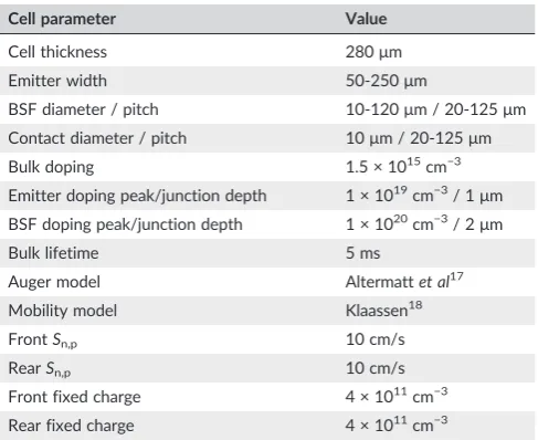
profile for the emitter and BSF is defined by a Gaussian decay with a set peak dopant concentration and junction depth. The width of the half unit cell is 500μm. The number of localized diffusions is based on the remaining area after the width of the emitter, and radius of the localized diffusion is taken into account. The parameters for the cell are shown in Table 1.
A 3‐dimensional schematic of the unit cell of the IBC model defined in TCAD is presented in Figure 2A. We first optimized the width of the emitter (Ew) and BSF (Bw) regions, and therefore the
[image:3.595.54.372.50.169.2]emit-ter fraction. Figure 2B plots the efficiency as the widths of the doped regions are varied between 50 and 250μm (overlaid, numbered diago-nal lines indicate the emitter fraction). In the case of the BSF, the width refers to the area in which localised diffusions were used (see Figure 1).
FIGURE 1 Schematic (top view) of the interdigitation in an interdigitated back contact cell, with boron‐doped emitter fingers (in yellow), localised phosphorus‐doped back surface field (BSF; in blue), and localised contact holes (in grey). The dimensions optimized using the TCAD model are labelled and include width of thep+emitter (E
w) and n+
BSF (Bw) regions; the contact finger widths for
n+region (nCF) andp+region (pCF); the
diameter of the local diffusion hole size for the BSF (locDF) and contact hole (Cw), as well as
pitch (Cg) for both. [Colour figure can be
viewed at wileyonlinelibrary.com]
TABLE 1 Input parameters for Sentaurus TCAD model sweep
Cell parameter Value
Cell thickness 280μm Emitter width 50‐250μm
BSF diameter / pitch 10‐120μm / 20‐125μm Contact diameter / pitch 10μm / 20‐125μm Bulk doping 1.5 × 1015cm−3
Emitter doping peak/junction depth 1 × 1019cm−3/ 1μm
BSF doping peak/junction depth 1 × 1020cm−3/ 2μm Bulk lifetime 5 ms
Auger model Altermattet al17
Mobility model Klaassen18
FrontSn,p 10 cm/s
RearSn,p 10 cm/s
[image:3.595.307.551.558.757.2]The contact finger widths (nCF and pCF) were kept the same as the doped region widths, with contact lumped series resistance (Rs)
calcu-lated usingGrid15for the varying contact fraction. These results reveal
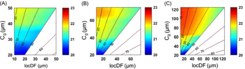
3 local efficiency optima at emitter/BSF ratios of 75:75, 75:50, and 125:125, as indicated by the overlaid triangles in Figure 2B. These values for the emitter and BSF were then used to find an optimum local diffusion hole size of the BSF (locDF) and an optimum contact pitch (Cg).
The results of this are illustrated in Figure 3, where efficiency contours are plotted and different ratios of hole size to pitch are overlaid as diagonal lines. Data for ratios above 50% were omitted as the BSFs overlap and are no longer locally diffused. Increasing the pitch whilst reducing the contact hole size is seen to increase efficiency, predominantly due to improvement in Voc. The optimum cell
performance is found for the 125:125 emitter:BSF width ratio, with a pitch size of 100μm and hole size of 30μm.
As a validation of the model and comparison to state‐of‐the‐art for diffused junction cells from literature, the optimized geometrical parameters (Geo‐A) established in this work were compared against that of the IBC work reported in Franklinet al4(Geo
‐B), using both Sentaurus TCAD and Quokka. For consistency, the remaining parame-ters were taken from the IBC cell reported in Fellet al.16The results
are shown in Table 2. The high efficiency potential of the optimized geometry is observed, with a modest gain inVoccompared to the work
in Franklinet al.4Thus, the fabrication process in this work is based on the TCAD‐optimized interdigitation design (GeoA) with Ew= 125μm,
Bw= 125μm, locDF = 30μm, Cg= 100μm, nCF = 125 μm, and
pCF = 125μm.
3
|E X P E R I M E N T A L M E T H O D S
3.1
|Device fabrication
[image:4.595.84.513.50.198.2]The device fabrication process is illustrated in Figure 4 and was based on a recipe taken from Franklinet al,4with the modified interdigitation design from the TCAD study above. Starting substrates weren‐type FZ wafers (4″, <100>, 1‐5Ω‐cm, 280μm, double‐side polished). In all cases, these were initially cleaned using RCA1, RCA2, and a dilute Hydrofluoric (HF) acid solution. Wafers undergoing the bulk FZ treat-ment were subjected to a double‐sided dry oxidation for 30 minutes at 1050°C (1), which was subsequently stripped in HF (2). Processing for treated and control wafers was therein identical. A 230 nm
FIGURE 2 A) Schematic of a unit cell used to simulate the interdigitated back contact cell in the 3D technology computer aided design model; B) solar cell efficiency (%) for varying widths of emitter and back surface field regions. The triangles indicate the efficiency optima. [Colour figure can be viewed at wileyonlinelibrary.com]
FIGURE 3 Plots of cell efficiency (%) as a function of diameter of localised diffusion (locDF) and pitch (Cg) for the optimum emitter:BSF ratios of A)
[image:4.595.307.550.286.356.2]75:75; B) 75:50; and C) 125:125, identified by the overlaid triangles in Figure 2B. [Colour figure can be viewed at wileyonlinelibrary.com]
TABLE 2 Performance of cell under Geo‐A and Geo‐B modelled in TCAD and Quokka
Jsc(mA/cm−2) Voc(mV) FF (%) η(%)
Geo‐A (TCAD) 42.0 709 83.6 24.9 Geo‐B (TCAD) 42.0 705 83.3 24.7 Geo‐A (Quokka) 41.6 703 83.9 24.5 Geo‐B (Quokka) 41.6 700 83.8 24.4
[image:4.595.98.501.615.729.2]double‐sided wet thermal oxide was grown at 1000°C for 45 minutes in a Tempress (TS8603) tube furnace to act as then+(local BSF)
diffu-sion mask (3). Holes for the local BSF were opened in the oxide layer via photolithography and etching, either with a dry, reactive ion etch or a wet etch (4). The positive lithography process for the BSF mask used AZ6632 resist that was spun at 4000 rpm, soft baked for 1 minute at 110°C on a hotplate, exposed with a broadband UV source at a total fluence of 130 mJ/cm2, developed in AZ826 for 30 s, and finally hard
baked at 145°C for 10 minutes on a hotplate. For the dry‐etched cells, the subsequent etch step used a plasma process with a CF4/O2
ambi-ent (OPT Plasmalab System 100, 35/3 sccm, 165 W, 380 V DC bias, 6 minutes). For the wet‐etched cells, a buffered HF (7:1) etch was instead used to transfer the pattern from the resist to the oxide, with an etch time of 270 s at 25°C. As will be shown below, the dry‐etch process was abandoned in favour of wet etching due to severe degra-dation of the bulk lifetime following diffusion. The resist was then removed using acetone and DI water.
Phosphorous doping for the local BSF was undertaken via POCl3
diffusion in a tube furnace (5). This consisted of a pre‐diffusion depo-sition step at 795°C for 25 minutes with a 1:1 POCl3:O2gas ratio,
followed by a 1‐hour drive‐in at 920°C. The phosphosilicate glass andn+diffusion mask were removed with dilute HF. The creation of
thep+emitter regions involved growth of a double‐sided wet thermal oxide diffusion mask (6), and photolithographic patterning and etching to define the mask openings (7). Parameters for these steps were iden-tical to those described above for the BSF regions. Boron doping was undertaken via tube diffusion using a liquid BBr3 source (8). This
consisted of a deposition step at 850°C with a 1:1 O2:BBr3gas ratio,
followed by a drive‐in at 920°C and an in situ oxidation to dissolve any potential potential boron‐rich layer (BRL) of SiB6formed during
the process. The borosilicate glass andp+diffusion mask were then removed using dilute HF.
With thep+andn+regions defined on the rear surface, both the front and rear surfaces were passivated (9). First, the rear surface was passivated with a 10‐nm layer of Al2O3deposited by atomic layer
deposition (ALD; 110 cycles at 200°C, Cambridge Savannah) and capped with a 60‐nm layer of PECVD SiNx:H (Roth and Rau, AK400).
The wafer was then dipped in dilute HF to remove the unavoidable Al2O3deposition around the edges of the front surface, before
[image:5.595.70.358.51.481.2]passiv-ating the front surface with a single 80‐nm layer of PECVD SiNx:H. To FIGURE 4 Process flow of fabricating the interdigitated back contact cell, with numbers corresponding to the description in Section 3. [Colour figure can be viewed at
activate the Al2O3passivation, the wafer was subsequently annealed
in an RTA at 400°C for 10 minutes in a N2ambient. The final step of
metallization was achieved using 2 lithography steps. In the first step, 10‐μm diameter contact holes were opened in the rear passivation stack using the same positive process as for then+diffusion mask,
but with the wet etch time increased to 10 minutes to fully clear the Al2O3/SiNxstack (10). A second lithography step, based on a negative
resist lift‐off process, was then used to define the contact fingers (11). This consisted of a dehydration bake (180°C, 5 minutes), resist spin-ning (AZ nLOF2035, 3000 rpm for 30 s), hotplate soft bake (1 minute, 110°C), exposure (i‐line, 72 mJ/cm2), development (AZ826, 60 s), and
finally a hotplate hard bake (150°C, 5 minutes). With the contact finger mask in place, the wafer was given a brief dip in 7:1 buffered HF for 3 s to remove any native oxide immediately before deposition of a 1μm thick aluminium layer via e‐beam evaporation or thermal evaporation. Metal lift‐off was achieved by soaking in acetone and ultrasonic agita-tion (12). The final step was a 1‐minute sinter at 350°C in an N2
ambi-ent to help lower the contact resistance and form an ohmic contact.
3.2
|Characterization
The devices were characterized using several techniques. Doping pro-files of thep+andn+regions were measured using an electrochemical
capacitance voltage tool (WEP, CVP21). The passivation quality and effective minority carrier lifetime were measured quantitatively using transient or quasi‐steady‐state PC on a Sinton WCT‐120 lifetime tes-ter with an inductive coil modified to measure small (2 × 2 cm) samples and qualitatively using PL imaging (BTi LIS‐R1) at various stages during
fabrication, on the cells themselves and on test wafers. The accuracy of all PL images was improved by applying point spread function deconvolution.19Al
2O3deposited by ALD was used as a passivation
layer to investigate RIE damage. Photoconductance measurements were also performed on some finished cells that were stripped back (HF and alkaline etch) to the bare wafer and re‐passivated to investi-gate bulk lifetimes. All stated carrier lifetimes were extracted from PC measurements at an excess carrier density of 1015cm−3.I‐V charac-teristics of cells were measured without temperature control using a triple A class solar simulator (ABET Technologies Sun 3000) with a source measurement unit.
4
|R E S U L T S
4.1
|Damage from electron beam evaporation of
metal contacts
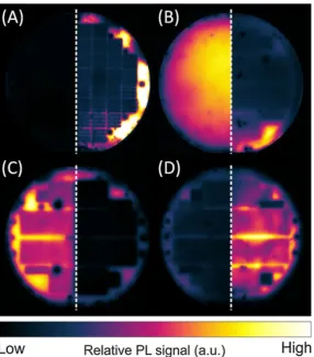
Lifetime degradation was clearly observed in our wafers via PL images taken before and immediately after electron beam evaporation of the metal contacts, including in non‐metallized regions. The left half of Figure 5A shows the PL image of a wafer after e‐beam evaporation, while the right half shows the same wafer after sintering (350°C, 1 min-ute, N2). The imaging conditions (1 s exposure, 1 sun illumination) and
[image:6.595.242.529.430.756.2]colour scales are identical for both. The lack of PL signal in the left‐ hand image indicates the heavy presence of defects that promote nonradiative recombination, despite a passivation anneal at 420°C prior to metallization. We suggest that this is likely due to X‐rays
FIGURE 5 A) Photoluminescence (PL) image of wafer pre‐sintering (left) and post‐sintering (right); B) PL image of wafer pre‐RIE (left) and post‐RIE (right) etch; C) PL image of wafer using buffered HF etch (left) and RIE etch (right) with proceeding boron diffusion; D) PL image of wafer without (left, cell A) and with (right, cell B) bulk float‐zone treatment. All wafers are 4″in diameter. All images are at 1 sun, with exposure times of 1 s for (A) and 0.1 second for (B), (C), and (D). The relative PL signal is only directly comparable between the 2 samples (left and right) in each frame (A‐D). [Colour figure can be viewed at
wileyonlinelibrary.com]
emitted during electron‐beam evaporation of the aluminium, which are known to cause material degradation in the form of increased oxide traps, charges, and surface states.20-22A dramatic increase in the PL
counts (relative increase in lifetime and Voc) is seen following the
sintering step (right‐hand image), particularly for the undiffused and non‐metallized region around the perimeter. The sintering treatment appears to reverse some of the damage during electron beam evapora-tion. Further improvements are expected by replacing electron‐beam evaporation with a thermal evaporation process, which would avoid the generation of damaging X‐rays during metallization.
4.2
|RIE damage
When dry etching was used for pattern transfer prior to diffusion (steps 4 and 7 in Figure 4), low PL counts were observed in patterned regions of the wafer (Figure 5B, right side), whereas lifetime monitor wafers maintained high PL counts (Figure 5B, left side). These monitors underwent identical diffusion and passivation steps, but did not undergo any patterning. RIE‐induced damage of the patterned area was therefore suspected. Shallow implantation of reactive ions as well as lattice damage has been shown to produce surface degradation in silicon.23-27The right‐hand image in Figure 5C shows a PL image of a test wafer patterned using RIE, then doped using BBr3diffusion and
finally passivated with ALD Al2O3. The patterned areas appear black,
indicating that the RIE‐induced degradation is dramatically enhanced after subsequent dopant diffusion due to drive‐in of the implanted ions deeper into the bulk and the formation of recombination active defects. The process was repeated but with a buffered HF etch used instead of RIE. The PL image of the resulting sample (Figure 5C, left side) illustrates that significant improvements in lifetime are achieved with wet etching compared to the dry etching process. This is sup-ported by PC measurements (Figure 6), which reveal an increase in effective minority carrier lifetime in cells, after passivation anneal and before contact opening (ie, after step 9 in Figure 4), from <100 to 460μs when RIE was replaced by wet etching for the pre‐diffusion pattern transfer steps. The measurements in Figure 6 are aggregated
transient measurements, as multiple cells are measured over the sen-sor region, including the higher lifetime regions in between the cells. Therefore, the lifetime measurements in Figure 6 could be overestimated, and thus the actual bulk lifetime of the cells is likely to be slightly lower than measured.
4.3
|Bulk defects
Recent literature has shown the presence of grown‐in defects limiting the lifetime of commercially manufactured FZ silicon.6,7,28Although initially often latent, such defects can become recombination‐active and hence reduce bulk lifetime after heat treatments at moderate tem-peratures (450‐750°C). Fortunately, this effect can be removed by annihilating the defects with a high‐temperature oxidation (>1000°C) and subsequent oxide strip, thereby stabilizing the bulk lifetime against future thermal treatments. To explore the influence of this bulk FZ treatment on the IBC cell performance, 2 wafers were put through the cell fabrication process in Figure 4; one as‐grown (cell A) and a sec-ond with the bulk FZ treatment (cell B) of a dry oxidation (1050°C/30 mins) and wet chemical strip. All other processing was identical. Figure 5D shows a PL image of wafers (processed up to step 9 in Figure 4), without (left, cell A) and with (right, cell B) the bulk FZ treat-ment. The significantly higher PL counts for the treated wafer clearly illustrate the benefit of the bulk FZ treatment on the carrier lifetime. This is supported by PC lifetime measurements that indicate an increase in minority carrier lifetime from 460μs to 1.8 ms when using wafers subjected to the bulk FZ treatment (Figure 6). This translates to improvement at the final cell level, as shown by theI‐Vcharacteristics of cells with and without the bulk FZ treatment presented in Figure 7. From this, we can see a 28% relative increase in efficiency (from 14.3% to 18.3% absolute) due to the boost in lifetime conferred by the bulk FZ treatment.
Further investigation of the improvements to bulk lifetime was undertaken. Effective lifetime (τeff) measurements of the base material
[image:7.595.65.269.529.696.2](3.2Ω‐cmn‐type) from 2 IBC cells (without (cell A) and with (cell B) the bulk FZ treatment) were analysed, following dielectric removal and a diffusion etch using HF and 25% TMAH, respectively. The 2 × 2 cm cell
FIGURE 6 Measured effective minority carrier lifetime of cells on float‐zone (FZ) 3.2Ω‐cmn‐type silicon wafer (prior to metallisation) for RIE‐etched cells, wet‐etched cells (cell A) and wet‐etched cells with bulk FZ treatment (cell B). [Colour figure can be viewed at
wileyonlinelibrary.com]
[image:7.595.326.531.550.717.2]samples were passivated by dipping them in a superacid (SA) solution of trifluoromethanesulfonimide dissolved in dichloroethane (2 mg/ mL) as outlined in Bullocket al29and Grantet al.30In this case, the
pas-sivation is assumed to be conformal (i.e. it also passivates the edges). The SA passivation process occurs at room temperature, so artefacts that occur because of annealing during passivation by conventional dielectrics are avoided.
To investigate/remove edge recombination effects on the 2 × 2 cm IBC cell samples, 2 additional control 270μm thick FZ 2.6
Ω‐cm n‐type samples were passivated with SA, (1) a 4‐inch quarter sample and (2) a 2 × 2 cm sample from the same wafer. From the resulting lifetime results presented in Figure 8, it is evident that SA passivation provides excellent surface passivation, yielding a τeffof
approximately 5 ms on the larger quarter wafer sample (blue circles). In contrast, the smaller 2 × 2 cm control sample yields aτeffof
approx-imately 4 ms (orange squares), which we attribute to edge recombina-tion effects that do not impact the larger sample. In both cases, however, the surface recombination velocity of SA‐passivated silicon is predicted to be 0.65 ± 0.05 cm/s using theSparameterisation devel-oped in Grantet al.30Therefore, to correct for a surface recombination velocity, S, of 0.65 ± 0.05 cm/s (front/back) on both control samples, we have used the following equation31(whereWcorresponds to the sample thickness):
1=τeff¼1=τbulkþ2S=W; (1)
whereby the dashed blue line in Figure 8 represents the calculated bulk minority carrier lifetime (τbulk) and the dashed brown line represents
the edge affectedτeffof the smaller 2 × 2 cm control sample.
There-fore, the difference between the true bulk lifetime (blue dashed line) and edge affected lifetime of the smaller 2 × 2 cm sample (brown dashed line) yields a total “effective” edge recombination velocity (Sedge) of approximately 0.7 cm/s.
Turning back to the 2 IBC cell samples, Figure 9A plots the measured effective lifetime of cell A (no bulk FZ treatment) and cell B (with bulk FZ treatment) after removal of the dielectric layer and diffused region and subsequent passivation with SA. Before correcting for both surface and edge recombination, it is evident that cell A has a lower bulk lifetime compared to cell B. However, to ascertain the true bulk lifetime of each cell material, both surface (S= 0.55 ± 0.05 cm/s) and edge recombination (Sedge= 0.7 cm/s) effects were removed from
the measuredτeff. In this case, a lowerSvalue is used because the
dop-ing of the cell material is lower compared to the control samples of Figure 8, thereby resulting in a slightly lowerSas outlined in Grant
et al.30The true bulk lifetime of each cell is therefore given by the dashed lines in Figure 9A. As seen in Figure 9A, the actual difference in bulk lifetime is approximately 2 ms once external recombination mechanisms are accounted for (surface and edge).
[image:8.595.64.270.494.665.2]Finally, to quantify the bulk lifetime reduction during IBC cell fabrication, Figure 9B plots the effective (solid symbols) and bulk lifetimes (dashed lines) of 2 silicon wafers (neither of which were subjected to the bulk FZ treatment), (1) in the as‐received condition and (2) after the boron diffusion, which was subsequently etched away prior to SA passivation. From Figure 9B, it is evident that the “as‐ received”silicon wafer yields a very highτbulkof >20 ms (τeff> 10 ms), thereby indicating the material of choice is suitable for IBC cells. How-ever, when a sister silicon wafer underwent a boron diffusion, as outlined in section 3.1, a significant reduction in the bulk lifetime was observed, whereτbulkvalues of <2 ms were measured. Although the boron‐diffused wafer shows a lowerτbulkthan the cell wafers shown in
Figure 9A, we postulate that theτbulkof the cell wafers has been pre-served by the heavy phosphorus diffusion, in which case some gettering has occurred as previously demonstrated in Zhenget al.33 Although we do not understand the cause for the large reduction in
τbulkfollowing the boron diffusion, we can postulate that some level of contamination has occurred during this process, which could be reduced by removing the BRL by a wet chemical process to prevent any impurities in the BRL being diffused into the bulk material during the traditional in situ oxidation to dissolve the BRL.18On the contrary, it is also known that boron diffusions can form dislocations that diffuse into the bulk material, which have shown dependence on the BRL thickness.34Therefore, to minimise bulk degradation during cell
fabri-cation, an optimised boron diffusion process, which limits bulk contam-ination or defect formation, is required and/or a phosphorus diffusion barrier is necessary to minimise any contamination or defect penetra-tion resulting from the boron diffusion (ie, front side n+protection
layer). In the latter case, the protectiven+layer can be removed during front‐side texturing or immediately before surface passivation.
4.4
|Further analysis with TCAD modelling
To observe the influence of varying lifetime on the IBC cell, we used the TCAD model but replaced the doping profile for the emitter and BSF with ECV measured experimental data, as well as typical fixed charge, interface defect density, and capture cross‐sectional data for the dielectric/doped (n,n+, andp+) interfaces used for the solar cells.
The bulk lifetime was then varied to gauge its influence on efficiency. The same sweep was undertaken when the lumped resistance (calculated
FIGURE 8 Effective/bulk lifetime of FZ 2.6 Ω‐cm n‐type silicon superacid‐passivated control samples. Blue circles,τeffmeasurement
on a quarter sample; blue dashed line, bulk lifetime after correcting for
S= 0.65 ± 0.05 cm/s; orange squares,τeffmeasurement of a 2 × 2 cm
sample from the same wafer; brown dashed line, 2 × 2 cmScorrected lifetime, but without edge recombination correction. The black line corresponds to the intrinsic limit.32[Colour figure can be viewed at wileyonlinelibrary.com]
usingGrid15) from the cell was reduced by increasing the thickness of the
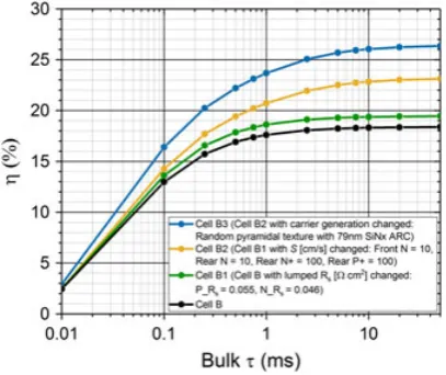
metal contacts to 4μm (a key limiting factor in the latest cell fabrication batch is that metal contacts were only 1μm in thickness). Furthermore, to observe the influence of lifetime under improved passivation, the sweep was undertaken with S values reduced to 10 cm/s on undiffused and 100 cm/s for diffused interfaces. Finally, the solar cell efficiency as a function of the bulk minority carrier lifetime is shown when light trapping with ARC is used to increase the carrier genera-tion rate, Gopt.
The results are illustrated in Figure 10. This shows that the effi-ciency significantly increases for lifetime values up to 2 ms and remains roughly constant for higher lifetime values. The same is the case for increased lumpedRs. However, with improvedS(and enhanced carrier
generation), the plateau is shifted to lifetime values exceeding 10 ms. The modelled results show that for cell B, a difference inτbulkof 2 to
5 ms does not result in any significant change of efficiency perfor-mance, unlike our experimental data, which showed a 28% increase.
The lifetime measurements of the cell wafers shown in Figure 6 (cells A and B), however, are significantly lower. We therefore postulate that the significant difference in lifetime between cell A with Al2O3/SiNx
passivation (Figure 6) and cell A with SA passivation (Figure 9A) is not limited by surface recombination but rather bulk, which can only occur if the defect present in cell A (passivated with Al2O3/SiNx) is
partly removed during the TMAH etch (approximately 5μm per side) to remove the diffused regions prior to SA passivation. This indicates that some portion of the grown‐in defect diffuses towards the surface during the various thermal processes, suggesting that this approach is still not as effective as performing a single high‐temperature thermal oxidation prior to IBC fabrication, where the grown‐in defect can out‐diffuse more efficiently. Our results indicate that vacancies could be the diffusing species, as suggested by Voronkov and Falster8; how-ever, the exact nature of the defect and how it diffuses/changes with thermal treatments is still unclear. Nevertheless, our measurements indicate that the bulk lifetime measurements for cell A were overesti-mates following SA passivation due to the etch‐back required to remove the diffused regions of the cell, and thus any bulk defects within approximately 5μm of the surfaces. It should be noted that the lower lifetimes shown in Figure 6 are also overestimates due to being aggregated transient measurements on whole wafers (not only cell areas; see Section 4). The efficiency improvement observed in the TCAD simulations also highlights the potential for this IBC cell when very high bulk lifetime values can be maintained (approximately 10 ms), withη> 19% for improvedRs,η> 22% for improvedSand
η> 26% with improved light trapping. It should be noted that the model does not take into account edge recombination.
5
|C O N C L U S I O N
[image:9.595.125.473.51.206.2]Interdigitated back contact cells were fabricated with and without a bulk FZ treatment, with the former showing a 28% relative increase in efficiency (from 14.3% to 18.3% absolute). Minority carrier lifetime analysis of the wafers showed a significant increase in the maximum effective lifetime from 460μs to 1.8 ms due to the bulk FZ treatment.
FIGURE 9 Superacid (SA)‐passivated effective/bulk lifetime of FZ 3.2Ω‐cmn‐type silicon. A)τeffmeasurement of 2 × 2 cm cell A (no bulk float‐ zone [FZ] treatment, red squares) and cell B (bulk FZ treatment, green circles). The figure also plotsτbulkfor cell A (red dashed line) and cell B (green
dashed line) after correcting for bothSandSedge. B)τeff(solid symbols) andτbulk(dashed lines) of two silicon wafers, (i) in the as‐received condition
and (ii) after a boron diffusion, which was subsequently etched away prior to SA passivation. The black lines represent the intrinsic limit.32[Colour
figure can be viewed at wileyonlinelibrary.com]
FIGURE 10 Modelled 1‐sun solar cell efficiency as a function of the bulk minority carrier lifetime. The solar cell was simulated in
[image:9.595.66.270.515.686.2]Furthermore, once the cells were stripped of their diffused areas and re‐passivated using SA, bulk lifetime values of 2 ms (cell A) and 5 ms (cell B) were found for wafers without and with the bulk FZ treatment, respectively, suggesting a near surface defect was present in the cell wafers that affected the untreated wafer more severely compared to the treated wafer. TCAD simulations predict that this difference in bulk lifetime would not result in a significant efficiency improvement. How-ever, upon careful examination of the bulk lifetime of cell A before and after etching the diffused regions, it is suggested that bulk defects were present in the near surface region, thus limiting the bulk lifetime to <460μs on the cell level. This lifetime was boosted to approxi-mately 2 ms once approxiapproxi-mately 5 μm of silicon was removed from the surface prior to SA passivation. In this case, the lifetime increase from <460μs (cell A) to 5 ms (cell B) is consistent with the enhance-ment in efficiency as simulated by TCAD and our experienhance-mental data. TCAD simulations showed that this bulk lifetime boost can result in significant enhancement of performance in the cells when maintaining low‐surface recombination velocities. Furthermore, the simulations also highlighted the potential for high performance of these cells through improved series resistance, passivated regions, and light trap-ping, withη> 26% forτ> 10 ms. Other degradation mechanisms in the fabrication process, which limited performance, were observed in this work, including e‐beam evaporation and RIE damage. Photoluminescence studies showed improvements when metallization was followed by a sinter and when dry etching during the pre‐diffusion pattern transfer was replaced with wet etching.
A C K N O W L E D G E M E N T S
T. Rahman and S.A. Boden acknowledge support from the Supersolar Solar Energy Hub (EPSRC grants EP/J017361/1 and EP/M014797/1). A. To acknowledges the Australian Renewable Energy Agency for his PhD scholarship. N.E. Grant and J.D. Murphy acknowledge funding from the EPSRC SuperSilicon PV project (EP/M024911/1). This work was performed in part at the NSW Node of the Australian National Fab-rication Facility. All data supporting this study are openly available from the University of Southampton repository at http://doi.org/10.5258/ SOTON/D0188
O R C I D
Tasmiat Rahman http://orcid.org/0000-0002-6485-2128
John D. Murphy http://orcid.org/0000-0003-0993-5972
Stuart A. Boden http://orcid.org/0000-0002-4232-1828
R E F E R E N C E S
1. Yoshikawa K, Kawasaki H, Yoshida W,et al. Silicon heterojunction solar cell with interdigitated back contacts for a photoconversion efficiency over 26%.Nat Energy. 2017;2:17032.
2. Rahman T, Bonilla RS, Nawabjan A, Wilshaw PR, Boden SA. Passivation of all‐angle black surfaces for silicon solar cells. Sol Energy Mater Sol Cells. 2017;160:444‐453.
3. Savin H, Repo P, von Gastrow G,et al. Black silicon solar cells with interdigitated back‐contacts achieve 22.1% efficiency. Nat Nanotechnol. 2015;10(7):624‐628.
4. Franklin E, Fong K, McIntosh K,et al. Design, fabrication and character-isation of a 24.4% efficient interdigitated back contact solar cell.Prog Photovolt. 2016;24(4):411‐427.
5. Trupke T, Bardos RA, Hudert F, Würfel P, Zhao J, Wang A, Green MA. Effective excess carrier lifetimes exceeding 100 milliseconds in float zone silicon determined from photoluminescence. In Proceedings of the 19th European Photovoltaic Solar Energy Conference, Paris, France. 2004:758‐761.
6. Grant NE, Markevich VP, Mullins J,et al. Permanent annihilation of thermally activated defects which limit the lifetime of float‐zone silicon.
Phys Status Solidi A. 2016;213(11):2844‐2849.
7. Grant NE, Markevich VP, Mullins J, Peaker AR, Rougieux F, Macdonald D. Thermal activation and deactivation of grown‐in defects limiting the lifetime of float‐zone silicon.Phys Status Solidi RRL. 2016;10(6):443‐447. 8. Voronkov V, Falster R. Vacancy out‐diffusion in nitrogen‐doped silicon.
Phys Status Solidi C. 2012;9(10–11):1987‐1991.
9. Abe T, Takahashi T. Intrinsic point defect behavior in silicon crystals during growth from the melt: a model derived from experimental results.J Cryst Growth. 2011;334(1):16‐36.
10. Murphy JD, Al‐Amin M, Bothe K, Olmo M, Voronkov V, Falster R. The effect of oxide precipitates on minority carrier lifetime in n‐type silicon.
J Appl Phys. 2015;118(21):215706
11. Søndenå R, Hu Y, Juel M, Wiig MS, Angelskår H. Characterization of the OSF‐band structure in n‐type Cz‐Si using photoluminescence‐ imaging and visual inspection.J Cryst Growth. 2013;367:68‐72. 12. Haunschild J, Reis IE, Geilker J, Rein S. Detecting efficiency‐limiting
defects in Czochralski‐grown silicon wafers in solar cell production using photoluminescence imaging.Phys Status Solidi RRL. 2011;5(5–6):199‐201.
13. Synopsys.Sentaurus TCAD Version K‐2015.06. Mountain View, CA: Synopsys Inc.; 2015.
14. https://www2.pvlighthouse.com.au/calculators/opal%202/opal%202. aspx.
15. https://www2.pvlighthouse.com.au/calculators/Grid%20calculator/ Grid%20calculator.aspx.
16. Fell A, McIntosh KR, Altermatt PP,et al. Input parameters for the sim-ulation of silicon solar cells in 2014.IEEE J Photovolt. 2015;5(4):1250‐ 1263.
17. Altermatt PP, Schmidt J, Heiser G, Aberle AG. Assessment and parameterisation of Coulomb‐enhanced Auger recombination coeffi-cients in lowly injected crystalline silicon. J Appl Phys. 1997;82(10):4938‐4944.
18. Klaassen D. A unified mobility model for device simulation—I. Model equations and concentration dependence. Solid‐State Electron. 1992;35(7):953‐959.
19. Payne DNR, Vargas C, Hameiri Z, Wenham SR, Bagnall DM. An advanced software suite for the processing and analysis of silicon lumi-nescence images.Comput Phys Commun. 2017;215:223‐234. 20. Ning TH. Electron trapping in SiO2 due to electron‐beam deposition of
aluminum.J Appl Phys. 1978;49(7):4077‐4082.
21. Collins D, Sah C. Effects of X‐ray irradiation on the characteristics of metal‐oxide‐silicon structures.Appl Phys Lett. 1966;8(5):124‐126. 22. Hamasaki M. Radiation effects on thin‐oxide MOS capacitors caused
by electron beam evaporation of aluminum. Solid‐State Electron. 1983;26(4):299‐303.
23. Jansen H, Gardeniers H, de Boer M, Elwenspoek M, Fluitman J. A sur-vey on the reactive ion etching of silicon in microtechnology. J Micromech Microeng. 1996;6(1):14.
24. Oehrlein GS, Tromp R, Tsang J, Lee Y, Petrillo E. Near‐surface damage and contamination after CF 4/H 2 reactive ion etching of Si. J Electrochem Soc. 1985;132(6):1441‐1447.
25. Connick IWH, Bhattacharyya A, Ritz KN, Smith WL. Study of reactive‐ ion‐etch‐induced lattice damage in silicon by Ar, CF4, NF3, and CHF3
plasmas.J Appl Phys. 1988;64(4):2059‐2063.
26. Pang S, Rathman D, Silversmith D, Mountain R, DeGraff P. Damage induced in Si by ion milling or reactive ion etching. J Appl Phys. 1983;54(6):3272‐3277.
27. Ikawa E, Endo N, Tajima M, Kurogi Y. Annealing and oxidation effects after CF4/H2 dry etching for damage recovery. Surf Sci.
1986;172(3):763‐772.
28. Rougieux FE, Grant NE, Barugkin C, Macdonald D, Murphy JD. Influ-ence of annealing and bulk hydrogenation on lifetime‐limiting defects in nitrogen‐doped floating zone silicon. IEEE J Photovolt. 2015;5(2):495‐498.
29. Bullock J, Kiriya D, Grant N,et al. Superacid passivation of crystalline silicon surfaces.ACS Appl Mater Interfaces. 2016;8(36):24205‐24211. 30. Grant NE, Niewelt T, Wilson NR,et al. Superacid‐Treated Silicon
Sur-faces: Extending the Limit of Carrier Lifetime for Photovoltaic Applications.IEEE J Photovolt. Under Review2017.
31. Sproul A. Dimensionless solution of the equation describing the effect of surface recombination on carrier decay in semiconductors.J Appl Phys. 1994;76(5):2851‐2854.
32. Richter A, Glunz SW, Werner F, Schmidt J, Cuevas A. Improved quanti-tative description of Auger recombination in crystalline silicon.Phys Rev B. 2012;86(16):165202.
33. Zheng P, Rougieux F, Samundsett C,et al. Upgraded metallurgical‐ grade silicon solar cells with efficiency above 20%. Appl Phys Lett. 2016;108(12):122103.
34. Kessler MA, Ohrdes T, Wolpensinger B, Harder N‐P. Charge carrier life-time degradation in Cz silicon through the formation of a boron‐rich layer during BBr3 diffusion processes. Semicond Sci Technol.
2010;25(5):055001.
![FIGURE 4Process flow of fabricating theinterdigitated back contact cell, with numberscorresponding to the description in Section 3.[Colour figure can be viewed atwileyonlinelibrary.com]](https://thumb-us.123doks.com/thumbv2/123dok_us/9431641.448985/5.595.70.358.51.481/figure-process-fabricating-theinterdigitated-numberscorresponding-description-section-atwileyonlinelibrary.webp)