OF HVDC CONVERTORS
A thesis
presented for the degree of
Doctor of Philosophy in Electrical Engineering in the
University of Canterbury Christchurch
New Zealand
by
J.e.
Graham B.E. (Hons)TABLE OF CONTENTS
List of Figures
List of Symbols and Abbreviations
Abstract
Acknowledgements
Chapter 1
Chapter 2
Introduction
System Hardware 2.1 Introduction 2.2 Convertor Model
2.3 Microprocessor System 2.3.1 Introduction
2.4
2.3.2 Choice of Microprocessor
2.3.3
2.3.4 2.3.5
2.3.2.1 Single or Multiple Processor 2.3.2.2 Processor Size
2.3.2.3 Departmental Support 2.3.2.4 Board Level Products 2.3.2.5 Bus Structure
2.3.2.6 Local Boards 2.3.2.7 Commercial Boards 2.3.2.8 Newer Processors Support Boards
Chapter 3
Chapter 4
Chapter 5
System Software
3.1 Operating System
3.1.1 Choice of Operating System
3.1.2 RMX 86 Operating System 3.1.3 Operating System Overheads
3.2 Languages
3.2.1 Choice of Languages
3.2.2 Feature of PLM 86
3.3 Software Development Techniques
Data Acquisition Sub-System
4.1 Sub-system Requirements
4.1.1 Control Sub-System
4.1.2 Fault Simulation and Detection Sub-Systems
4.1.3 Interactive Analysis Sub-System
4.2 Convention and Storage Modes
4.3 Convertor Angle Measurement
4.3.1 On/Off and Zero Crossing Detection
4.3.2 Data Acquisition Interrupts
4.3.3 Angle Calculation
4.4 Direct Current Measurement
4.5 Resolution and Accuracy
4.5.1 Angle Measurements
4.5.2 DC Current
Control Sub-System
5.1 HVDC Control
5.1.1 Basic Control Principles
5.2 Analogue Implementations
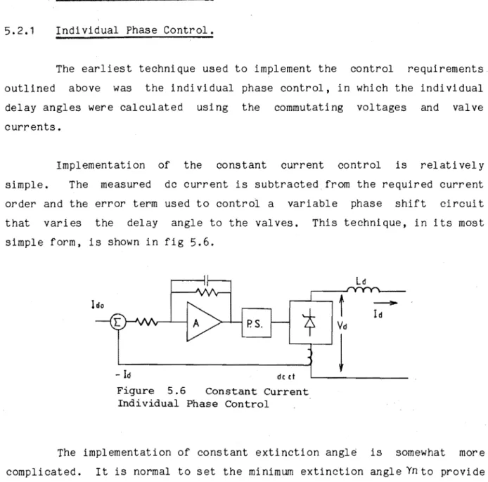
5.2.1 Individual Phase Control
5.2.2 Equidistant Control
5.3 Direct Digital Control
5.3.1 Discrete Logic Based Schemes
5.3.2 Micro/Mini Computer Based Schemes
5.4 Microprocessor Based Control Systems
5.4.1 Aims
5.4.2 Basic Control Algorithm
5.4.3 Microprocessor Implementation
Chapter 6
5.4.4 Interactive Capabilities
5.4.4.1 Operator Controllable Features 5.4.4.2 Convertor Information Display
Fault Simulation and Detection Sub-Systems 6.1 Convertor Faults
6.1.1 Commutation Failure 6.1.2 Fire Through
6.1.3 Misfire 6.2 Fault Simulation
6.2.1 Simulator Requirements 6.2.2 Existing Fault simulators
6.2.3 Microprocessor Based Fault Simulator 6.2.3.1 Basic Principles of Operation 6.2.3.2 Real Time Software
6.2.3.3 Interactive Software 6.3 Fault Detection
6.3.1 Existing Techniques
6.3.2 Direct Digital Fault Detection
6.3.3 Microprocessor Based Fault Detection 6.3.4.1 Theory of Operation
6.3.3.2 Implementation
6.3.3.3 Tracking Fault Developments 6.4 Fault Development Control
6.4.1 Princi pIes of Operation 6.4.2 Implementation
60 60 62 65 65 65 66 66 67 67 67 68 68 69 72 76 76 76 77 77 81 ·88 91 91 92
Chapter 7.0 Factors Affecting the Operation of Faul t Development Control 101
7.1 Effect of Short Circuit Ratio 101
7.1.1 Commutation Failures on Weak AC Systems 103 7.1. 2 Misfires on Weak AC Systems 107
7.2 Other Typical Convertor Faults 109
7.2.1 Double Successive Commutati on Failure 109
7.2.2 Rectifier Misfire 112
7.2.3 Single Phase AC Faults 11 4
8.0 Conclusions 123
References 125
Figure 1.1 2.1 2.2 2.3 2.lJ 2.5 2.6 2.7 2.8 2.9 2.10
lJ • 1
lJ.2 lJ.3 lJ.lJ lJ.5 lJ.6 lJ.7 lJ.8 lJ.9 5.1 5.2 5.3 5.lJ 5.5 5.6 5.7 5.8 5.9 5.10 5. 11
TABLE of FIGURES ,
HVDC Development System Block Diagram
Convertor Front Panel Mimic Convertor Firing Circuit
Prototype System Block Diagram System Memory Map
Development System Photograph
AID Board Block Diagram
Angle Measurement Board Block Diagram Buffer Stage Circuit Diagram
Zero Crossing Detector Circuit Diagram Zero Crossing Detector Waveforms
Data Acquisition Interrupt Routine Data Acquisition Mainline Routine Data Acquisition anI off Routine Data Acquisi tion Delcal Routine Data Acquisition Comcal Routine Data Acquisi tion Cross Routine Data Acquisition Extcal Routine
AID Timer Interrupt Routine
AID EOC Interrupt Routine
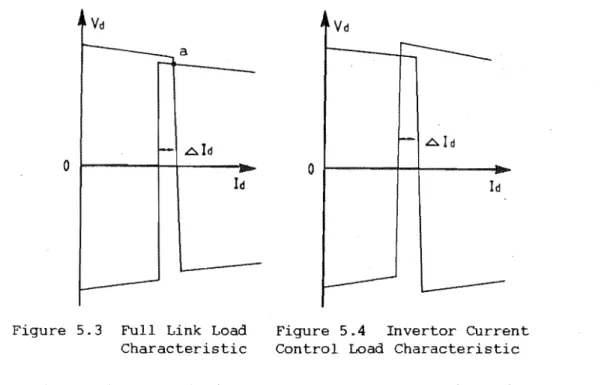
Basic Convertor Load Characteristic Basic Link Load Characteristic Full Link Load Characteristic
Invertor Constant Current Control Load Characteristic Link Equivalent Circuit
Constant Current Individual Phase Control Block Diagram
Page 2 5 6 9 16 17 19 21 20 22 23 36 38 39 lJO lJ1 lJ2 lJ3 lJlJ lJlJ lJ8 lJ8 lJ9 lJ9 50 51
Constant Extinction Angle Individual Phase Control Block Diagram 52
Equidistant Firing Control Block Diagram 53
Microprocessor Control Algorithm
Constant Extinction Angle Control Algorithm Microprocessor Control Timing Diagram
5.12 Operators Terminal Display 62
5.13 Controller step Response 63
6.1 Zero Crossing Interrupt Service Routine 70
6.2 Commutation Failure Timer Routine 72
6.3 Fire Through Timer Routine 72
6.4 Normal Invertor Operation Bargraph 74
6.5 Uncontrolled Misfire Bargraph 75
6.6 Uncontrolled Commutation Failure Bargraph 77
6.7 Uncontrolled Fire through Bargraph 78
6.8 Uncontrolled Misfire Bargraph 79
6.9 Fault Detection Interrupt Service Routine 81
6.10 Fault Detection Mainline Routine 81
6.11 Alternative Misfire Detection Routine 88
6.12 HVDC System Line Diagram 91
6.13 Controlled Commutation Failure Bargraph 93
6.14 Controlled Commutation Failure DC Voltage Waveform 94 6.15 Uncontrolled Commutation Failure DC Voltage Waveform 94
6.16 Controlled Fire Through Bargraph 94
6.17 Controlled Fire Through DC Voltage Waveform 95 6.18 Uncontrolled Fire Through DC Voltage Waveform 95 6.19 Uncontrolled Misfire DC Voltage Waveform 96
6.20 Controlled Misfire Bargraph 95
6.21 Controlled Misfire DC Voltage Waveform 96
6.22 Misfire Control Failure Bargraph 97
6.23 Misfire Control Failure DC Voltage Waveform 97 6.24 Controlled Misfire, Alternative Detection, DC Voltage Waveform 97 6.25 Controlled Misfire, Alternative Detection, Bargraph 98 6.26 Alternative Detection Timer Interrupt Routine 99 6.27 Controlled Misfire, Alternative Detection
Insufficient Delay, Bargraph 99
6.28 Controlled Misfire, Alternative Detection
Insufficient Delay, DC Voltage 100
7.1 HVDC System Line Diagram 101
7.2 Effect of SCR on Overlap 102
7.3 Unoontrolled Commutation Failure Bargraph 103
7.5
7.6
7.7
7.8
7.9
Filter Configuration
Uncontrolled Misfire Bargraph
Controlled Misfire, Development Control Fails, Bargraph Double Successive Commutation Failure Bargraph
Uncontrolled Double Successive Commutation Failure DC Voltage Waveform
7.10 Controlled Double Successive Commutation Failure
7. 11 7.12 7.13 7.14 7.15 7.16 7.17 7.18
DC Voltage Waveform
Controlled Double Successive Commutation Failure Bargraph Controlled Natural Double Successive Commutation Failure DC Voltage Waveform
Rectifier Uncontrolled Misfire DC Voltage Waveform Rectifier Uncontrolled Misfire Bargraph
Rectifier Controlled Misfire DC Voltage Waveform Rectifier Controlled Misfire Bargraph
Uncontrolled Unbalanced Fault, Strong System, Bargraph Uncontrolled Unbalanced Fault, Strong System,
DC Voltage Waveform
7.19 Controlled Unbalanced Fault, Strong System,
7.20 7.21
DC Voltage Waveform
Controlled Unbalanced Fault, Strong System, Bargraph Uncontrolled Unbalanced Fault, Weak System, Bargraph 7.22 Uncontrolled Unbalanced Fault, Weak System,
DC Voltage Waveform
A1
A2
Controlled Unbalanced Fault, Weak System, DC Voltage Waveform Controlled Unbalanced Fault, Weak System, Bargraph
Basic Convertor Configuration Three Phase Voltage Waveforms
105 107 108 109 110 110 110 112 112 113 112 114 115
11 6
AC AID CF Cf Ci Crossing DA DAMIN DAo DC Dcct E EAMIN EAo EA FT FP HVDC
K bytes Id I/O Ls MF Off On p.u. Ram Rom SCR Vi Xc Xt II Y
Symbols and Abbreviations
Alternating Current Analogue to Digital Commutation Failure Filter Capacitance Commutating Voltage Commutating Voltage Delay Angle
Minimum Delay Angle Minimum Delay Angle Direct Current
Zero Crossing Zero Crossing
Order
DC Current Transformer Convertor Input Voltage Minimum Extinction Angle
Minimum Extinction Angle Order Extinction Angle
Fire Through Firing Pulse
High Voltage Direct Current 1024 bytes
Direct Current Input Output System Inductance Misfire
Valve turn off Val ve turn on Per Unit
Random Access Memory Read Only Memory Short Circuit Ratio Valve i
Commutating Reactance
Transformer Leakage Reactance Delay Angle
Commutation Angle Extinction Angle
ABSTRACT
This project investigates aspects of microprocessor based control and protection schemes for high voltage direct current convertors.
To enable this investigation to be carried out, a multi pIe mi croprocessor HVDC development system has been assembled. This provides the necessary hardware resources, as well as providing the software development facili ties necessary for the implementation of real time control and protection tasks.
In order to assess and optimise the performance of the various control and protection systems, considerable interactive monitoring facilities are provided as part of the HVDC development system's software.
The development system is used to implement real time control of a small scale convertor model. It is also used to implement a new form of convertor fault detection , which is in turn used as the basis for an implementation of convertor fault development control techniques for the first time on an operating convertor.
ACKNOWLEDGEMENTS
I wish to express my deep gratitude Arrillaga for his advice and assistance research and in particular, for providing enabled me to under take this research.
to my supervisor Professor throughout the course of this the financial support that
Thanks are due also like to thank my postgraduate colleagues for their assistance and encouragement, in particular to Dr Hiroshi Hisha, Dr Mike Parr, Alex Joosten and Steve McNeill.
I would also like to thank Charles Lake and Mike Dewe for their advice in the early stages of this project.
Grateful thanks are also due to the departments' technicians, in particular Mr A.R. Cox, for providing the technical support essential in a project of this kind.
1.0 Introduction.
HVDe techniques are finding a more common acceptance, with many large new schemes being commissioned or planned in recent years. As the size of the schemes are increased, so the complexity of the associated control and protection systems also increases. The current approach is to implement the control and protection systems in analogue hardware. This tends to produce a relatively inflexible system in which major changes or improvements are difficult to implement. It is possible, by using microprocessors to implement the control and protection systems, to introduce more flexibility with the use of appropriate software.
In recent years, microprocessors have been applied to the control or protection of a wide variety of processes. The task of controlling an HVDe convertor in real time is particularly demanding. The microprocessor must perform the necessary control calculations and, for a six pulse convertor, fire a new valve every 3.33mS while at the same time deriving any data from the convertor that it needs. Despite this, there have been several proposals for microprocessor (Reeve and Sevenco, 1978), or microcomputer, (Shore and Freris, 1978), based control schemes. The aim of this project has been to investigate possible applications of microprocessors to all aspects of HVDe transmission.
To aid this investigation a distributed processor system using four separate microprocessors has been designed and built to implement a microprocessor based HVDe Development System. The general form of this system is shown in figure 1.1.
HI ... 0
0.'0 '1'0 0.
,... '< c:
0 <:
'"
(\) 0. ...
til ... til
x-... () H;
'0 :J 0 I-'
'1 (""t 0'::0 0 o (\) 0 (""t'O
() '1 III '1'0
(t) '"
a
g, '<til ()
(J) (""t ... 0.
o ... (t) ...
'1 <: '1 (J)
(\)
x-(""t c:
(t) til
'1 (\)
3 '1
... (J) :J
'"
"lj I-'
1-"
I.Q
~ III
"'l '0 ()
(!) '1,Q
0 c: 00
() ... 0. () '1'<
(\) 00 III
'"
~ til-" 00 ... (""t '1 (""t
.
00 (""t III P- (\)-" o ...
'1 0 3
;J
:;:
~
s
();.; <: 0
0 H g,§
() CD
C (""t c:
0 til
'"
(""t(!) !,Q '"
<: 00 (t) (""t ...
(!) :J
I-' 3 !,Q
0 '0 (\)
] '1 () III
0 0 0'00 OJ
() :J 0 c: ;J
(!) (t) (""t III '1!,Q
~ (J) '1 '1 (t) I-'
rT <: 00 0 P-3 (\)
'"
0 I-' (t)I-' '1 :J
(/) <: (""t ()
'< (t) 0 <: 0
C/l :J III :J
rT H; 0 0 , 1 - ' 3 <: ':t
(!) ... '1 (""t 0 <: 8, (t) <:
'"
H;(t) '1 1;:13 (t) (""tHl (\) (""t fl
(t) ... 0
III 1.'0 !Il '1
I-' tr
0 >-'
0 0
~ ()
x- ()
0 '0 '0 "'l (\) P- 0'::0 o ()
P-I-" c: 0 (""tHl 0 <: ;to c: ()
\l! >-' () (t)
'"
'"
1D,
'1I.Q Ul (t) () c:
.,
"'l 1;:1 "'l "'l (t) 00 (""t>-' u-(""t (t)00 (J) ... (""t 0 ::0
~ 0 0
.,
(""t'1 :J
The basic structure of the hardware in the HVDe development system is presented in chapter 2. This details the hardware approach adopted, and explains why the structure of figure 1.1 resulted.
Chapter
4
descriges the data acquisition processes performed by the various sub-systems. A fast data acquisition system is needed both to provide data for the operation of the controller and fault detection as well as to provide sufficient information to analyse their operation and performance.Chapter 5 deals with the real time control of the convertor. Existing control techniques are first reviewed, then early proposals for discrete logic gate based direct digital controllers are examined. Later microprocessor based systems are then reviewed before the control system implemented as part of this project is presented. Facilities for monitoring the performance of the microprocessor based controller are also described.
Chapter 6 begins by examining the likely convertor faults that may occur. A microprocessor based interactive fault simulation system is then developed. A novel form of information display is used to develop a convertor fault detection system capable of being implemented on a microprocessor. The operation of this fault detection system is then presented. Finally chapter 6 develops the principles of a fault development control system based on this fault detection scheme. The basic operation of the fault development control system is described. and some simple results explaining its operation on basic convertor faults are presented.
The operation of the fault deve19pment control system is examined in more detail in chapter 7. Results are presented that examine the operation of fault development control on weak ac systems under typical convertor and ac system faults.
2.1 Introduction.
The hardware involved in the HVDC Development system consists of two basic items. The first is the actual HVDC converter model. This is the Hirollaga converter. developed by Dr. H. Hisha, and a short description will be included to familiarise readers with its capabilities (Hisha. 1983). The second item is the microprocessor system which constitutes the basis of this project and the bulk of this chapter will be given over to a description of it and an outline of why the approach adopted was chosen.
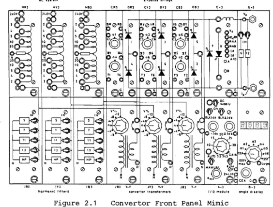
2.2 Convertor Model.
The central unit of the model is a 50 watt six-pulse bridge of modular design and its main constituent parts are illustrated in the front panel mimic diagram shown in fig 2.1 • The model has provision for both manual and automatic control. selected in module A3. which also contains the input and output signals used by the analogue predictive controller. The setting of the constant extinction angle controller is carried out in module B3 and the implementation of the automatic control in modules CR3-CY3-CB3 for red. yellow, and blue phases respectively. Alternative A, B, and C modules are available for an analogue based equidistant control scheme.
Analogue
Predictive T4
Controller T5
EDDC 1-+1f---:;;.. T6
L -_ _ _ --:;~::..J
Lo to Clear T1-6
(Lo to pre-set FPi)
Ti
block THi)
BLKA
(Lo to block all THis)
Figure 2.2
PreSet
S Q
Convertor Firing Circuit
+5V d.c.
Aux. Power
Firing K· I
Circuits Gj
ON/OFF
Level Detection
FPi III
Firing Pulses (monitored)
Detection
ON/OFF Logic Statesof THi
A block diagram of the valve firing circuits in the thyristor modules (module D) is shown in fig 2.2. Under predictive control the firing pulses FPi are produced in this module by means of a set-reset flip-flop driven by the Ti signals developed by the analogue controller. Blocking of individual valves or of the complete bridge can be achieved by the logic signals BLKi/ and BLKa/ respectively. Module D also produces the on/off states of the valves and their extinction angles EAi. Provision has been made for an external direct digital controller, under which the firing pulses are formed by a pair of logic signals PRi/ and CLRi/. External control is enabled by exerting the logic signal EDDC/ which disables the analogue trigger pulses.
The ac system impedance is simulated in module H by means of two variable reactors in series in each phase, with the central point connected to neutral through a shunt resistor which provides the desired impedance angle. The reactors are multiple tapped to provide a range of short circuit ratios (SCRs) between 2 and 20, which covers the range found in most practical schemes. This representation is only valid at the lower frequencies but is considered acceptable (Bowles, 1970) in the presence of ac harmonic filters.
Each phase of the model contains independently switchable filters for the 5th, 7th, 11th, and 13th harmonics well as a high pass unit for higher order harmonics. These filters are of the traditional type, with a single tuned arm for each of the lower characteristic harmonics.
Two sets of transformers (module J) are available to model the star-star and star-delta configurations and each transformer has several taps which can be used to unbalance the supply voltage. Care was taken with the design of these transformers to ensure that they have realistic leakage reactances, and one set was designed with a value of 5%, while the second set has a value of 8%.
The convertor can be transmission line model also
Microprocessor Sy~tem.
2.3.1 Introduction.
The aim of the project is to produce a microprocessor based HVDC development system to investigate possible applications of microprocessors to all aspects of HVDC transmission. The system would be required to provide full interactive facilities for program development, real time control operation, fault simulation, fault detection, and fault development control, and to provide comprehensive monitoring facilities to measure the performance of these sUb-systems. It was also considered desirable that the system, where possible, be constructed from standard 'building bloCks', and contain a minimal amount of dedicated specialised hardware.
With these requirements in mind it was first necessary to decide what type of microprocessor to use. The two main alternatives considered were whether to use a single very fast bit slice microprocessor or to use multiple general purpose processors and split the tasks between the individual processors. The following sections will deal initially with the factors influencing the final choice of processor and will then go on to describe the general structure of the overall microprocessor system.
Choice of Microprocessor.
2.3.2.1 Single or Multiple Processors.
A brief study of the requirements quickly indicated that if a single mi croprocessor were to be used, it would have to be extremely fast. The alternative was to use slower general purpose processors and split the tasks into groups that could each be handled by an individual processor in the time available.
The use of a singlec fast processor was quickly rejected for a
number of reasons, the major reason being that the processor would, on occasions, have to perform some tasks simultaneously. This would be incompatible with the inherent serial nature of a microprocessor. The general unavailability of peripheral support components and the lack of .high level programming languages also influenced the decision against the
Therefore the approach adopted was to split the tasks into groups with no simultaneous timing requirements and allocate one processor for each group. A preliminary allocation was made with one processor to handle the operating system and interactive communications, one processor to handle the data acquisition, one processor to handle the controller and one processor to handle fault detection.
2.3.2.2 Processor Size.
The next major consideration in the choice of processor was to decide whether to use an eight bit microprocessor or one of the newer more powerful, and more expensive, sixteen bit processors.
Initially a prototype system was built around two Intel iSBC 80/30 (Intel Manual e) single board computers which provided much valuable information.
An91e Measurement
Board
MULTIBUS
sac 30/30
Operator's Ter minal
...-_...J1d
AID
( onvertor Board
s Be 80/30
Figure 2.3 Prototype System
Firing
Pulses
This system was used to test the basic data acquisition algorithms and was also used to implement a prototype control system in order to ascertain the feasibility of a microprocessor based controller.
The major conclusion reached with the preliminary system was that a microprocessor implementation was feasible for the controller, although the
BOB5 was not a suitable processor to use. The problem is that the BOB5 has only a very limited sixteen bit instruction set and has no divide or multiply instructions of any kind. As most of the data to be processed consists of sixteen bit quantities, such as the timer values and the delay, commutation and extinction angles, and since it is necessary to perform multiplication as part of the control algorithm it was decided to use a suitable sixteen bit processor in the final HVDC development system. Possible processors included the Motorola 6Booo family, the Intel iAPXB6 family or the Zilog Z8000 family.
2.3.2.3 Departmental Support.
The final factor influencing the choice of processor was the facilities already available in the Department of Electrical and Electronic Engineering for both hardware and software development support.
For various reasons, primarily due to the different levels of product support in New Zealand available from the various manufacturers, the department uses the Intel family of microprocessor components, and has two Intel Series II Microprocessor Development Systems (Intel Manual d). These provide software support for the 80B5, 804B, 8051 and 8086 families of microprocessors, as well as hardware support in the form of In Circuit Emulators (Intel Manuals g,h) for the 8085, 8048 and 8086. Cross software for the B085 and B086 processors was also available on the department's VAX
11/750 computer.
2.3.2.4 Board Level Products.
For a microprocessor to be of any practical use, it must first be surrounded by various support components. To run a program it requires some memory, either ram or rom and to interface with the real world it usually requires some peripheral chips. To maintain the general nature of the processing elements it was deci ded that each mi croprocessor would be placed on a separate board with the necessary support components.
For the HVDe system it was envisaged that each processor would require at least one interrupt controller, several programmable timers, parallel I/O ports and probably a serial 1/0 port.
The memory requirements would be primarily determined by the anticipated size of the HVDe software. It was expected that the programs for the slave processors would be reasonably compact, but that the interactive routines would be relatively large. In addi tion it was known that the operating system under consideration would require up to 12K byte of rom and 140K byte of ram.
2.3.2.5 Bus structure.
It was considered desirable to have all processors operating on a common bus as this would permit the sharing of common resources such as global memory, dedicated data acquisition hardware and a disk controller. This requires that some form of bus access system be provided since each processor would require the use of the bus to communicate with the peripheral boards, and only one processor can use the bus at anyone time without conflicts arising.
The department was already using the Multibus (Intel Manual m) This has
Intel bus system known as the facility to provide the arbitration between the various processors, and Intel supplies a bus arbiter chip, the 8289 that interfaces the 8086 processor to the Multibus.
The Multibus permits up to three masters using a simple serial daisy-chain priority resolution scheme in which a processor may obtain access to the bus only if no processor higher in the chain is using it. If a slightly more complicated parallel priority resolution scheme is used then up to sixteen processors can be conveniently connected. This is the method that has been adopted for the HVDCdevelopment system, and it operates by providing each processor board with a bus request and a bus granted line. All request lines are applied to a priority encoding circuit which signals the highest priority processor currently requesting use of the bus to a decoder circuit which activates the appropriate grant line. The actual exchange of the bus between two processors is handled entirely by the 8289 bus arbitration chip.
The Multibus is capable of supporting both eight and sixteen bit data transfers and has a standard address space of sixteen megabytes.
2.3.2.6 Local Boards.
each board, and during assembly and subsequent testing several previously undetected design faults appeared. Considerable time was spent trying to fix these faults, ultimately with little success. In view of the poor results being obtained, it was decided to abandon them and purchase the necessary boards from commercial suppliers.
2.3.2.7 Commercial Boards.
A survey of possible boards indicated several that would fit the requirements, the final influencing factor being the use of Intel iSBC 86/12a (Intel Manual a) boards by other projects in the department. This board satisfied the memory requirements for the slave processors, containing up to 16K bytes of rom and 32K bytes of dual port dynamic ram.lt also provided the I/O functions needed with an eight level interrupt controller, three sixteen bit programmable timers, three eight bit parallel I/O ports and a programmable serial port. A total of three Intel iSBC 86/12a's were purchased for use as the slave processor boards. In order to meet the larger memory requirements of the interactive board, a Matrox MBC 86-12-128 (Matrox Manual) was obtained. This is functionally equivalent to the Intel iSBC 86/12a, but contains room for up to 64K bytes of rom and 128K bytes of ram, at least partially meeting the memory requirements of the operating system.
2.3.2.8 Newer Processors.
2.3.3 Support boards.
These boards provide the system with global resources accessible by all processors as opposed to the local resources that are located on each processor board. The support boards provided in the HVDe development system consist of two memory boards, one floppy disk controller board, and two data acquisition boards. The data acquisition boards comprise an analogue to digital converter board and an angle measurement board. The functions of these boards will be discussed in the following sections. Again, as was the case with the processor cards, general purpose commercial boards were used where possible in order to simplify design.
2.3.3.1 Memory boards.
It was considered imperative that no "instruction fetches" be performed through Multibus while the HVDe development system is running, as this would otherwise impose a prohibitively high bus usage, with a corresponding decrease in system speed. The 32K bytes of ram provided on each processor board available for the HVDe development system's use was considered adequate for the anticipated program size.
The monitoring system however requires a large amount of memory for data storage and so a 128K byte ram board was provided for this purpose. This was a board designed in the department, originally for the transient stability analysis project mention above. It is similar in operation to a number of commercial equivalents and provides 128K bytes of ram using 16K bit chips and also provides up to 16K bytes of eprom space. In addition to the monitoring system's storage space, the global data base was also placed on this board as it then made the database available to all processors at the same physical address.
This is a commercial board, an Intel SBC 056a (Intel Manual b). The use of this external memory board results in part of the operating system and all utility programs residing in off-board memory. The consequent drop in speed for the operating system is not considered to be important as, unlike the HVDC system, it is not required to respond to real time events.
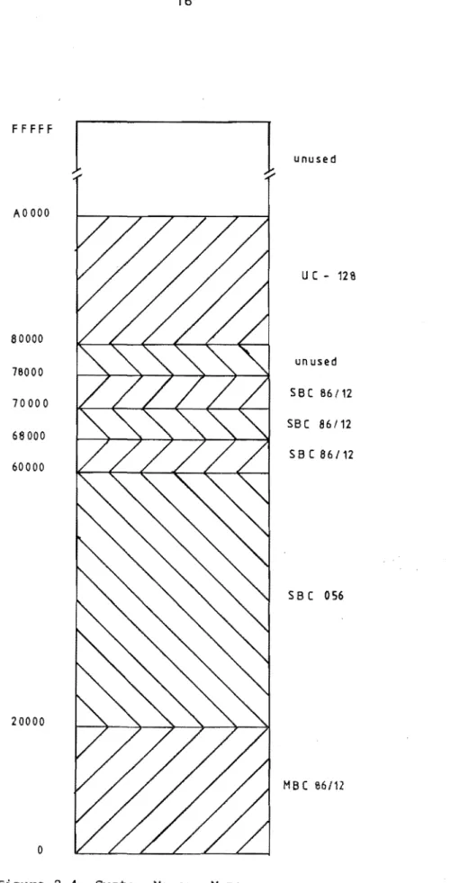
Fig 2.4 shows the memory map of the overall system. Note that because of the dual-ported nature of the memory, the slave processor memory that appears on Multibus in the address ranges 60000 67FFF, 68000 6FFFF,and 70000 77FFF also appears in the range 0 - 07FFF to the particular on-board processor.
2.3.3.2 Disk Controller.
FFFFF
1
1
unused AO 000u e - 12e
80000
unused 78000
S B e 86/12 70000
SBe 86/12
68000
S B e 86/12 60000
S Be 056
20000
MB
e
86/12o
.. ... _. -- .
~
--~-..
--.-
--------- - -- _... -.-~
2.3.3.3 Analogue to Digital Convertor Board.
An aid convertor board was built to meet the requirements that will be outlined in chapter ~.1.2. The major reason for building the board rather than using a commercially available one was that the multi-channel 12 bit aid convertor boards available in New Zealand contain only one aid convertor, and use an analogue multiplexer to select the channel to be converted. In this project however, it appeared to be desirable to be able to make several measurements simultaneously, for example dc voltage and current, or all 3 commutating voltage waveforms. Thus a board with eight individual aid convertors was designed.
The actual aid convertor chip used was the Analogue Devices AD57~K
(Analog Devices) This is a twelve bit microprocessor compatible convertor with a 30 ps conversion time. Twelve bit aid convertors were used for reasons explained in chapter ~ after experience with eight bit aid convertors in the prototype system. Fig 2.6 shows the block diagram of the board.
As shown , sufficient board space was available for eight aid convertors and their associated sample and hold circuits. The eight aid convertors were arranged as two groups of four, with the operation of each group being independent of the other, thus permitting different sampling rates to be used on each group. The aid convertor board occupies 32 locations in the ilo address space of the microprocessors.
1-'-1.0
I
I
I
I
j::!
'1 r- ,...- ~
(I) tv
.
0\
I
I
I
I
tJ:I
"
t:l r- i --0
a
;:l
~ '1
r1"
I
1
J
J
a
'1
g' (0
III
ntro I bus A
I
'10. control ,[ ogic
tIl gro up A
I-'
a 0
'"
(onversiont:l
1-'- complete
III
1.0 interr upt
'1 ~
I
inputs ~,...-I
r--J
data bus
data buffers and interfac e logi c
t}
MULTIBUS
I
J
-
-I
I
-
r-1
-
J
I
control logic group B
(onve.rsi on complete inter r upt
I
r--I
l-I
2.3.3.4 Angle Measurement Board.
The angle measurement board, shown in fig 2.7, contains a variety of hardware associated with the angle measurement process as well as other data acquisition hardware needed by the system. The actual operation of the angle measurement process will be described in the data acquisition chapter. This is the only board in the HVDC development system that is not of a general purpose nature, its design and operation being tailored to the specific application.
The first function the board provides is to buffer the signals from the HVDC convertor model. Fig 2.8 shows the buffer stages is detail.
analog to Z.CD
liP
to AID
Figure 2.8 Buffer Stage
The commutating voltages and dc voltage and current signals are first buffered and then attenuated before being level shifted and then applied to the aid convertor board. The incoming valve on/off state logic level signals are also buffered through schmidt triggers to improve the noise immunity.
rl~
system
I
cl oc k _I generator clockI 1
tl253
timer
L
voltages A I D
I
bufferI
( 0 nv ertor bo ardcrossing interrupt
r
-I
crossing zeroI
detectors
.-)'3 3
3 bi t tri-state ( omparator b u ffe r
{3
latch
I
data buffer and
Interfac e 10 gi c
}
MULTIBUS
-/
valve on/ off states
I
bufferI
/~
6 bi t
-
comparator{6
late h
data bus o%ff
interrupt
s
/
/6
tri state buffer
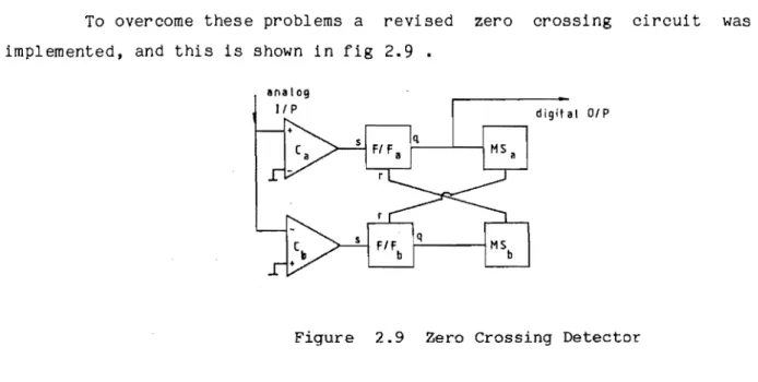
To overcome these problems a revised zero crossing circuit was implemented, and this is shown in fig 2.9 •
81'\alog
) I P digital O/P
Figure 2.9 Zero Crossing DetectDr
Two comparators are used to allow both the positive and negative gOing crossing to be detected individually. The outputs of the comparators are used to toggle the flip flops F/Fa and F/Fb to the set state, while the monostables MSa and MSb reset the flip flops as required. As shown the positive and negative halves are cross coupled so that the positive going transition is detected by comparator A and F/Fa is set. At the same time the setting of F/Fa triggers MSa which resets F/Fb and holds it in the reset state for approximately 170 degrees.
Thus if a multiple crossing occurs only the first positive going crossing is captured and subsequent crossings are ignored for the next 170 degrees. When the first negative going crossing, after the reset pulse is removed, is detected then F/Fb is set and a reset pulse applied to F/Fa, again for about 170 degrees. Therefore only the first crossing in the right direction is detected, and this must occur in a narrow window near the true crossing. If a commutation notch does occur in this window then the effective zero crossing detection point will shift, as shown in fig 2.10 , but only one crossing will be recorded.
waveform 1 squared I
output of fig 2.9
I I
~
I II
I II II I I
I I:
I~~
I
I I
~
Figure 2.10 Zero C~ossing Detector Waveforms
As described in chapter ~.3 the angle measuring hardware takes the form of two digital comparators which produce an interrupt whenever a transition of the valve on/off states or commutating voltages is detected. Associated with the two comparators is the 1.8 MHz system clock which provides the time of interrupt information, and is also supplied to the slave processor boards for other timing purposes. A 1.8 MHz clock was used as the system clock because it provided a basic timing interval of 0.01 degrees for a 50 Hz ac system. Fig 2.8 also shows the implementation of the system clock and digital comparators. The system clock has been implemented with an 822~ clock generator chip and an 8253 programmable counter timer chip. The digital comparators are implemented with 8131 bus comparator chips and the associated latches and tri-state buffers are standard TTL components. The exact mode of operation of the comparator and how i t is used in the angle measurement process will be descri bed in' chapter ~.3.2 •
Card Cage and Power Supplies.
The multibus card cages used as the backplane were the AMC 95/6~~0.
The power supply requirements for each board are tabulated below, with all currents in amps.
Supplies - +5v -5v +12v -12v +15v -15v +24v Boards.
SBC 86/12a 5.5 0.35 0.04
MBC 86/12-128 5.0 0.025 0.09
SBC 208 3.0
SBC 056 5.0
UC 128K 2.7 0.006
o.
1AID board 1.2 0.09 0.16
Angle meas 2.0 0.15 0.14
Disk drives 1.6 0.1 2.6
Totals. 37.0 0.106 1. 0.27 0.09 0.16 2.6
Commercial switch mode power supplies were used for all except the minus five volt supply in order to minimise the space required and the heat produced inside the cabinet. The minus five volt supply is regulated from the minus twelve volt supply by a three terminal regulator. The total supply rating available is shown below.
Supplies Available
-+5v 46.0
-5v 1.5
+12v 6.3
-12v 6.3
+15v 1.0
-15v
1 .0
+24v 3.2
Cooling for the supplies is provided by a total of three fans. In addition each of the card cages has a separate fan to ensure that sufficient air is kept moving across the surface of the boards. Finally the cabinet was designed so that the air exhausts over the disk drives, cooling them as well.
2.3.5 Terminal.
2.~ Conclusion.
3.0 Operating System and Software Support Facilities.
3.1 Operating System.
The requirement that the HVDC development system be capable of stand-alone operation requires that some form of operating system must be provided. This is needed to facilitate program development during the project and to permit software stored on floppy disks to be loaded into the microprocessors and executed. The exact choice of operating system was influenced by many factors, among them the languages supported, vendor supplied utilities, departmental support and the actual size of the operating system.
3.1.1 Choice of Operating System.
The basic requirement for the operating system was that it be capable of running on an 8086 microprocessor, be able to operate without needing a hard disk and be capable of providing the program development facilities required. This ruled out the use of a UNIX based system as these systems are very large and almost always require a large capacity hard disk to operate. The main choices appeared to be CP/M-86 from Digital Research , MS-DOS from Microsoft or RMX 86 from Intel .
CP/M-86 is a sixteen bit upgrade of the well known CP/M-80 operating system. Unfortunately there was relatively little information on it available here in New Zealand at the time the selection was being made, but from what information was available it appeared that it did not have compilers for a suitable high level language, and would not be easily interfaced to the HVDC programs.
Since the decision on the choice of operating system was made more information on both the above operating systems has become available, and the objections to their use at the time are no longer valid. Either could now be used, and both now seem to provide the required level of software development facilities.
RMX 86 (Intel Manual f) is Intels' real time multi-tasking executive for the 8086 microprocessor. As such it combined the facilities of a multi user operating system with a real time task scheduler. It had several advantages over the two other operating systems in that information was readily available on its capabilities and it was also already in use in another project in the department, with favourable results. It also provided compilers for Pascal, Fortran and PL/M-86, as well as an assembler and various utilities. Its drawbacks were its very large size, it requires about 140K byte of ram, and it needs a hard disk to function efficiently. Despite these drawbacks it was decided to use RMX 86 as the operating system since it was felt that the advantages outweighed the drawbacks.
3. 1 .2 RMX 86 Operating System Features.
This section is included to familiarise readers with some of the more important features of the RMX 86 operating system as it was implemented in the HVDC development system. More information can be found in reference "Introduction to the RMX86 Operating System".
As stated above RMX requires a hard disk to operate efficiently, it is however capable of operating with a pair of floppy disks, although this slows the speed of the compilers and other programs using the disk because the data transfer rates from a floppy disk are much slower than those that can be achieved from a hard disk.
More importantly, a library of simple interface routines is provided that permits a users program to be linked in to the operating system. These take the form of a number of procedures that may be called from a user program to access system resources. They permit a user program to, amongst other things, transfer data to and from disk files at any time. This has proved to be extremely useful since it allows data from the convertor captured by the microprooessor to be stored for permanent referenoe or subsequent analysis. There is, of course, a trade-off. Use of the libraries requires that extra code be linked to the user program, resulting in more memory space being required to run it. Compared with the advantages offered this is only a very minor problem.
Finally the most important feature of RMX is that it is user configurable. That is the component parts are supplied with a number of user selectable options. The user then builds an operating system by selecting the features he requires. This permits the customising of RMX to fit any target system. RMX does make some assumptions about the hardware available, only Intel made support components are accepted, and must be used. This is not a problem although the processor that runs the operating system is a Matrox MBC 86-12-128, as this has all the required support components.
3. 1 .3 Overheads Imposed by the Operating System.
RMX 86 is intended as a real time multi-tasking executive program and as suoh is capable of scheduling tasks to run in response to external real-time stimuli. In practice, the time taken to switch tasks through the operating system is too long and this feature is not used by the HVDC system programs. The size of the operating system also provides another maj or over head.
programs. This in turn means that the whole of RMX cannot fit in the remaining memory space, and the overflow is contained on an external 256k byte ram card. The remaining space on this card is not used by the HVDC system, but is reserved for the use of the RMX 86 compilers and utilities.
By partitioning the memory space in this way into separate areas for the operating system and the HVDC system it is possible to switch between running one or the other without corrupting the code of either. This speeds development and debugging of the HVDC system, but requires more memory than would otherwise be needed.
3.2 Languages.
The choice of language is constrained by the operating system chosen, but the final choice made is still of great importance as it will directly affect the execution speed of the HVDC programs.
3.2. 1 Choice of Languages.
3.2.2 Features of PL/M-86.
PL/M-86 is described by Intel as an application language. It provides the structured, modularised, procedure orientated advantages of a high level language while still allowing the programmer to communicate with specific memory and i/o resources when necessary. It supports basic arithmetic functions for unsigned eight and sixteen bit numbers, as well as for sixteen bit signed integers and thirty two bit floating point numbers.
The compilers for PL/M-86 provided by Intel also offered several advantages. The object modules produced can be combined together with those produced from assembly language sources and the compiler has built-in optimisation features that result in the compiled code being little longer than the code that would be produced from assembly language. Experience has shown that a PL/M-86 implementation of an algorithm produces only about 25% more code than the equivalent assembly language implementation, and has a correspondingly longer execution time. This overhead is a small price to pay for the much increased speed of code generation that the use of PL/M-86 offers.
3.3 Software Development Techniques.
Where ever possible a structured approach has been adopted for the development of the HVDC software. All interactive programs are written as small modules containing only one or two procedures. These modules are then combined by the linker to form the executable program. This permits easy expansion and'testing of code as changes from one step to the next can usually be confined to a single module.
4.0 Data Acquisition Sub-System.
All the sub-systems that are described in this thesis will only operate correctly i f the data supplied to them is both accurate and up to date. Thus the operation of the data acquisition SUb-system is of vital importance to the successful operation of the entire HVDC development system. This chapter starts by describing the data requirements of each of the maj or sub-systems and then proceeds to descri be how these requirements ha ve been met.
4. 1 Sub-system Data Acquisition Requirements.
4. 1 • 1 Control Sub-system. ,
The data required from the convertor for the control system consists primarily of the dc line current, the minimum delay and extinction angles recorded during the previous cycle and, when operating in constant extinction angle mode, the value of each valve'S extinction angle recorded during the previous cycle.
Values of minimum delay and extinction angle can only be updated at each valve turn-on or turn-off whereas the dc current is a continuously varying quantity. and the most up to date value should be used. In practice there is always a small delay between the instant when the value was measured. and when it is used in the control calculation. and this may have a detrimental effect on controller accuracy. The use of separate control and data acquisition processors minimises this effect however, as the value may be updated by the data acquisition processor during the course of the control calculations.
4. 1 .2 Fault Simulation and Detection SUb-systems.
Unlike the control sub-system the fault simulation sub-system requires relatively little information from the convertor. The data required being limited to the commutating voltage zero crossing instants, which are required to synchronise the operation of the fault simulator with the convertor. As tn the case of the control sub-system, detailed data is required from the operator in order to specify the fault condition to be simulated and, again, provision has been made for this in the interactive software. As will be described in chapter 6 the fault simulation tasks are
actual~y run on the control processor. Since the fault simulator must respond instantly to each zero crossing interrupt, the fault simulator's data acquisition task is also run on the control processor.
The fault detection sub-system, which is totally independent of the fault simulation sub-system, requires the convertor valve turn-on and turn-off sequences and the controller firing pulse sequences. The data acquisition task to provide the on/off sequences is run on the fault detection processor. This has been done to ensure that the information is available to the fault detection task as quickly as possible.
4. 1 .3 Interactive Analysis Sub-system.
~.2 Conventional and Storage Modes.
The data acquisition process being described is capable of producing extremely large quantities of data. In an attempt to reduce this data to a manageable size, during normal operation only the data captured during the most recent cycle is stored. During fault simulation or whenever a major controller parameter is changed the amount of data needed by the analysis package is substantially increased. Instead of over writing the data values as the new values become available and discarding the data buffer entries as they are processed, all information is transfered into a special data base.
This operation is triggered by the fault simulation or control sUb-systems several cycles, the exact number being set by the operator, before the event takes place. Detailed recording continues for about twelve cycles after being triggered. In this way a complete record of the convertor's operation from before the event occurred until recovery is complete is obtained.
This enhanced operation has the disadvantage that a large amount of data is produced, typically in excess of 5DK bytes, and this is why recording in this mode is limited to twelve cycles.
~.3 Convertor Angle Measurement.
From the data acquisition requirements listed above it is apparent that the measurement of delay, commutation and extinction a,ngles are of major importance.
Detection of On/off and Zero Crossing Instants.
manner.
In each case the instant of transition is determined in a similar The incoming signals are applied to one side of a digital comparator, either three or six bits wide, and are also made available to the microprocessor through a corresponding data port. On the other side of the comparator a set of latches hold the states measured after the last transition. Thus while the inputs remain unchanged the comparator has identical sets of inputs and indicates this equality on its output. When one or more input lines change the equality is removed and the change in comparator output generates an interrupt for the data acquisition processor. The processor immediately responds by reading the new input states and writing them back to the latch. This restores the equality and removes the interrupt request.
As well as the data acquisition processor, the fault detection and control processors are also interrupted by the on/off and crossing transitions. This permits the fault detection and fault simulation software to obtain the information required. The response to these interrupts will be covered in the appropriate chapters.
4.3.2 Data Acquisition Interrupt Service Routines.
Fig 4.1 shows the structure of the service. routine.
Data Acquisition Interrupt
Save La tc h
Reljlsters Time.r
Read Data
and
Write to Latch to Stack
Figure 4.1 Data Acquisition Interrupt Routine
The new valve conduction state is then read from the appropriate data port and immediately written back to the comparator on the angle measurement board to clear the interrupt request. The data is then placed onto the top of a circular buffer together with the time and a byte identifying the buffer entry as coming from a valve on/off event.
A virtually identical interrupt service routine is run in response to the crossing interrupts, except that the identification byte in each buffer entry is changed. The same buffer is used by both routines and this consequently contains a record of convertor activity in chronological order.
Processing in the interrupt service routine has been deliberately kept to a minimum in order to keep the interrupt service time as short as possible. This is necessary because once one interrupt occurs it is not possible to respond to a subsequent interrupt without losing data until the first has been processed. Thus if a zero crossing was quickly followed by a valve switching then the time recorded for the switching will be increased by the length of time taken by the crossing interrupt service routine. This can introduce a small error into the measurement process.
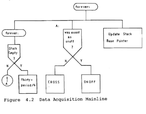
4.3.3 Angle Calculation.
The buffer entries are cleared by the data acquisition main line program which runs whenever an interrupt is not being serviced. Each entry in the data buffer consists of four bytes, the first is used to identify the data following as coming from either a crossing interrupt or a valve on/off interrupt. The next byte in the entry contains the new crossing or valve conduction state, depending on the source, and the final two bytes contain the time at which the interrupts occurred. The entries are decoded and a corresponding angle is calculated.
will also be stored and used to determine the extinction angle for valve V5 when the next crossing C4 is detected. Thus at each turn-on a
corresponding delay angle is calculated, at each turn-off a corresponding commutation angle is calculated and at each zero crossing a corresponding extinction ang~e is calculated. Fig 4.2 shows the structure diagram for the mainline routine that performs this task.
Data Acquisition Mainline
Stack
Empty 7
period/I>
A:
CROSS
IIlIS event
an
onoff
?
ON OFF
Update Stack
Base Pointer
Figure 4.2 Data Acquisition Mainline
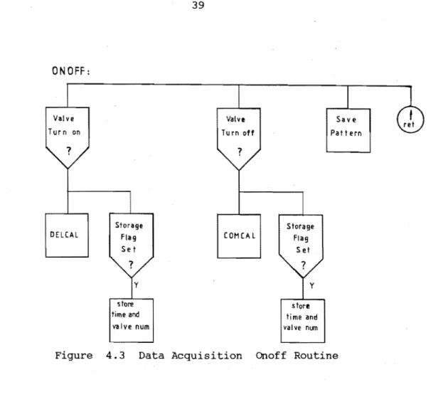
As each new entry on the data buffer is detected, the first byte is examined and either the crossing routine or the on/off routine is called to process the entry. Fig 4.3 shows the operation of the on/off routine.
ON OFF:
Valve
T ur n on
?
o nCAl
Storage Flag Set
time and valve nurn
Valve Tu rn off
?
[OH[Al Storage Fla9 Set
time and
valve num
Figure 4.3 Data Acquisition Onoff Routine
Once a turn-on has been positively identified, a subroutine is then called to calculate the delay angle associated with the tUrn-on. This is subroutine Delcal and its operation is shown in fig 4.4 .
DELCAL:
Calculate
nell a
an d stor
Find new
min a
and store
S ave nell a in array!cntl
Storage Flag
set
cnt
>= max
y
Reset Storage
F1a9
Data Acquisition Delcal Routine Figure 4.4
On returning to the on/off routine at the completion of Delcal, the storage mode flag is re-examined and if it is set the time that the turn-on occurred and the number of the valve in which the turn-on occurred are also saved for subsequent analysis.
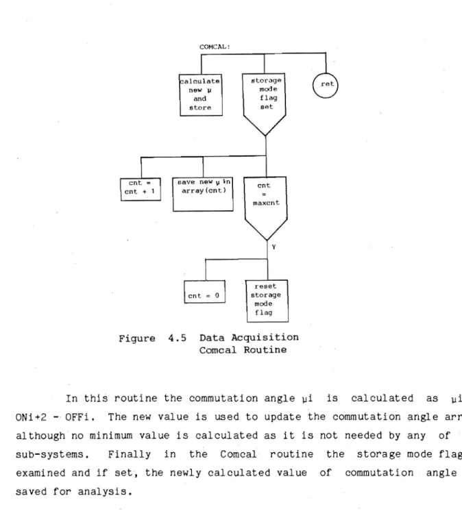
COMCAL:
new II
and
store
save neW \I In
array (cntl
storage
mode
flag set
ant
maxcnt
y
reset
storage
mode
flag
Figure 4.5 Data Acquisition
Corneal Routine
In this routine the commutation angle ~i is calculated as ~i
ONi+2 - OFFi. The new value is used to update the commutation angle array, although no minimum value is calculated as it is not needed by any of the sUb-systems. Finally in the Comcal routine the storage mode flag is examined and i f set, the newly calculated value of commutation angle is saved for analysis.
Again, on return to the on/off routine the storage mode flag is re-examined and if it is set then the turn-off time and the valve number are also stored for analysis. Finally the on/off routine stores the new conduction pattern for use next time before returning to the main line. The mainline then completes by updating the buffer pointers before waiting for the next entry to occur.
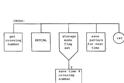
CROSS:
get crossing
number
EXTCAL
storage mooe flag set
save time & crossing number
save pattern for next
time
Figure 4.6 Data Acquisition Cross Routine
The crossing number is identified in mUGh the same manner as were the valve numbers, and the time of the crossing is transferred from the data buffer to the crossing time array. The routine Extcal is then called to calculate the corresponding extinction angle and this is shown in fig
4.7 .
EXTCAL:
and
store
new
min
slorilge mode flag set
y
cnt
maxcnt
y
. - - - 1
reset storage
mode flag
Data Acquisition Extcal Routine
Figure 4. 7
4.4 Direct Current Measurements.
As described in section 4.1.2 the dc current is required by the control software and can also be used by the monitoring system. The signals supplied from the convertor are analogue voltages and so some form of analogue to digital conversion is needed before they can be processed by the microprocessor.
AID Timer Interrupt
Rave
register
latch sample &
hold
restart timer
start AID onvertor
restore egisters
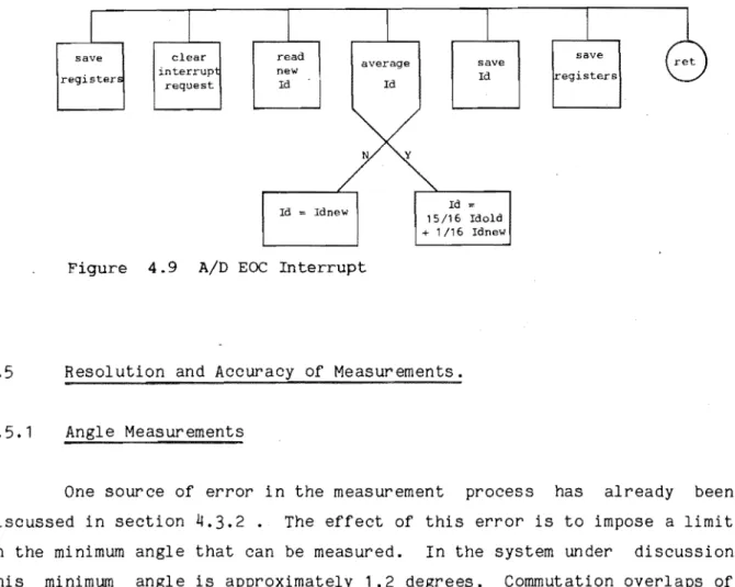
Figure ~.8 AID Timer Interrupt Routine
A second interrupt occurs when conversion is complete and the response to this is shown in fig
4.9 ..
The interrupt request flip flop is cleared and the values read in and stored in memory. Two options are provided, the value stored in memory can be either the value read directly from the aid convertor or can be the average of the last sixteen measurements. The option to be used is selected by the operator and may bechanged during operation.
4.5. 1
AID EOe Interrupt
saVe
register
clear interrup
request
read new Id
Id Idnew
average Id
Figure 4.9 AID EOC Interrupt
save
Id
Id '"
15/16 Idold
+ 1/16 Idnew
Resolution and Accuracy of Measurements.
Angle Measurements
save
egisters
shorter duration appear as zero degrees since the turn-on and turn-off appear to have occurred simultaneously. The delay and extinction angles are only affected over a small range of values about the 0, 60, 120, and 180 degree points, and as operation near these points is not usual under normal operating conditions the problem is not serious. Even when it does appear the effect is merely to increase or decrease the angle by no more than 1.2 degrees.
The resolution of the measurement is determined by the system clock. Since a sixteen bit timer was the largest convenient size available, the maximum frequency that can be used is limited to 6.55 MHz. If a higher frequency is used then the timer will overflow and wrap around before the end of the cycle. If this occurs a large angle will be measured incorrectly as having a much smaller value.
In this system a frequency of 1.8MHz is used, which has the advantage that each 'tick' is of 0.01 degrees duration for a 50 Hz system, and the values obtained by the angle measurement routines may be conveniently displayed without further conversion. The values of the angles are only displayed to one decimal place and so any fluctuation of the display is due to fluctuations in the convertor and is not a result of limited resolution.
4.5.2 DC Current.