Electrostatically defined quantum dots in a two dimensional
electron/hole gas at the Si and SiO
2interface
M.W.S. Vervoort
University of Twente
Department of Electrical Engineering Institute for Nanotechnology
Nano Electronics
Electrostatically defined quantum dots in a two
dimensional electron/hole gas at the
Si
and
SiO
2interface
M.W.S. Vervoort
1. Supervisor
PhD S.V. Amitonov
Group: Nano Electronics University of Twente
2. Supervisor
dr.ir. F.A. Zwanenburg
Group: Nano Electronics University of Twente
3. Supervisor
prof.dr.ir. W.G. van der Wiel
Group: Nano Electronics University of Twente
Reviewer
prof.dr. J. Schmitz
Group: Semiconductor Components University of Twente
M.W.S. Vervoort
Electrostatically defined quantum dots in a two dimensional electron/hole gas at the Si and
SiO2interface
April 12, 2017
Supervisors: PhD S.V. Amitonov, prof.dr.ir. W.G. van der Wiel, dr.ir. F.A. Zwanenburg and
prof.dr.ir. W.G. van der Wiel
Reviewer: prof.dr. J. Schmitz
University of Twente
Nano Electronics
Institute for Nanotechnology
Department of Electrical Engineering
Drienerlolaan 5
Abstract
In this thesis electrostatically defined quantum dots formed in a two dimensional electron/hole gas are investigated. Until now, only quantum dots have been made in intrinsic silicon by accumulating charge carriers while in this project the main focus is on defining a quantum dot by means of depletion.
The devices used in this thesis are made from a Si−SiO2−Al2O3 layer stack with a
metal gate on top. At the interface of SiO2−Al2O3 negative fixed charge is present
attracting free holes at the Si−SiO2 interface, acting as a two dimensional hole gas.
These holes are spatially confined into a quantum dot with the use of metal gates. By making use of literature, device iterations and a finite element method simulation, a close to optimal depletion hole dot design is presented. This depletion hole dot made from palladium is shown to be stable with transport measurements up to the possible few hole regime.
As an alternative to palladium this thesis addresses the possible implementation of titanium as a gate metal. Where titanium has the advantage of being more robust during processing thereby increasing device yield, but on the contrary it is found to affect the negative fixed charge in the system.
Additionally a charge sensor is implemented by fabricating a double layer device made entirely from titanium. This sensor is a single electron dot shown to be stable over more than 30 charge transitions. This, and the fact that titanium is not found
to oxidize after a cumulative time of 95 minutes at 160◦C indicates that titanium is
a good alternative for palladium.
Furthermore this thesis shows that it is possible to define both a depletion hole dot and single electron dot simultaneously in gate space allowing the device to be pushed even further by using charge sensing.
1
Acknowledgments
First of all I would like to thank Floris Zwanenburg and Wilfred van der Wiel for the lectures during my masters in the subject of nanoelectronics, the intriguing field and their combined enthusiasm convinced me to pursue this field during my thesis. Their devotion is shared by my day to day supervisor Sergey Amitonov, who I would like to thank for his extensive knowledge, guiding and helping hand in the cleanroom, as well as in the lab. Following him like a shadow in the first phase of my thesis was very interesting and made me learn a lot about processing. Additionally to the cleanroom work he supported me like a call center on Slack, and even when he was not at the office he out-competes my girlfriends response speed.
Besides this already great team of supervisors I would like to thank Chris Spruijten-burg for joining when the original project came to a standstill due to the failure of an essential machine in the cleanroom. You helped me in search for a new topic and showed me the way to electrostatically define quantum dots.
Furthermore I would like to thank Floris and Matthias for their involvement in the keeping students slim and fit policy called: "NE football team". It was a pleasure to defend the honors of NE against others. Besides my direct supervisors I would like to thanks my fellow students and other PhD’s for giving me a helping hand when needed with EBL sessions, measurements, sharp remarks and mental support. Of course also many thanks to Thijs and Joost for their help with the Oxford Heliox setup.
Many thanks also go to Jurrian Schmitz who was has made major contributions for my master program by arranging not only an internship at Philips Research but also being the external member of my graduation committee. I learned a lot from his feedback and enthusiasm regarding projects.
For the support throughout this thesis and for the delighted talks about what the hell I am actually doing I would like to thank my family, friends and Lotte who were a major support throughout this thesis.
To conclude all other members of the Nanoelectronics group who made the stay all the more enjoyable, many thanks to you all!
Contents
1 Acknowledgments vii
2 Introduction 3
2.1 Aim of this research . . . 4
2.2 Thesis outline . . . 5
3 Theory 7 3.1 Silicon . . . 7
3.2 Quantum dot . . . 9
3.3 Coulomb interactions . . . 9
3.4 Coulomb diamond . . . 13
3.5 Double quantum dot . . . 15
3.6 Charge stability diagram . . . 16
3.7 Charge sensing . . . 18
3.8 Fixed charge . . . 20
4 Simulation 23 5 Device layout 25 5.1 Microscale device . . . 25
5.2 Ten gate depletion dot . . . 26
5.3 Ciorga design . . . 26
5.4 Single hole and single electron dot . . . 27
6 Experimental methods 29 6.1 Electron beam lithography . . . 29
6.2 Cold development . . . 29
6.3 Metal deposition . . . 30
6.4 Lift off . . . 30
6.5 UV ozone . . . 30
6.6 Experimental setup . . . 31
7 Results 35
7.1 Ten gate depletion dot . . . 35
7.2 Electron accumulation and hole depletion dot . . . 37
7.3 Ciorga design . . . 39
7.4 Minimal single hole and single electron dot . . . 42
7.5 Fixed charge . . . 53
7.6 Palladium and Titanium gates . . . 55
8 Conclusion and discussion 57 9 Outlook 59 A Appendix 61 A.1 Experimental Methods . . . 61
A.2 Process flow . . . 61
A.3 Simulation . . . 63
A.4 Results . . . 65
Tab. 1.1.: Abbreviations used in this thesis.
Symbol Description
2DEG Two-Dimensional Electron Gas
2DHG Two-Dimensional Hole Gas
AFM Atomic Force Microscope
BG Barrier Gate
CI Model Constant Interaction Model
DAC Digital to Analog Converter
DMSO DiMethylSulfOxide
DOS Density Of States
EBL Electron Beam Lithography
FEM Finite Element Method
GPIB General Purpose Interface Bus
IPA IsoPropyl Alcohol
LG Lead Gate
MIBK Methyl IsoButyl Ketone
NE Nano Electronics
PCB Printed Circuit Board
PMMA PolyMethyl MethAcrylate
QTLab Quantum Transport Laboratory
SD Source drain
SET Single Electron Transistor
SHG Second-Harmonic generation
SHT Single Hole Transistor
SMU Source Measure Unit
UV UltraViolet
ZIF Zero Insertion Force
Tab. 1.2.: Constants used in this thesis.
Symbol Description Value Unit
e Elementary charge 1.602·10−19 C
kB Boltzmann constant 1.38·10−23 m2 kg s−2 K−1
h Planck constant 6.626·10−34 m2kg s−1
Tab. 1.3.: Symbols used in this thesis.
Symbol Description Unit
C Capacitance of the dot F
CD Drain capacitance of the dot F
CG Gate capacitance of the dot F
CS Source capacitance of the dot F
Eadd Addition voltage eV
Ec Conduction band eV
EC Orbital level energy eV
EF Fermi level eV
EFi Intrinsic Fermi level eV
Ev Valance band eV
∆E Charging energy eV
ISD Source drain current A
Rt Tunneling Resistance Ω
T Temperature K or◦C
VSD Source drain voltage V
µS Electrostatic potential of the source eV
µD Electrostatic potential of the drain eV
2
Introduction
The prediction of Gordon Moore in 1965 that the number of transistors in a dense integrated circuit would continue to double every two years led to a business model of miniaturizing in the semiconductor industry [1]. When these transistors cramp up closer to the fundamental limits of physics it becomes interesting to note that after being scaled down a couple orders of magnitude in size no major changes in behavior occur. However, this behavior does change when sizes become in the order of the electron wavelength and physics as we experience it in daily live changes. A new and novel concept is needed to gasp these changes and to apply them for new technology. To do this physicist leap into the field of quantum mechanics where the behavior of matter and its interactions with energy on the scale of atoms and subatomic particles is investigated. As Feynman already noted in 1959: "There is plenty of room at the bottom" [2].
In the field of quantum mechanics one could think of an atom connected by source
and drain contacts where the quantization of charge in units of "e" becomes
impor-tant, a so called quantum dot. A quantum dot is an artificially fabricated device in a
solid, typically consisting of103−109atoms and a comparable number of electrons.
These electrons are virtually all tightly bound to the nuclei of the material, however some free electrons between one and a few hundred can reside on the dot [3].
To form a quantum dot the energy spectrum has to be confined in all three directions leading to quantum effects that strongly influence the electronic transport at low temperatures. In particular it leads to the formation of a discrete energy spectrum. The atomic state of a quantum dot can be probed by attaching current and voltage leads enabling movement of electrons on or off the dot at the cost of the charging en-ergy required to overcome the Coulomb repulsion between electrons [4]. Whenever a single quantum dot is properly understood one could look into systems of coupled dots, a so called artificial molecule. Two quantum dots can be coupled by weak ionic bonds or strong covalent bonds where the two dots are quantum-mechanically coupled. This coupling allows an electron to tunnel between the states of both dots, thereby creating a coherent wave that is delocalized over the two dots, hence a superposition state. A so called qubit [5].
A qubit behaves fundamentally different from a classical bit (0 or 1) and was first posed by Yuri Manin in 1980 [6]. It makes use of the superposition of two eigenstates in a linear combination as depicted in Equation 2.1. Realization of a qubit is possible
in many ways as in principle any quantum two-level system can be used, as for example nuclear spin [7], single photon by using the polarization of light [8], by using electron spin or hole spins. At the moment these realizations of qubits are unfortunately less stable than regular bits due to scattering effects causing loss of spin coherence.
|ψ >=α|0>+β|1> (2.1)
Advances in silicon qubits are being made by using isotropically purified silicon 28 containing zero magnetic spin limiting the effect of hyperfine interactions and spin orbit coupling [9], [10]. Whenever these qubits are better understood and spin coherence times are further improved they are a good candidate for building blocks of a quantum computer.
A quantum computer makes it possible to efficiently solve certain computational problems which have no efficient solution on a classical computer, e.g. prime fac-torization of an integer [11]. Another example that demonstrates the power of the quantum computer is the search through unsorted data [12].
To fabricate these computers better understanding of quantum effects and possible ways to define quantum dots are however required for which this thesis will deliver a small building block.
2.1 Aim of this research
The aim of this thesis is to measure the few or even single hole regime of a lateral depletion hole dot in intrinsic silicon. These dots are electrostatically defined artificial
quantum dots in a two dimensional electron gas at the Si-SiO2 interface. The devices
2.2 Thesis outline
The outline of this thesis is as follows, sorted per chapter with a brief description:
Chapter 3, Theory
This thesis starts with the important properties of silicon for quantum applications followed by electron and hole transport in traditional semiconductor devices. Sec-ondly the concept of a quantum dot is addressed involving spacing of the energy levels, Coulomb interactions, tunneling rates, excited states, capacitive coupling and fixed charge.
Chapter 4, Simulation
This chapter addresses the setup and results from the finite element method simula-tions made by using Comsol Multiphysics. Additionally import straight from KLayout into Comsol Multiphysics as well as importing atomic force microscope scans are discussed.
Chapter 5, Device layout
In this chapter the layout of several samples that were fabricated during the iterative process in this thesis are discussed.
Chapter 6, Experimental methods
Experimental methods including cleanroom techniques such as the electron beam lithography, cold development, lift off, ultraviolet ozone exposure, measurement preparation and the experimental setup are discussed.
Chapter 7, Results
In this chapter the results presented for the different types of devices as well as measurements about the fixed charge in the system, and possible implementation of palladium and titanium as a gate metal.
Chapter 8, Conclusion and discussion
In this chapter the results from this thesis are discussed and conclusions are drawn.
Chapter 9, Outlook
To conclude an outlook is presented addressing new insights and questions arisen during this thesis. These statements and ideas can act as a guideline for further work and hopefully lead to the publication of a paper in the near future.
3
Theory
In this section the theory concerning this thesis is discussed starting with classical semiconductor physics such as silicon devices and band structures to quantum mechanical behavior including Coulomb interactions, quantum dots, excited states and charge sensing. To conclude the origin of fixed and mobile charge in the system are discussed.
It is noted that the measured devices mainly address transport of holes while some graphical representation in the theory section address transport of electrons. These representations are more intuitively and therefore it will be clearly stated whether an illustration applies to either hole or electron transport.
3.1 Silicon
The most common material in the world of solid state physics and second most abundant on earth, after oxygen [13], is silicon which has a wide variety of uses due to its properties as a semiconductor material.
Silicon orientates itself as a diamond cubic crystal structure since it crystallizes in the same pattern as a diamond, hence Figure 3.1a [14]. Purified silicon consists
of three stable isotopes: 28Si, 29Si, 30Si, respectively being 92.2, 4.7 and 3.1 %
of the total amount of atoms [15]. From these stable isotopes,29Si has a natural
+12 nuclear spin creating an inhomogeneous and randomly fluctuating background
of spins decreasing coherence times and offering less control of the system. To
overcome this problem enriched28Si wafers beyond 99.9998 % are being fabricated
for semiconductor quantum devices [16].
In intrinsic silicon the number of holes and electrons available for transport are equal (p = n) because silicon has no overall net charge. This results in the intrinsic
Fermi level (EFi) being equally spaced between the valence (Ev) and conduction
band (Ec) where the band gap is determined by the lowest point of the conduction
band and the highest point of the valence band. Monocrystalline silicon is an in-trinsic semiconductor with an indirect band gap between the valence band and the
conduction band ofEg = 1.12 eV atT = 300 K as depicted in Figure 3.1a. The band
gap differs from material to material and is largest for insulators where almost no charge transport is possible because electrons are tightly bound to the nuclei, up till
(a)
(b)
Fig. 3.1.: a) Face-centered cubic structure of a silicon unit cell [17]. b) Energy band diagram of monocrystalline silicon,Egis the energy band gap [18]
metals where the conduction and valence band overlap enabling charge transport between atoms.
With a semiconductor material such as silicon these bands can be tuned by doping the intrinsic silicon with a substitutional atom that has nearly the same size and a unit valence of plus one (n-type/Arsenic) or minus one (p-type/Boron). These substitutional atoms act as dopants shifting the Fermi level closer to the valance (p-type) or conduction (n-type) band. Due to this valence difference free electrons or holes become available in the valence band allowing an electron/hole to move from one atom to another. The amount of electrons available for charge transport
is not only influenced by doping but also due to thermal energy (kB T) allowing
electrons and holes to move from one energy state to another. The probability of occupying an available state can be calculated from the Fermi-Dirac distribution as depicted in Equation 3.1 [19]. Some electrons occupy an energy state higher
than the Fermi energy (E > EF) due to thermal energy creating free electrons in
the conduction band allowing the metal to conduct. When the thermal energy is decreased by using for example a cryostat, the electrons redistribute under the Fermi
energy (E < EF) disabling transport between atoms, because the conduction band
is empty and the valence band completely filled at zero temperature. Besides the Fermi energy the free carrier concentration depends on the Density of States (DOS) describing the number of states per interval of energy at each energy level is allowed.
f(E) = 1
e E−EFi
k
BT + 1
3.2 Quantum dot
A quantum dot is an artificially structured system that can be filled with electrons or holes by confining the energy spectrum in all dimensions. A particle that can move freely in two directions, but is confined in one direction is called a quantum well. Accordingly a particle that is confined in two directions is called a quantum wire and a particle that is confined in all directions a quantum dot. It leads to the formation of a discrete (0D) energy spectrum.
A quantum dot typically consisting of103−109 atoms and a comparable number of
electrons/holes tightly bound to their nuclei has however some free electrons/holes (between one and a few hundred) that can reside on the dot or so called island [3]. This island is coupled to a source and drain through tunnel junctions and capacitively to one or more gate electrodes as schematically depicted in Figure 3.2a. By tuning these tunnel junctions and gates into the Coulomb blockade regime electrons and
holes can tunnel on or of the dot in units of ’e’ allowing for the formation of a
single-electron or single-hole transistor (respectively SET, SHT) [9].
(a)
(b)
Fig. 3.2.: a) Schematic representation of a lateral quantum dot in the shape of a disk connected to source and drain, and capacitively coupled to the gate [3].
b) Simplified electrical equivalent of a lateral quantum dot system with source and drain contacts connected by a tunnel junction to the island, and a gate capacitively coupled to the dot. The tunnel junction is equivalent to a resistor and capacitor in parallel as depicted at the left top [20].
3.3 Coulomb interactions
Transport in a quantum dot takes place due to Coulomb interactions describing the force that interacts between static electrically charged particles present on the island and the source/drain. This indicates that a certain Coulomb repulsion (preventing an electron to flow) has to be overcome in order for an electron to tunnel on or off the dot. In literature this effect is known as Coulomb blockade since no current can flow through the device and was already first noticed in 1987 by Fulton et
al. [21]. Coulomb blockade can be represented by drawing the energy levels of
the source (µS), drain (µD) and dot (µdot) schematically as depicted in Figure 3.3a
where the energy potential of the dot does not align with the bias window. The blockade can be overcome by increasing the potential between the source and drain or alternatively by changing the voltage on the gate. Due to capacitive coupling
of the gate the potential landscape alters and the available state (µN) allows an
electron to tunnel in and out of the dot as depicted in Figure 3.3b.
(a) (b)
(c)
Fig. 3.3.: Schematic representation of the electrochemical potential levels of a quantum dot in the low bias regime regime for the case of electron transport. a) No energy level of the dot falls between the bias window, meaning an electron can tunnel into the N-1 state when empty but cannot tunnel off the dot to the drain, hence Coulomb blockade. b) The energy level of the dot falls between the bias window allowing an electron to tunnel into the N state and tunnel forwards onto the drain, so the number of electrons can alternate between N-1 and N, resulting in a single-electron tunneling current. The magnitude of the current depends on the tunnel rate between the dot and the reservoir on the leftτSand on the rightτD. c) Schematic representation of the current through the dot as a function of gate voltageVG. The gate voltages where the level alignments of (a) and (b) occur are indicated by the arrows [9].
A quantum dot can be described in the electrical domain by using the constant-interaction (CI) model. This model assumes that Coulomb constant-interactions between an electron occupying the dot and all other electrons (inside and outside the dot) are parametrized by a constant capacitance C. This model is hold valid if given that the quantum dot is an almost isolated system and secondly, the energy levels of the dot are independent of the number of electrons on the dot [22]. The total capacitance of
The energy potential of a quantum dot can be described by Equation 3.2 whereEN
is the sum over the occupied single particle energy levels. And the left part is the continuous classical potential due to capacitive coupling of a bias voltage applied from the source/drain and the gate to the dot [23].
U(N) = [−|e|(N −N0) +CSVSD+CGVG]
2
2C +
N
X
n=1
EN (3.2)
µdot(n) = (N −N0−1/2)EC−e(CG/C)VG+EN (3.3)
This discrete behavior due to Coulomb blockade is depicted in Figure 3.3c where the
addition energy (Eadd) has to be paid to add an additional electron to the dot. In
general the addition energy is equal to the charging energy (EC) except for when an
extra penalty has to be paid whenever a shell is filled and the electron has to go into a new orbital. Each orbital state can be occupied by a certain number of electrons following Hunds rule and the Pauli exclusion principle. This means that in case of adding an electron to a new orbital both the charging energy and the orbital level
spacing (∆E) have to be provided, hence Equation 3.4.
Eadd=EC+ ∆E =
e2
C + ∆E (3.4)
This indicates that to overcome Coulomb blockade the bias voltage moving an electron on or off the dot must be higher than the elementary charge divided by the
self capacitance of the island, henceVbias> eC2. Besides this, two other requirements
to form a quantum dot have to be met:
1. As a first requirement the electron should be able to reside on the dot, therefore
the charging energy (Ec) must be larger than the thermal energy: kBT, where
kB is the Boltzmann’s constant andT the temperature in Kelvin. This first
requirement is met by lowering the temperature close to absolute zero by using a cryogenic setup. The temperature has to be low enough such that the energy separation of these levels (typically 2-6 meV) is larger than the thermal energy
of the free charge carriersEth=kBT (26 meV @ 300 K).
EC=
e2
C > kBT (3.5)
2. The second requirement states that the tunneling resistance (Rt) of a quantum
dot has to be larger than the resistance quantum h
e2 = 25.812kΩ. This implies
that an electron has to be either located on the source, drain or the island. Charging the island with an additional charge takes time, hence the RC-time
of the quantum dot: ∆t=RtC.
The charging energy∆Ec =e2/C of the system with respect to Heisenberg’s
uncertainty relation∆Ec ∆t > hstates that the more precisely the position of
some particle is determined, the less precisely its momentum can be known,
and vice versa. This leads to the condition: Rt >> eh2 as depicted in
Equa-tion 3.6 [24]. This requirement can be achieved by making use of materials with a good dielectric constant. High k dielectrics are used nowadays to pre-vent electrons from tunneling to allow even further improvement in the finFET technology [25]. Furthermore the temperature has to be as low as possible and the dot has to be shielded from electromagnetics [3].
e2
C ·R·C > h
Rt>>
h e2
(3.6)
The rate an electron tunnels onto the dot can be described by a tunneling rate (τS)
and the tunneling off the dot by the rate (τD) as depicted in the Figure 3.3b. These
rates determine the total current that can flow through the dot limited by the slowest
tunneling rate. The current can be calculated as a parallel combination ofτSand
τD where in case of one dominant tunneling rate, hence slow, the equation can be
simplified as depicted in Equation 3.7.
I =e τSτD τS+τD
≈e τSτD
τdominant (3.7)
(a) (b)
Fig. 3.4.: Schematic representation of the electrochemical potential levels of a quantum dot in the high-bias regime for the case of electron transport. a) The level in gray corresponds to a transition involving an excited state making an extra state available through which an electron can tunnel. b) The applied bias voltage exceeds the addition energy for N electrons, leading to a third path to tunnel through [9].
3.4 Coulomb diamond
A quantum dot can be characterized visually by a so called Coulomb diamond plot where diamond like structures represent the current in the system. In this measurement source-drain sweeps are taken over a rage of gate voltages while the
source-drain current is measured and mapped as differential conductance dISD/dVSD.
As an example a Coulomb diamond plot is depicted in Figure 3.7 for transport of holes where Coulomb blockade is established within the diamond while outside a current flows between the source and the drain. The amount of energy states in a dot is indicated and a vertical line cut of the 3D Coulomb diamond plot can be taken
as a line cut atVSD=0 V to show Coulomb peaks as depicted in Figure 3.3c indicating
alignment within the bias window of ground states. On top of these ground states excited states are expressed as diagonal lines parallel to the ground state indicating a local increase in current as depicted in Figure 3.6 with red arrows.
This allows for a stable configuration with N holes on the dot. Besides changing the gate voltage the source drain voltage can be manipulated changing the
electro-chemical potential between the source (µS =µ0+eVSD) and the drain (µD =µ0)
whereµ0is the ground potential. Whenever the potential of the dot does not align
within the bias window (µS−µ0) no conduction is possible. Solving these boundary
conditions for Equation 3.8 and 3.9 [5] in the top of the diamond results in addition
energy ofEadd= eC2 + ∆E as depicted in Figure 3.7. The difference in peak height
between the N and N+1 level,∆E corresponds to a new orbital level. The slope of
the Coulomb diamonds can also be used to calculate the capacitances of individual
gates to the quantum dot, hence CG,CD,CSand C. Furthermore an alpha factor can
be defined to describe the coupling between the gate and the dot;α=Cg/C. A high
alpha factor indicates that it becomes easier to change the electrochemical potential of the dot without changing the tunnel barriers.
0 = (N −N0−1/2)EC−e(CG/C)VG+EN−µ0 (3.8)
eVSD = (N −N0+ 1/2)EC−e(CG/C)VG+EN+1−µ0 (3.9)
Fig. 3.5.: Two-dimensional color plot of the differential conductance or the case of hole transport, dI/dV versusV and negativeVG atT = 4 K (black is zero, white is 3µS) f. In the black diamond-shaped regions, the number of holes (indicated) is fixed by Coulomb blockade. The orange frame at the right side indicates the few hole regime [26].
Fig. 3.7.: Schematic representation of a Coulomb diamond for the case of electrons. The addition energy can be extracted from the height of the Coulomb diamond as well as the charging energy, and energy required to fill an additional shell (∆E). From its slopes the capacitive coupling to the source, drain and gate terminals can be extracted [27].
3.5 Double quantum dot
A single quantum dot system behaves as described in the previous section, when however a second dot is present in the system this behavior changes and the system can be represented electrically as depicted in Figure 3.8. The second dot can be formed intentionally by changing the design or unintentionally by defects in the system, exotic gate designs, bad annealing, lift off or lithography during fabrication. A two or more dot system opens up new area’s to research in the areas of spin manipulation and quantum computing.
Fig. 3.8.: Schematic representation double quantum dot with tunnel barriers represented as a parallel combination of a capacitor and resistor, and capacitive coupling to the gate. [5].
The constant interaction model used for the single quantum dot structure is also applicable for the double quantum dot structure when one assumes that the cross
capacitances are neglectable. The electrochemical potential of a dot is than described by Equation 3.10[5]:
U(N1, N2) = [N12EC1+N
2
2EC2]/2 +N1N2ECM+f(VG1, VG2), (3.10)
Where:
f(VG1, VG2) = 1
−|e|[CG1VG1(N1EC1 +N2ECM) +CG2VG2(N1ECM+N2EC2)] + 1
e2[(C 2
G1V
2
G1EC1)/2 + (C
2
G2V
2
G2EC2)/2 +CG1VG1CG2VG2ECM]
(3.11)
Here N1(2), EC1(2), CG1(2) and VG1(2) are the occupation number, charging energy,
gate capacitance and gate voltage for the first (second) dot, respectively. ECM is
the coupling energy of one dot when an electron is added to the other dot [5]. These coupling energies between the source, drain and inter-dot can be described in combination with their self capacitance as represented by Equation 3.12. Here the total capacitance is the sum of the capacitances connected to an island, hence C1 =CL+CG1+CM andC2 =CR+CG2 +CM.
EC1 =
e2 C1
1
1− C 2
M
C1C2
; EC2 =
e2 C2
1
1− C 2
M
C1C2
; ECM = e
2
CM
1 C1C2
C2
M
−1 (3.12)
3.6 Charge stability diagram
The mutual capacitance between the two dots influences the electrochemical poten-tial of the dots and can be described as a weak, intermediate or strong interaction depending on the coupling between the two dots. Whenever the mutual capacitance
is low, hence no coupling between the dots CM ≈ 0 drops out. Reducing
Equa-tion 3.10 into an expression for two single dot energies. This weak coupling between two dots represents itself in a barrier vs. barriers sweep as depicted in Figure 3.9a where oscillations represented by the black lines are coupled to one barrier at a time. When however the mutual capacitance between the two dots is non-zero a double dot system can be observed as depicted in Figure 3.9b where the energy levels of each dot are coupled to both of the dots indicated by the slightly slanted lines. A high mutual capacitance is expressed by the formation of one big dot equally coupled to both barriers where electrons can tunnel from one dot to another as depicted in Figure 3.9c by the dashed lines. New states become available whenever the gate voltage on one of the gates is increased.
as depicted in Equation 3.13 and 3.14. The energyµ1(2)required to add theN1(2)th
electron to the dot 1(2) while havingN2(1)electrons on the dot 2(1) [5]:
µ1(N1, N2)≡U(N1, N2)−U(N1−1, N2)
= (N1−1/2)EC1 +N2ECM−(CG1VG1EC1+CG2VG2ECM/|e|)
(3.13)
µ2(N1, N2)≡U(N1, N2)−U(N1, N2−1)
= (N2−1/2)EC2 +N1ECM−(CG1VG1ECM+CG2VG2EC2/|e|)
(3.14)
(a) (b) (c)
Fig. 3.9.: Schematic charge stability diagram for a double quantum dot system coupled to two gates. a) small, b) intermediate, and c) large inter-dot coupling. Each cell indicates the occupancy of the states, hence (N1, N2) [5].
The capacitive coupling from both gates to the dot is given by Equation 3.15 where the coupling of dot 1 to gate 1 and 3 is represented in the case of intermediate or strong coupling. One can rewrite these equations into a single equation de-scribing the ratio of coupling between the dot and both barriers as depicted in Equation 3.16.
e=CG3−D1∆VB3; e=CG1−D3∆VB1 (3.15)
CG1
CG3
= ∆VB3 ∆VB1
(3.16)
3.7 Charge sensing
The constant-interaction model assumes that the total capacitance of the system is constant which can be hold valid when a large amount of electrons or holes are present on the dot. When however this number decreases (N < 10) due to confinements this leads to discrepancies in the model. When only a handful of electrons or holes are left on the dot the Coulomb peaks become embedded into the noise level of the measurement, because the energy associated with these last states (N < 10) are small, limiting the signal to noise ratio. A way to resolve this is to use charge sensing where a second dot is placed in the vicinity of the first to sense electrostatically if a charge transition takes place [28], [29].
Non-invasive charge sensing is an invaluable tool for the study of electron or hole charge and spin states in nanostructured devices. It has been used to identify electron occupancy down to the single electron regime [30], [31] and has made possible the single-shot readout of single electron spins confined in both quantum dots [32].
To be most sensitive the sensor dot is tuned at a place with high transconductance as depicted in Figure 3.10a. Charge sensing can be done in either static or dynamic mode. In static mode the lead is swept through different states on the measured dot while in the sensor dot a slow change in current can be observed with on top the charging/de-charing events in the measured dot as depicted in Figure 3.10b. The downside of this measurement setup is that at a low transconductance, hence
[image:28.595.100.450.480.606.2]a low slope of the dI/dV curve the charge upsets are less clear as depicted in
Figure 3.10b.
(a) (b)
Fig. 3.10.: For the case of electrons. a) Coulomb peaks of a SET as the lead is swept, the arrow indicates example point of high transconductance. b) Example measure-ment where the charge upsets are visible in the SHT current as the electron lead is swept. Image adopted from F. Bruijnes [20]
A way to resolve this is to use charge sensing with a dynamic feedback loop where the sensor dot is tuned at a place of high transconductance as depicted by the arrow
in Figure 3.10a. Here a currentISD =I0 flows and when a charge transition occurs
with high transconductance by changing the sensor dot plunger voltage to pullISto
its operating pointI0. A plot of the current for both static and dynamic feedback is
depicted in Figure 3.11 where it is clear that the the signal to noise ratio in the case
of fixed compensation is better than for the uncompensatedIS.
This feedback system can be described by the Equations 3.17 and 3.18 where the parameters used for the feedback system have to be in correspondence with the measured physical properties of the device. [33].
VSD[x+ 1] =VSD−βISD−∆VMDAC[x] (3.17)
AC[x+ 1] =AC[x] +
γ
∆VMD
ISD[x] (3.18)
Where∆VSDis the step size in the gate voltage of the measured dot andAC= CCMD
SD
is the ratio of the capacitance between the gates of the two dots. This value is
extracted from a gate versus gate scan. β controls the first order feedback, which
governs the decay rate of the error currentISD−I0andγ controls the decay rate of
theACback to its steady state value as used by [33].
Fig. 3.11.: SET sensor currentISwithout compensation (magenta) and dot transport current
ID(black). Fixed compensation is applied by linearly adjusting the sensor gate potentialVPSand the compensatedIS(blue) then operates within a fixed range with a corresponding transconductance dIS/dVPD(orange) [33].
3.8 Fixed charge
The devices in this thesis are based on electrostatically defining a dot in the
two-dimensional hole gas (2DHG) between intrinsic silicon and SiO2 at the interface.
The origin of these charges is due to a shielding effect (like a capacitor) of negative
charges present at the SiO2-Al2O3 interface as depicted in Figure 3.12a.
(a)
(b)
Fig. 3.12.: a) Layout of a sample with a layer stack of Si-SiO2-Al2O3. Fixed charges are
represented by closed black circles indicating that they are fixed and unable to move, and two-dimensional hole gas at the Si-SiO2interface indicated in purple.
The Pd/Ti gates can be used to locally deplete the 2DHG. b) Formation of a quantum dot by the confinement of holes due to a potential on the barriers [22].
In literature several studies can be found with different explanations about the origin
of these fixed charges at the SiO2-Al2O3 interface [34], [35]. It could be due to the
formation of negatively charged Al-OH bonds as residuals of the ALD process [36] or Al-O- groups, caused by insufficient reaction [37]. It is however expected that during annealing any open bond or oxygen radical will react or will be terminated by hydrogen in case of forming gas treatment [38].
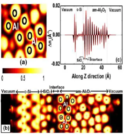
Furthermore Bansall et al. [34] suggest a shift in the ratio between tetrahedrally and octahedrally coordinated Al atoms near the interface due to the formation of aluminum silicate [39]. They support their claim by an electron localized function (ELF) simulation where at the interface there is a decrease in the tetrahedrally coordinated Al atoms and an increase of the average charge on Al atoms indicated by the abundance of O near the interface as depicted in Figure 3.13.
Although charges in our system are usually labeled “fixed charges” some papers report that not all charges are fixed, but some are however mobile. Gielis et al. [40] observed a continuous rise of negative fixed charge during second-harmonic genera-tion (SHG) experiments. This rise in charge is depicted in Figure 3.14a where a laser with an average power of 100 mW is used to induce charge trapping by photons
from Si into Al2O3. After 61 min the laser was shut off for 32 minutes after which
Fig. 3.13.: a) Electron localized function (ELF) of the am-Al2O3structure. (b) ELF of the
c-Si-SiO2-Al2O3 structure indicating the coordination of Al and O atoms. (c)
Electron difference density for interface along the z-direction [34].
was done both before annealing and with a second sample after 425 °C N2 annealing
showing similar behavior to photon induced charge.
These measurements are supported by Liao et al. [41] who also observed an increase
in charge density after illumination of Al2O3 with Air Mass 1.5. Air Mass 1.5 is
similar to direct sunlight under an angle of 42° with the horizon [42]. While these samples were stored in the dark, charge injection partly reverses and the measured charge density reduced towards the initial value [43].
In order for a photon to form additional charge the generated electron can use two
mechanisms to get to the Al2O3−SiO2interface where they are trapped as depicted
in Figure 3.14b:
1. from the valence band of Si into the conduction band of Al2O3 and then
[image:31.595.196.436.65.326.2]sub-sequently diffuse into trap sites located at the SiO2−Al2O3 interface (path 1 in
Figure 3.14b).
2. the electron can either tunnel through the SiO2 layer and then be captured by
trap sites located at the SiO2−Al2O3interface (path 2 in Figure 3.14b)
De-trapping is suspected to take place via recombination of holes and electrons
tunneling through the SiO2 (path 3 in Figure 3.14b).
(a) (b)
Fig. 3.14.: a) Time-dependent SHG intensity for 11 nm Al2O3on Si-100 before annealing
(blue) and after annealing 425 °C N2 (red). A fundamental photon energy
of 1.71 eV, and an average laser power of 100 mW. Between t=60–92 min the laser beam was blocked. The insets show the SHG intensity during the second period of illumination in greater detail. [40] b) Energy band diagram for Si−SiOx−Al2O3interface. The electron trapping and de-trapping transport
4
Simulation
In this chapter the electrostatic model made by using a finite element method (FEM) simulation tool called Comsol Multiphysics 5.1 is discussed. For this simulation the layer stack is build similar to the real device as depicted in Figure 4.1a. Here the substrate layer of silicon is taken as an arbitrary large thickness compared to the
other materials similar to the real sample. For the other layers SiO2, Al2O3 and Pd
their actual thicknesses are used. Fixed charge present at the boundary between
SiO2 and Al2O3 is depicted in black and a ground plate, hence a zero potential is
applied to the bottom of the silicon slab. The red plane represents the location of
the 2DHG at the Si-SiO2interface and is used as a 2D plot plane.
The fixed charge is taken to beQf=−2∗1012cm−2 =−3.2mC m−2 [44]. For all
other parameters the standard values Comsol provides out of the material library are used.
(a) (b)
Fig. 4.1.: a) Layer stack for the finite element method simulation in Comsol Multiphysics, the substrate layer of Silicon is taken as an arbitrary large thickness compared to the other materials similar to the real device. SiO2, Al2O3and Pd represent
actual thicknesses measured for the devices. Fixed charge present at the boundary between SiO2and Al2O3is depicted in purple and a ground plate is added as a
reference at the bottom. The red plane represents the location of the 2DHG at the Si-SiO2interface. b) Isometric representation of the Comsol model build with the
dimensions in nm and gates on top.
Definition of the gate electrodes can be done by hand in Comsol or by importing a .GDS file which is commonly used for layout editing tools such as KLayout. A .GDS layout file from KLayout can be imported via the Geometry import drop down menu in Comsol by selecting the ECAD file (.GDS) as depicted in Figure A.2 in Appendix
A.3. For a 3D simulation setup in Comsol the layer has to become 3D by setting the type of import to ’full 3D’ while additionally its thickness has to be chosen. To ease selection of gates a ’Cumulative Selection 1’ can be created from a single import, without this cumulative selection all boundaries (top,bottom and sides etc.) of the gate have to be selected manually.
The use of the cumulative selection function removes the possibility to apply different gate voltages to different gates out of the same .GDS file. The most suitable solution found so far is to split the gates in multiple .GDS files using the same layer and a second import feature in Comsol. If the import function return an error, removing all excess layers out of the .GDS file might pose a solution.
When the gates are imported a potential of 5 V is applied to all barrier gates and the
electrostatic potential at the red interface, hence Si−SiO2interface can be simulated.
For the simulation an extremely fine mesh is used as depicted in Figure 4.1b resulting in a computational time of three minutes (i7-3630QM @ 2.40 GHz). The ability to be able to change and simulate the effect of different gate designs poses a powerful and versatile tool for further research.
Besides the capability of importing .GDS files, additionally an AFM scan can be imported to get an indication about the actual gate performance of the fabricated device as discussed in Appendix A.3.
Multilayer design is possible but it poses difficulties in correct covering of complex 3D topologies. Besides this, a second layer to accumulate charges is found to be limited by the in real life dielectric layer of devices rather than the layout.
(a) (b)
5
Device layout
In this section the layout of the samples that were fabricated in this thesis will be discussed. It starts with the difference between microscale and nanoscale devices and continues to discuss the way the design iterated during the course of this thesis.
5.1 Microscale device
The macroscale device is used as a starting point for all nanoscale devices with its layout depicted in Figure 5.1. By using this microscale standard design big structures can be patterned with photo-lithography while small nanoscale features connecting to these contact pads can be written with Electron Beam Lithography (EBL). This cooperation of two lithography techniques increases process speed. A total of five bottom/top gates (BG/TG) and four lead gate (LG) contacts pads are available to be used as a break out connection for the nanoscale devices. The starting point for
the EBL lithography can be seen in Figure 5.1b where the p++and n++implanted
regions act as a charge reservoir for holes and electrons.
(a) (b)
Fig. 5.1.: a) Overview of the microscale device fabricated with photo-lithography, the bottom S/D channel p++ doped, and the top S/D n++ doped. b) Zoom in of
the area indicated figure (a) by the dotted lines where the nanoscale device is fabricated by using EBL. The top, bottom and lead gates are depicted as TG, BG and LG respectively.
5.2 Ten gate depletion dot
As a start of the depletion dot topic ten fingered gated nanostructes with a pitch of 70 nm between the barriers and 50 between the plungers are designed. by making use of five top and bottom barriers made from 15 nm of Pd in a single layer as depicted in Figure 5.2a. By tuning the voltages on the barriers, area’s can be depleted allowing for the formation of a dot between two barriers with a third to act as a plunger as depicted in Figure 5.2b. Two lead gates (LG) were incorporated to allow accumulation of holes to the active region of the depletion dot. The small lines indicate single pixel lines and are used with the EBL machine to reach minimal feature size.
(a) (b)
Fig. 5.2.: a) Ten fingered depletion dot design with lead gates to ease hole transport to and from the quantum dot. b) Zoom in of the double quantum dot structure where the outer and middle barriers act as tunnel barriers while the 2nd and 4th barrier act as plungers for the dots. The small lines indicate single pixel lines.
5.3 Ciorga design
(a) (b)
Fig. 5.3.: Single layer Ciorga depletion dot design. a) General layout with gate connections indicated. b) Zoom in on the location of interest with SET indicated in blue and single pixel lines visible as plunger and bottom gate electrode.
5.4 Single hole and single electron dot
As an alternative on the Ciorga design [45] and due to the proof of concept with the ten gated device a double layer device is made to be able to apply charge sensing to the depletion dot by using a SET. This SET will be induced by the second layer lead gate and makes use of the two top barriers. Additionally two bottom barriers and one plunger gate are used to define the depletion hole dot as depicted in Figure 5.4.
(a) (b)
Fig. 5.4.: Two layer depletion dot design with first layer in red with 15 nm palladium gates and second layer 25 nm palladium lead gate. a) General layout with gate connections indicated. b) Zoom in on the location of interest with SET and SHT indicated.
5.4.1 Minimal Design single hole and single electron dot
As a combination the Ciorga design and the previous double layer design are com-bined into a minimal design as depicted in Figure 5.5b. It makes use of a lead gate
to accumulate electrons from the n++regions to the SET where B1 and B3 are used
to define the electron dot. The depletion hole dot is than tuned into place by making use of a combination of all barriers. This device should allow for both transport measurements as well as charge sensing to be able to reach the single or few hole regime.
(a) (b)
6
Experimental methods
The samples in this thesis were fabricated in the MESA+ Nanolab Facility at the University of Twente. The most important steps along with the experimental setup will be discussed.
6.1 Electron beam lithography
Electron beam lithography (EBL) is a technique that uses the beam of a scanning electron microscope with a certain energy, typically 10 to 100 keV for the exposure of resist. The most common positive resist is polymethyl methacrylate, or polymethyl-2-methylpropanoate (PMMA). In positive resists chemical bonds are cracked by the impinging electrons making the exposed region more soluble. In negative resists exposure leads to a strong cross-linking of the molecules and as a result to a lower solubility. The advantage of using an EBL machine is that no mask is required due to the ability to write structures by precise control of the beam. The EBL machine used in the MESA+ cleanroom is the Raith 150-TWO. After exposure the PMMA is developed in an isopropyl alcohol-water (IPA-water) solution of a ratio of 1:10 for one minute or alternatively by using so called cold development.
6.2 Cold development
To reach even smaller feature sizes, higher acceleration voltages, thinner resist and cold development can be used. A higher acceleration voltage leaves a more direct imprint in PMMA due to a decrease in the spread of the backscattered electrons that can overexpose neighboring resist. Additionally a thinner layer of resist will leave a more direct imprint on the sample due to an improvement in aspect ratio. Furthermore, cold development has been shown to improve the EBL resolution and line roughness by using Methyl IsoButyl Ketone (MIBK) with an optimal temperature of approximately -15 °C [46],[47].
A possible downside of using cold development is that development of multiple samples after on another yields different results due to the rapid warm-up of the developer in the cleanroom environment. Secondly if the sample is not properly blow dried afterwards the PMMA starts to overdevelop.
6.3 Metal deposition
The pattern written into PMMA is transfered into metal by evaporation of palladium (Pd) or titanium (Ti). The evaporation of a metal layer is generally done by using the BIOS evaporator were the system is pumped down to vacuum after which a Pd/Ti source is heated with an e-gun to start evaporating. This metal layer is used to define the gates on top of the sample and is usually in the order of tens of nanometers.
6.4 Lift off
After metal has been evaporated, the excess on top of the PMMA is removed by using a lift off procedure. A beaker filled with dimethylsulfoxide (DMSO) as a solvent for the PMMA is placed in an ultrasonic bath and heated to 80 °C. Ultrasonic power can be used moderately to enhance the lift of process when required.
6.5 UV ozone
For the exposure of a device to Ultraviolet (UV) radiation and Ozone (O3) the PR-100
6.6 Experimental setup
In this subsection the experimental setup used for the electrical characterizations of the devices at low temperatures will be discussed in detail.
6.6.1 Measurement preparation
After a sample is taken out of the cleanroom it is glued to the PCB by using PMMA/copolymer and a hotplate at 80 °C for 30 minutes to evaporate solvents. After gluing, the contact pads of the chip are wire bonded to the channels on the PCB allowing for a total of 22 interconnects between the sample and the measurement setup. This is done by using the ultrasonic power of the the wire bonder (WestBond 7476E Wedge-Wedge Wire bonder) to "weld" aluminum wires to both the sample and the PCB. The channels on the PCB can than be connected to the measurement setup and individually addressed by putting the connector into the zero insertion force (ZIF) socket. This PCB can be reused by cleaning it with acetone to dissolve the PMMA after which it is rinsed with IPA and blow dried with a nitrogen gun.
Fig. 6.1.: Custom PCB with 22 break out connections that can be wire bonded to the connections in the ZIF socket. A so called grounding connector shorts all pins to avoid static discharge by keeping them at the same potential. The sample is glued to the PCB by using PMMA.
6.6.2 Dipstick
After the sample has been glued to the PCB it can be loaded into one of the low-temperature setups. Firstly the sample is loaded into the so called "Dipstick" where the PCB is mounted with screws on the end of a long movable rod (Figure 6.2a) after which it is loaded into the liquid helium dewar (Figure 6.2b). The movable rod can be pushed through the lid of the dewar and thereby be lowered into the liquid helium. The benefit of using this setup is that loading and unloading of a sample can
be done within half an hour. The downside is that it goes down to 4.2 K whereas other cryogenic setups are able to reach lower temperatures
Fig. 6.2.: a) Image of the end of the dipstick where the PCB is mounted with screws and connected with the use of a ZIF connector. The temperature sensor below the sample is used to ensure that the sample is immersed into the liquid helium. b) 100 liter liquid helium dewar into which the sample is immersed to let it cool down to a temperature of 4.2 K.
6.6.3 Heliox
For samples that show good characteristics at 4.2 K temperatures can be decreased
even further to decrease the amount of thermal energy (kB T) present in the system
by using the Oxford Heliox Helium3 fridge which is able to go down to 250 mK. A decrease of thermal energy makes electrical transport phenomena more prominent and enables lower currents to be measured due to the decrease of thermal noise in the system. Additionally a vector magnet is present which can be used to apply a magnetic field to measure effects like Zeeman splitting.
6.6.4 Source Measure Unit/ beeper
that it lacks flexibility in applying different potentials to different gates. It is a fast method to get an indication about which devices can be promising.
6.6.5 IV/VI
The connections wire bonded to the PCB are directly connected to the pins on the so called IV/VI rack, as depicted in Figure 6.3. This rack is custom-built at the Delft university and consists of digital to analogue converters (DAC), multiple measure-ment, source and routing modules. The setup is controlled from a computer running QTlab software connected by an optical fiber connection and is battery powered to reduce noise from the power grid. Additionally, current measure, voltage source amplifying and summing modules are used and read out is done by using multi-meter’s connected to the computer via General Purpose Interface Bus (GPIB). The advantage of using the IV/VI rack is that all DACs and thereby hence gates/barriers can be controlled individually and that actual measurements can be done precisely and stored onto the computer.
Fig. 6.3.: IVVI rack with on to the matrix module allowing to individually address each pin and to be able to ground, connect and open them. Below the measurement module connected to the PC by an optical fiber connection, and operated from batteries to prevent noise from the grid.
7
Results
In this chapter the results from the electrical characterization of the fabricated devices are discussed. Based on these results multiple device iterations were made with design specifications as described in the device layout section. Lastly a brief look is taken into manipulation of fixed charge in the system by making use of the UV-ozone photo-reactor, and the possible implementation of titanium gate electrodes is discussed.
It is important to note that the samples were annealed at different temperatures
ranging between 350 and 500◦C in different combinations of gases involving N2, Ar
and H2. Additionally gates are indicated by letters: B indicates a barrier, L indicates
a lead gate and P indicates a plunger. Numbers are added when multiple barriers are in use.
7.1 Ten gate depletion dot
As a proof of concept a double dot design was realized by making use of ten gates
as depicted in Figure 7.1a to deplete the 2DHG at the Si−SiO2 interface [48]. The
lead gates (LG) can be used to accumulate holes to the structure from the highly
doped p++regions by applying a negative voltage.
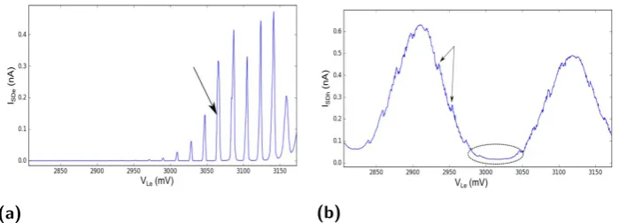
To form a depletion dot, firstly both top and bottom barrier finger gates are used to pinch the source-drain channel. A typical pinch-off curve can be seen in Figure 7.1b for the left top (B3t) and left bottom (B3b) barriers. This measurement is repeated for all top and bottom barrier combinations where the formation of a single dot between B1 and B3 was found to be most optimal with B2 to act as a plunger gate. By parking the plunger gate (B2) on a voltage just before pinch off, one makes sure that the dot is formed between the ends of the top and bottom barrier as depicted in Figure 7.1a (red dots). The barriers (B1 and B3) are swept around their pinch off regime, hence 300-700 mV (B3) and 700-1100 mV (B1) to form a dot as depicted in Figure 7.2a. The formation of a dot is visible by the diagonal lines, and additionally a resonance coupled to B1 can be seen at 1020 mV. By making a top vs. bottom barrier scan it can be seen where this unintentional resonance coupled to B1 is most pronounced. The initial sweep ratio of B1t and B1b is indicated by the blue line in Figure 7.3a and is moved around the defect by applying an offset of 150 mV to
(a)
(b)
Fig. 7.1.: a) Typical AFM image of the ten gated depletion dot design with 15 nm palladium gates. Here B1,B2,B3,B4 and B5 indicate the barriers where a ’t’ or ’b’ is added to indicate top and bottom barriers respectively. L indicates the lead gate. b) Pinch off graph for B3. Resonances around pinch off at 600 mV could be due to the formation of an unintentional dot between both barriers or a defect in the lattice.
HereVSD= 1mV,B2 =B3 =B4 =B5 = 0mV.
[image:46.595.99.438.73.239.2]B1t as indicated by the red line. Additionally this shift can be visualized with a simulation of the electrostatic field where the blue dot represents the defect and black lines are used as a guide to the eye to indicate the shift in field as depicted in Figure 7.3b. A defect can be a dangling bond, lattice defect or interstitial, and can be decoupled as indicated in Figure 7.2b where the dot behavior is less because gate space was not optimized and a low resolution scan is made.
The lead gate incorporated into this design turned out to be not required for the formation of a depletion dot indicating that a proper 2DHG is present in the system and no additional bias is required to accumulate holes.
(a) (b)
Fig. 7.2.: a) Quantum dot formed between B1 and B3 indicated by the diagonal lines. A resonance coupled to B1 can be seen around 1020 mV.Here VSD = 0.4 mV,
(a)
(b)
Fig. 7.3.: a) B1b vs. B1t scan with in blue the original B1t and B1b scan ratio, and depicted in red the adjusted ratio to tune around the defect. HereVSD= 0.4mV,
B2 =B3 =B4 =B5 =−200mV.b) Color plot of the electric potential (V) in a Comsol simulation with a defect indicated as a blue dot, and black guides to the eye to indicate tuning around a defect.
7.2 Electron accumulation and hole depletion dot
As discussed in the theory section, charge sensing is a powerful tool for measuring down to the few or even single hole regime. For this purpose a double layer device is fabricated with a second layer lead gate to accumulate electrons for the single-electron dot between both top barriers to act as a sensor dot, recall Figure 5.4b. For the depletion dot an additional set of bottom barriers in incorporated, and a plunger gate is used to tune the electrochemical potential of the depletion dot without changing the tunnel barriers.
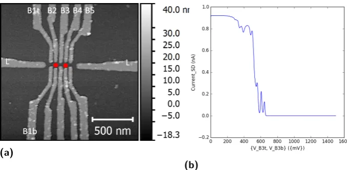
A typical AFM image of the first write test is depicted in Figure 7.4a where it can be seen that the bottom center barrier is a bit wider than the other two due to proximity effect of the EBL. Furthermore the two fingers at the top are slightly close to one another, leaving a small region available for the SET.
Firstly an electron dot is defined by accumulating electrons from the n++ regions
by using the lead gate with approximately 3.0 V, and the two top barrier gates (e_B1 and e_B2). An approximate 1.4 V is required for the electron barriers at 3.0 V lead gate voltage which lowers when the lead voltage increases as also clear from the oscillations to the lead vs. barrier scan in Figure 7.4d. This indicates that the lead gate can be used to tune the barrier voltages in correspondence with both the electron and hole dot simultaneously. A main requirement is a good dielectric between the first and second layer to allow high voltages on the lead gate without leakage.
After defining the SET, secondly a hole dot is formed with initial starting conditions as indicated by the black dot as depicted in Figure 7.4c. The performance of this device was however limited since h_B1 was broken, so a depletion dot without a
plunger is formed between h_B2 and h_P as depicted in Figure 7.4b. Resonances of a performance limited intentional dot can be seen devoted to both the design, small region for the SET and the formation of the depletion dot with the plunger gate as a barrier.
Due to the limited performance of both dots charge sensing is not implemented and device iteration continues. It is however demonstrated that an electron accumulation and hole depletion can be formed simultaneously in gate space within the same device.
(a) (b)
(c) (d)
Fig. 7.4.: a) AFM image of the first and second layer with voltages to indicate the operating regime and barriers indicated.
b) Hole dot formed with electron leads at the parking spot at the black dot in (c). Here VSD = 0.4 mV, e_B1 = 1440 mV, e_B2 = 1410 mV, L = 3650 mV,
h_B1 =−500mV.
c) Electron dot formed between e_B1 and e_B2. The red line indicates the ratio e_B1 and e_B2 for the scan in (d) and the black dot shows the parking spot for the scan in Figure (b).HereVSD= 0.4mV,h_B1 = 0mV,h_B2 = 0mV,h_P = 0
mV,L= 3650mV.
d) Lead vs. e_B1&e_B2 scan where the most optimal location for the lead can be found by looking at the resonance peaks. HereVSD= 0.4mV,h_B1 = 0mV,
7.3 Ciorga design
As it turned out from the first two generation of devices a slightly different approach might improve the behavior of the depletion dot, after which charge sensing could be implemented into the design. As an advantage only a single layer device has to be fabricated to define a depletion dot allowing faster fabrication and thereby device iterations. A design proven to be capable of reaching the single-electron regime in a GaAs structure was adapted from Ciorga et al. [45]. The main difference is that Ciorga used a GaAs stack which has a lower effective mass allowing for a bigger spacing between energy states making them easier to probe.
A typical AFM scan of the Ciorga design is depicted in Figure 7.5a where the colored dots can be ignored for the moment. The formation of a quantum dot by the Ciorga design made from palladium can be seen in Figure 7.6a where clear resonances cou-pled equally to both barrier B1 and B3 are visible as depicted by the black line. On top of the intentional quantum dot the behavior of two unintentional dots coupled each to one of the barriers can be seen as indicated by the red and white lines.
(a) (b)
Fig. 7.5.: a) AFM scan after metal lift off with in red the intentional dot and in blue two unintentional dots depicted, and gates indicated. b) Comsol simulation with the Ciorga gate design as shown in (a) and the color-plot indicating the amount of fixed charge at the 2DHG layer noted in electric potential (V). The shape of the gate electrodes is indicated in green.
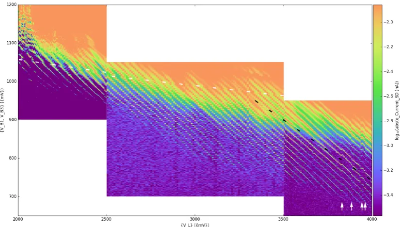
The capacitive coupling of these unintentional dots to the barriers can be extracted to get a quantitative indication of the location of these dots. For this, the constant interaction model is hold valid with Equation 3.15 and 3.16 to describe mutual capacitances between the barriers.
When extracted out of the B1 vs. B3 scan: Cg1/Cg3=2.74 indicating that dot 1
couples 2.74 times stronger to B1 than B3, and vise versa for dot 3: Cg3/Cg1= 2.92
with B2=1100 mV. By changing the potential on B2 the tunnel barriers move in the 2DHG and thereby the location of the unintentional dots coupled to B1 and B3. With B2=3000 mV the dots tend to move further from B2 and closer to B1
and B3 as indicated by the coupling ratio’s being respectively: Cg1/Cg3=6.36 and
Cg3/Cg1 = 6.43, thereby shifting them a factor of 2.8 closer to the big barriers. It is
noted from these numbers that coupling to both gates is highly symmetrical which can be explained due to the well defined symmetrical gate structures. To see whether these unintentional dots form in complete gate space or between two barriers, a B3 vs. B2 scan is made as depicted in Figure 7.7. From this no optimal position for both barriers could be found since unintentional resonances stays present as more clear in the close-up. The expected location of both the intentional and unintentional dots are depicted in the AFM scan in Figure 7.5a as red and blue dots respectively.
(a) (b)
Fig. 7.6.: a) B1 vs. B3 plot where the formation of the intentional quantum dot can be seen by the diagonal lines indicated by the blue line with on top unintentional quantum dots forming coupled unequally to B1 and B3 as indicated by the red and white lines.HereVSD= 0.4mV,B2 = 1100mV,P= 4000mV.b) B1&B3 vs. P
plot in which it can be seen that the dot couples weakly to the plunger compared to the barriers.HereVSD= 0.4mV,B2 = 2250mV.
In Figure 7.8 it can be seen that the coupling between the plunger and B1 and B3 is a factor of 24, indicating that the plunger is lowly coupled to the dot and the barriers highly. This can be explained by the fact that the plunger is relatively small and far away from the dot as compared to the barriers B1 and B3.