N A N O E X P R E S S
Open Access
Impacts of Annealing Conditions on the
Flat Band Voltage of Alternate La
2
O
3
/Al
2
O
3
Multilayer Stack Structures
Xing-Yao Feng, Hong-Xia Liu
*, Xing Wang, Lu Zhao, Chen-Xi Fei and He-Lei Liu
Abstract
The mechanism of flat band voltage (VFB) shift for alternate La2O3/Al2O3multilayer stack structures in different
annealing condition is investigated. The samples were prepared for alternate multilayer structures, which were annealed in different conditions. The capacitance-voltage (C-V) measuring results indicate that the VFBof samples
shift negatively for thinner bottom Al2O3layer, increasing annealing temperature or longer annealing duration.
Simultaneously, the diffusion of high-k material to interfaces in different multilayer structures and annealing conditions is observed by X-ray photoelectron spectroscopy (XPS). Based on the dipole theory, a correlation between the diffusion effect of La towards bottom Al2O3/Si interface and VFB shift is found. Without changing
the dielectric constant k of films, VFB shift can be manipulated by controlling the single-layer cycles and annealing
conditions of alternate high-kmultilayer stack.
Keywords:Flat band voltage, La2O3/Al2O3multilayer, Dipoles, Diffusion effect, Interface layer
Background
High dielectric constant (high-k) materials have been extensively used to substitute conventional SiO2gate
ox-ides for its prominent properties such as small equiva-lent oxide thickness (EOT) and low leakage current. During the past years, researchers have paid lots of attentions to high-k materials, such as hafnium oxide (HfO2), yttrium oxide (Y2O3), zirconium oxides (ZrO2),
lanthanum oxide (La2O3), aluminum oxide (Al2O3), and
other transition-metal oxides. Among them, La2O3 is
considered a remarkable candidate because of its high dielectric constant (approximately 25) and large band gap (approximately 5.8 eV). However, the application of high-k materials also cause lots of new problems and challenges [1, 2]. Recently, the properties of La2O3and
Al2O3gate stacks have been studied by many researchers,
and much promotion has been made in restraining leak-age current and suppressing the formation of parasitic interface [3–5].
Furthermore, flat band voltage has been regarded as one of the most critical parameters for the design and
fabrication of semiconductor devices. Earlier researchers claimed that the fixed charges are the main factor for flat band voltage (VFB) shift [6]. However, Dr. Wang pointed
out there was no correlation between VFB and fixed
charges because the film HfxLa1−xOykeep the same VFB
for different film thicknesses [7, 8]. Researchers also re-vealed that the main origin of VFBis the dipoles between
high-k/interface layer [9, 10]. Besides, the atomic mech-anism of VFBshifts for different high-kgate stacks is also
discussed specifically by Lin and Robertson [11, 12]. However, the influence of the film structure and anneal-ing conditions on VFBhas not been fully investigated. In
this study, firstly, a model of VFBincluding the interfaces
of metal/high-k and high-k/Si was introduced. Then, alternate La2O3/Al2O3 multilayer stacks were prepared
with different single-layer cycles by atomic layer depos-ition (ALD) and annealed in different temperatures and duration. The electrical and physical characteristics of the samples were investigated. Based on the theory of dipoles and diffusion effect, the mechanism of VFB shift
was studied.
* Correspondence:[email protected]
Key Laboratory for Wide-Band Gap Semiconductor Materials and Devices of Education, School of Microelectronics, Xidian University, Xi’an 710071, China
Methods
Firstly, p-type Si(100) wafers were washed in deionized water and chemically etched with diluted HF for 3 min to remove the native oxide. Then, alternate La2O3/Al2O3
multilayer high-k stacks with different single-layer cycles were deposited on Si wafers by ALD reactor (Picosun R-150, Espoo, Finland) in 300 °C. La(i-PrCp)3and
trinethylu-minium (TMA) were used as precursors of La and Al, respectively. Besides, O3 was used as oxidant, and
ultra-high purity nitrogen (N2, 99.999 %) was employed as carrier
and purge gas. After deposition, the rapid thermal anneal-ing (RTA) process was carried out at different temperatures for different duration in N2ambient. For further analysis,
annealed La2O3/Al2O3film thickness (without metal gate)
was examined by Woollam M2000D (Woollam Co. Inc., Lincoln, NE, USA) spectroscopic ellipsometry (SE). X-ray photoelectron spectroscopy (XPS) was used to examine the bonding structures and chemical quantitative composition of the films. C1s peak from adventitious carbon at 284.6 eV [13] was used as an internal energy reference during the analysis. Besides, 100-nm-thick Al was deposited by magne-tron sputtering as electrode, and then, capacitance-voltage (C-V) measurement was carried out using Agilent B1500A semiconductor analyzer at the frequency of 100 kHz.
Results and Discussion
Taking into consideration of fixed charges and interfacial dipoles, the VFBof conventional metal/SiO2/Si metal oxide
semiconductor (MOS) structure can be expressed as [14]:
VFB ¼φms
q −EOT
Q0
ε0εox
þ Δmetal=SiO2þΔSiO2=Si
;
ð1Þ
whereφmsis the work function difference between metal and Si substrate and Q0 represents the fixed charges
located in oxide layer.Δmetal/SiO2andΔSiO2/Si are di-poles located in the interface of metal/SiO2and SiO2/Si.
In this work, SiO2 is substituted by high-k materials
Al2O3 and La2O3, so the VFB of samples with alternate
high-kdielectric gate stacks can be expressed as:
VFB ¼φms
q −d0
Q0
ε0εAl2O3
−d1 ε Q1 0εLa2O3
þ Δmetal=high‐kþΔhigh‐k=SiþΔLa2O3=Al2O3
: ð2Þ
In this equation,Q0andQ1represent the fixed charges
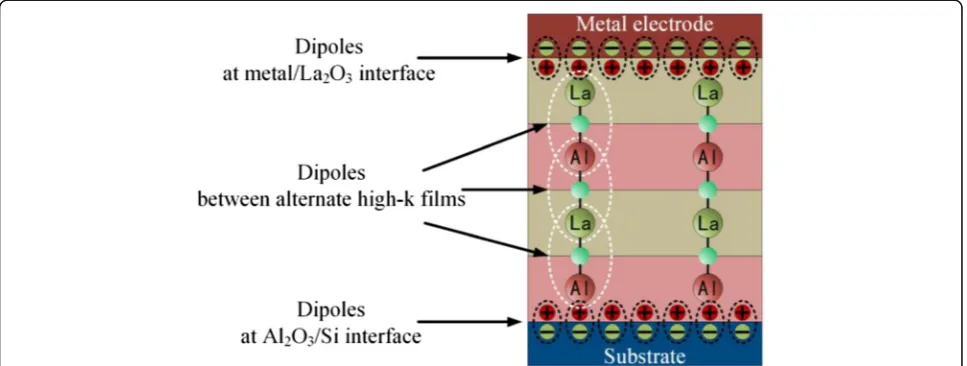
in Al2O3 and La2O3 films, respectively. As shown in
Fig. 1, all dipoles can be separated into three kinds. They are the dipoles between the alternate high-k films, the dipoles at interfaces of metal/La2O3, and dipoles at
inter-faces of Al2O3/Si. Between the alternate high-k layers,
the dipoles La–O–Al and Al–O–La have reverse sequence which can cancel out each other. So these dipoles do not create net dipole.
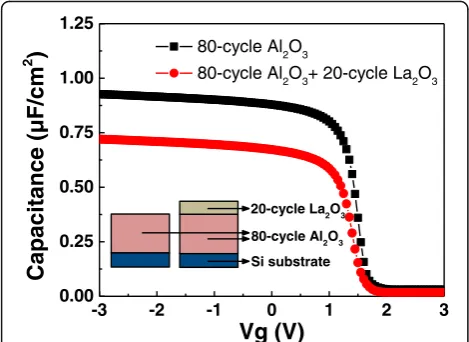
Furthermore, some researches have proved that the contribution of dipoles at metal/high-k interface to the VFB shift can be neglected [10, 15, 16]. For inspecting
this point of view, two samples were prepared with dif-ferent high-k films, and then, the RTA process was carried out at 600 °C for 60 s in N2 atmosphere. Their
simplified schematic structures and C-V curves are shown in Fig. 2. It should be noted that the two films show approximately the same VFB: 1.49 V (without
La2O3 inserted layer) and 1.47 V (with La2O3 inserted
layer). The insensitiveness of VFB values to the kind of
dipoles at metal/high-k interface clearly indicates the metal/high-k interface is not one of the origin of VFB
shift. Therefore, in this work, the fixed charges Q0and
Q1 and the dipoles at interface of Al2O3/Si need to be
examined on the next step.
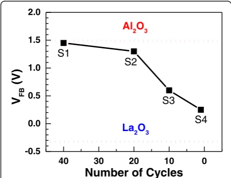
[image:2.595.57.541.529.712.2]Samples S1~S5 were deposited for different structures in an identical annealing condition (annealed at 600 °C for 60 s in N2 atmosphere). The schematic of alternate
high-k films S1~S5 is shown in Fig. 3. For each of the samples S1~S4, 40-cycle La2O3and 40-cycle Al2O3were
deposited with different single-layer cycles (from S1 to S4 are 40, 20, 10, and 1 cycle of single layer). In order to investigate the influence of fixed charges on VFB, as
shown in Fig. 3b, e, the sample S5 was deposited with the same single-layer cycles but double number of layers as S2. The structures and thicknesses of samples S1~S5 are listed in Table 1.
Figures 4 and 5 show the C-V curves and VFB shifts of
samples S1~S5. Samples S1~S4 have very close accumu-lation capacitance. The EOTs of samples S1~S5 are extracted by NCSU CVC program [17], which are 2.21, 2.20, 2.21, 2.29, and 4.16 nm, respectively. The dielectric constants are 12.46, 12.44, 12.34, 12.89, and 12.56, re-spectively. The VFB of samples S1~S5 are 1.45, 1.30,
0.60, 0.25, and 1.30 V, respectively. For 80-cycle pure Al2O3 and 80-cycle pure La2O3 films deposited and
annealed in the same condition with S1~S5, VFBare 1.49
and −0.32 V, which is shown in Fig. 5. We notice that VFBbecome smaller shifting from the VFB of pure Al2O3
film to the pure La2O3 direction for a thinner single
layer (from 40 to 1 cycle). In a recent report [10], a negative VFB shift is observed for a thicker La2O3
inserted layer at HfO2/Si interface which comes to a
similar conclusion with our work. Furthermore, VFB is
the same for samples S2 and S5, which indicates the Al2O3 and La2O3 films have few fixed charges.
There-fore, the fixed charge Q0 and Q1 in Eq. 2 can be
neglected for studying VFB shift. As discussed, the VFB
shifts of S1~S4 have no relevance to the dipoles between alternate high-klayers and dipoles at metal/high-k inter-face. Therefore, it is clear that such a shift (from 1.45 to 0.25 V) is supposed to be relevant to the variation of dipoles at Al2O3/Si interface.
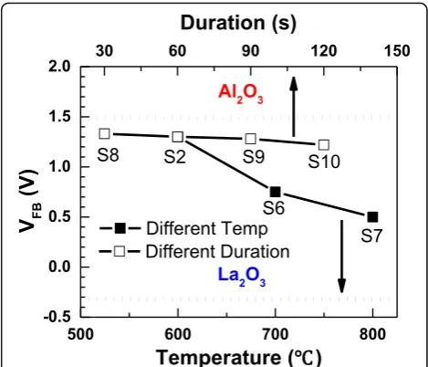
For further investigation about the mechanism of VFB
shift for high-k gate stacks, different annealing condi-tions were employed after the ALD deposition. As shown in Table 2, samples S2 and S6~S10 were depos-ited for identical structure and then annealed at different temperatures (600, 700, and 800 °C) for different dur-ation (30, 60, 90, and 120 s) in N2atmosphere. The
cor-relations between C-V curves and annealing conditions of samples S2 and S6~S10 are shown in Fig. 6. The EOTs of samples S2 and S6~S10 extracted by NCSU CVC program [17] are 2.20, 2.23, 2.29, 2.20, 2.20, and 2.20 nm, respectively, and the dielectric constant k can be figured out as 12.44, 12.61, 12.26, 12.55, 12.53, and 12.62, respectively. As shown in Fig. 7, the VFB of
sam-ples S2 and S6~S10 are 1.3, 0.75, 0.5, 1.33, 1.28, and 1.22 V, respectively, which have a remarkable negative shift with increasing annealing temperature and a slight negative shift with increasing duration. Similar trend of VFB shift (approximately 1 to 0.6 V) was also reported
for HfO2 and Al2O3 stacks at different annealing
temperature (400 and 1000 °C, respectively) [9].
Then, XPS was employed to examine the variation of bonding structure. Figure 8 shows the O1s XPS spectra of annealed samples S1~S4, and each of the spectra was fitted with four peaks Si–O–Al (532.5 eV), Al–O–Al (531.5 eV), Al–O–La (530.9 eV), and La–O–La (528.75 eV). It is found that La–O–Al peaks become lar-ger while Al–O–Al and La–O–La peaks become smaller from S1 to S4. That is attributed to more La2O3/Al2O3
[image:3.595.56.291.88.259.2]interface layers formed with decreasing single-layer cy-cles. As we discussed above, the dipoles La–O–Al and Al–O–La can cancel each other, so the variation of these peaks makes no contribution to VFBshift.
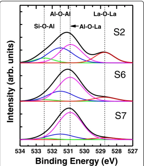
Figure 9 show the O1s XPS spectra of samples S2, S6, and S7. More Al–O–La bonds and less Al–O–Al and La–O–La bonds are observed from S2 to S7, which indi-cates more Al2O3and La2O3diffuse into each other and
form LaAlO3at Al2O3/La2O3interface at higher
anneal-ing temperature. The value of diffusion coefficient mainly depends on the kinds of diffusion substance and diffusion medium as well as the diffusion temperature.
-3 -2 -1 0 1 2 3
0.00 0.25 0.50 0.75 1.00 1.25
20-cycle La2O3
Capacitance (µF/cm
2
)
Vg (V)
80-cycle Al2O380-cycle Al2O3+ 20-cycle La2O3
80-cycle Al2O3
Si substrate
Fig. 2The simplified schematic structures and C-V curves of La2O3/
Si and Al2O3/La2O3/Si
Table 1The structures and thicknesses of annealed samples S1~S5
Sample Film structures Thickness (nm) S1 1 × (40-cycle Al2O3+ 40-cycle La2O3) 7.06
S2 2 × (20-cycle Al2O3+ 20-cycle La2O3) 7.02
S3 4 × (10-cycle Al2O3+ 10-cycle La2O3) 6.99
S4 40 × (1-cycle Al2O3+ 1-cycle La2O3) 7.57
S5 4 × (20-cycle Al2O3+ 20-cycle La2O3) 13.4
[image:3.595.56.291.639.724.2]So this trend is due to the larger diffusion coefficient obtained at higher temperature.
In both Figs. 8 and 9, we notice that there is only small amount of Si–O–Al bonds which show a slight decrease for thinner single layer or higher annealing temperature. Thinner single layer means a thinner bottom Al2O3
layer, which leads to more La2O3diffusing into Al2O3/Si
interface and replacing the Si–O–Al with Si–O–La bonds. Based on the theory of diffusion, more La2O3can
diffuse through the bottom Al2O3layer forming Si–O–
La bonds at higher annealing temperature. Similarly, in-creasing annealing duration can also cause more La2O3
diffusing into Al2O3/Si interface. That is why, the
amount of Si–O–Al bonds declines. This diffusion effect of high-kmaterial after annealing process is also proved in report [9], which shows HfO2and Al2O3stacks
diffus-ing into each other and into the metal/high-kand
high-k/Si interfaces after annealing process at different temperatures.
On the other hand, Si–O–Al and Si–O–La bonds are located at the interface of high-k/Si. According to the dipole theory discussed above, this substitution of La for Al should be responsible for the negative VFB shift.
Therefore, we should also discuss how the increasing La–O–Si bonds at Al2O3/Si interface influences the VFB.
La has weaker electronegativity than Al (La ~ 1.11, Al ~ 1.61). When Al is substituted by La, compared with Al, electrons will be further from La and move towards O. So the dipole La–O presents a larger polarity compared with dipole Al–O. It means a larger electrostatic poten-tial, which can increase the band offset and finally cause the VFB shift. It is concluded that the more Al is
substituted by La at Al2O3/Si interface the closer to blue
dotted line, the VFB will be. Moreover, the VFB shift in
Fig. 3The schematic structures of samples S1~S5
-3 -2 -1 0 1 2 3
0.00 0.25 0.50 0.75 1.00 1.25
20 cycles single layer
1 cycle single layer
10 cycles single layer 20 cycles single layer
40 cycles single layer
Capacitance (µF/cm
2
)
Vg (V)
S1 S2 S3 S4 S5
Fig. 4C-V curves of samples S1~S5 which contain 40, 20, 10, 1, and 20 single-layer cycles, respectively
40 30 20 10 0
-0.5 0.0 0.5 1.0 1.5 2.0
La2O3 S4
S3 S2
V
FB(V)
Number of Cycles
S1
Al2O3
Fig. 5VFBof samples S1~S5. Theredandblue dotted linesrepresent
[image:4.595.59.540.87.273.2] [image:4.595.304.538.522.702.2] [image:4.595.57.291.531.703.2]different annealing temperatures is much bigger com-pared with different duration. It can be explained by the exponential relationship between the temperature and diffusion coefficient. Therefore, a feasible way to modulate the VFB of alternate high-k multilayer stack
gate is to control the single-layer cycles and annealing conditions.
In addition, we should notice that the diffusion should be bidirectional, meaning the Al2O3should also diffuse
into the metal/La2O3 interface. But the experiment in
our work shows no relevance between the metal/high-k interface and the VFB shift. In fact, some researchers
hold the contrary opinions to our work by investigating the high-kinserted layer at metal/high-kinterface. How-ever, in these reports [18, 19], the high temperature annealing (1000 °C) and thin high-kfilms (approximately 4 nm) may lead to the non-negligible diffusion of inserted layer material to the high-k/Si interface and re-sult in VFB shift. Furthermore, the reason that dipoles at
metal/high-k and high-k/Si interface present distinct effect on VFBshift is supposed to be relevant to the
dif-ferent properties of bonds. Unlike La–O–Si or Al–O–Si,
[image:5.595.304.539.87.288.2]the bonds between metal gate and high-k material are ionic bonding (La–O–Al or Al–O–Al), which may result in distinctly different electrical properties of dipoles. However, further work is still underway towards a more specific explanation about that.
Table 2The annealing conditions and thicknesses of samples S2 and S6~S10
Sample Temperature (°C) Duration (s) Thickness (nm)
S2 600 60 7.02
S6 700 60 7.21
S7 800 60 7.20
S8 600 30 7.08
S9 600 90 7.07
S10 600 120 7.12
Samples S6~S10 have the same film structure with S2: 2 × (20-cycle Al2O3+ 20-cycle La2O3)
Fig. 6C-V curves of samples S2 and S6~S10. Samples S2, S6, and S7 were annealed at different temperatures for 60 s, while samples S2 and S8~S10 were annealed at 600 °C for different duration
Fig. 7VFBof samples S2 and S6~S10. S2 is a shared point for
different annealing temperature and duration. Theredandblue dotted linesrepresent the VFBof 80-cycle Al2O3 and La2O3
films, respectively
534 533 532 531 530 529 528 527
S4
S3
S2
Al-O-LaLa-O-La Al-O-Al
Intensity (a
rb. units)
Binding Energy (eV)
Si-O-AlS1
[image:5.595.56.291.110.208.2] [image:5.595.306.540.434.707.2] [image:5.595.56.292.522.693.2]Conclusions
The C-V curves and XPS results of alternate La2O3/
Al2O3 multilayer stacks are investigated in the paper.
It is concluded that the main factor of VFB shift is
the dipoles at high-k/Si interface. Furthermore, the VFB of samples shifts negatively and varies from the
VFB of pure Al2O3 to the pure La2O3 direction for
thinner bottom Al2O3 layer, increasing annealing
temperature or longer annealing duration. In such a condition, more La2O3 can diffuse into the Al2O3/Si
interface and form La–O–Si bonds. Because of a weaker electronegativity of La, dipole La–O has stronger polarity than dipole Al–O. It leads to the band offset and negative VFB shift. As a result, a
feasible way to modulate VFB without changing the
dielectric constant kof films is proposed.
Abbreviations
ALD:Atomic layer deposition; C-V: Capacitance-voltage; EOT: Equivalent gate oxide thickness; MOS: Metal oxide semiconductor; RTA: Rapid thermal annealing; SE: Spectroscopic ellipsometry; TMA: Trinethyluminium; VFB: Flat band
voltage; XPS: X-ray photoelectron spectroscopy
Acknowledgements
This research is supported by the National Natural Science Foundation of China (Grant Nos. 61376099 and 61434007) and the Foundation for Fundamental Research of China (Grant No. JSZL2016110B003).
Authors’contributions
XyF generated the research idea, analyzed the data, and wrote the paper. XyF and XW carried out the experiments and the measurements. XW, LZ, CxF, and HlL participated in the discussions. HxL has given the final approval of the version to be published. All authors read and approved the final manuscript.
Authors’information
XyF and HlL are Master students in the Xidian University. HxL is a professor in the Xidian University. XW, LZ, and CxF are PhD students in the Xidian University.
Competing interests
The authors declare that they have no competing interests.
Received: 8 July 2016 Accepted: 7 September 2016
References
1. Zhao Y, Kita K, Kyuno K et al (2009) Band gap enhancement and electrical properties of La2O3films doped with Y2O3as high-k gate insulators.
Appl Phys Lett 94:042901
2. Cao D, Cheng X, Yu Y et al (2013) Competitive Si and La effect in HfO2phase stabilization in multi-layer (La2O3)0.08(HfO2) films.
Appl Phys Lett 103:081607
3. Wang X, Liu HX, Fei CX et al (2015) Silicon diffusion control in atomic-layer-deposited Al2O3/La2O3/Al2O3gate stacks using an Al2O3barrier layer.
Nanoscale Res Lett 10:1–6
4. Lee WJ, Ma JW, Bae JM et al (2013) The diffusion of silicon atoms in stack structures of La2O3and Al2O3. Curr Appl Phys 13:633–639
5. Kim Y, Woo S, Kim H et al (2010) Effects of an Al2O3capping layer on
La2O3deposited by remote plasma atomic layer deposition. J Mater Res 25:
1898–1903
6. Lee JH, Koh K, Lee NI et al (2000) Effect of polysilicon gate on the flatband voltage shift and mobility degradation for ALD-Al2O3gate dielectric. In:
International Electron Devices Meeting., pp 645–648
7. Wang XP, Li MF, Ren C et al (2006) Tuning effective metal gate work function by a novel gate dielectric HfLaO for nMOSFETs. IEEE Electron Device Lett 27:31–33
8. Wang XP, Lim EJ, Yu HY et al (2007) Work function tunability of refractory metal nitrides by lanthanum or aluminum doping for advanced CMOS devices. IEEE Transact Electron Devices 54:2871–2877
9. Kornblum L, Meyler B, Cytermann C et al (2012) Investigation of the band offsets caused by thin Al2O3layers in HfO2based Si metal oxide
semiconductor devices. Appl Phys Lett 100:062907
10. Kakushima K, Okamoto K, Adachi M et al (2008) Origin of flat band voltage shift in HfO2gate dielectric with La2O3insertion. Solid-State Electr 52:1280–1284
11. Lin L, Robertson J (2009) Atomic mechanism of flat-band voltage shifts by La2O3and Al2O3in gate stacks. Appl Phys Lett 95:012906
12. Lin L, Robertson J (2009) Atomic mechanism of flat-band voltage shifts at La2O3, Al2O3and Nb2O5capping layers. Microelectr Eng 86:1743–1746
13. Pelloquin S, Saint-Girons G, Baboux N et al (2013) LaAlO3/Si capacitors:
comparison of different molecular beam deposition conditions and their impact on electrical properties. J Appl Phys 113:034106
14. Kaushik VS, O'Sullivan BJ, Pourtois G et al (2006) Estimation of fixed charge densities in hafnium-silicate gate dielectrics. IEEE Transact Electron Devices 53:2627–2633
15. Yamamoto Y, Kita K, Kyuno K et al (2007) Study of La-induced flat band voltage shift in metal/HfLaOx/SiO2/Si capacitors. Japanese J Appl Phys 46:
7251–7255
16. Iwamoto K, Kamimuta Y, Ogawa A et al (2008) Experimental evidence for the flatband voltage shift of high-k metal-oxide-semiconductor devices due to the dipole formation at the high-k/SiO2interface. Appl Phys Lett
92:132907
17. Hauser J (2000) NCSU CVC software, version 7.0. Raleigh, USA: Department of Electrical and Computer Engineering, North Carolina State University 18. Pantisano L, Schram T, Osullivan B et al (2006) Effective work function modulation
by controlled dielectric monolayer deposition. Appl Phys Lett 89:113505 19. Narayanan V, Paruchuri V, Bojarczuk N et al (2006) Band-edge high-performance
high-k/metal gate n-MOSFETs using cap layers containing group IIA and IIIB elements with gate-first processing for 45 nm and beyond. In: VLSI Technology., pp 178–179
534 533 532 531 530 529 528 527
S7
S6
Intens
ity
(a
rb. units)
Binding Energy (eV)
Si-O-AlAl-O-Al
Al-O-La La-O-La