NAN O R EVIE W
Open Access
Status and Prospects of ZnO-Based
Resistive Switching Memory Devices
Firman Mangasa Simanjuntak
1, Debashis Panda
2, Kung-Hwa Wei
1and Tseung-Yuen Tseng
3*Abstract
In the advancement of the semiconductor device technology, ZnO could be a prospective alternative than the
other metal oxides for its versatility and huge applications in different aspects. In this review, a thorough overview
on ZnO for the application of resistive switching memory (RRAM) devices has been conducted. Various efforts that
have been made to investigate and modulate the switching characteristics of ZnO-based switching memory devices
are discussed. The use of ZnO layer in different structure, the different types of filament formation, and the different
types of switching including complementary switching are reported. By considering the huge interest of transparent
devices, this review gives the concrete overview of the present status and prospects of transparent RRAM devices
based on ZnO. ZnO-based RRAM can be used for flexible memory devices, which is also covered here. Another
challenge in ZnO-based RRAM is that the realization of ultra-thin and low power devices. Nevertheless, ZnO not
only offers decent memory properties but also has a unique potential to be used as multifunctional nonvolatile
memory devices. The impact of electrode materials, metal doping, stack structures, transparency, and flexibility on
resistive switching properties and switching parameters of ZnO-based resistive switching memory devices are
briefly compared. This review also covers the different nanostructured-based emerging resistive switching memory
devices for low power scalable devices. It may give a valuable insight on developing ZnO-based RRAM and also should
encourage researchers to overcome the challenges.
Keywords:
Resistive switching, Resistive memory, RRAM, Memristor, ZnO, Nonvolatile memory
Review
Introduction
Semiconductor memory is an indispensable component
and backbone of all modern electronic devices. All
recognizable computing platforms ranging from
hand-held devices to large super-computer storage systems
are used for storing data, either temporarily or
perman-ently, as per their requirement [1]. Based on storing data
volatility, memories are basically classified into two
cat-egories, (i) volatile memory and (ii) nonvolatile memory.
In a volatile memory, the stored data is lost immediately
after the power is turned off whereas nonvolatile
mem-ory (NVM) is capable to retain the stored data for a long
time even after the power is off. Demands on NVMs are
increasing extensively, due to the huge popularity of
consumer electronics and portable gadgets, such as
smart phone, memory card, and USB storage devices,
where NVM is one of the basic component [2–5].
Over the last few decades, a variety of NVM devices
such as flash memory, resistive random access memory
(RRAM), phase change memory (PCM), ferroelectric
memory (FeRAM), and magnetic random access
mem-ory (MRAM) have emerged, though each has some
tech-nical limits, such as scalability, retention, switching
power, and reliability aspects [2, 5–33]. Among them,
resistive switching memory devices are expected to be
one of the promising candidates for future nanoscale
memories [34–46].
RRAM Technology
In 1971 [47, 48], memristor (memory-resistor), later also
called as resistive switching memory [31, 32], is firstly
introduced and theorized as the fourth classical circuit
elements by Chua. The element was realized in the form
of active circuit which then behaves like a nonlinear
resistor with memory [47]. A few years before the
* Correspondence:[email protected]3
Department of Electronics Engineering and Institute of Electronics, National Chiao Tung University, Hsinchu 30010, Taiwan
Full list of author information is available at the end of the article
© 2016 The Author(s).Open AccessThis article is distributed under the terms of the Creative Commons Attribution 4.0 International License (http://creativecommons.org/licenses/by/4.0/), which permits unrestricted use, distribution, and reproduction in any medium, provided you give appropriate credit to the original author(s) and the source, provide a link to the Creative Commons license, and indicate if changes were made.
introduction of the new element, nonlinear resistance
changes had been observed in various metal oxides [49].
Gibbons and Beadle, in 1964 [50], proposed the
exist-ence of conducting filament (CF) to control the
resist-ance changes in Ag/NiO/Ni device. However, the origin
of such conduction is not explored until Simmons and
Verderber in 1967 [51] suggested that the conduction of
reversible switching in Au/SiO/Al device was originated
from the conduction electrons travel by tunnelling
be-tween sites provided by Au ions injected from Au
elec-trode. These findings may lead to the development of
RRAM applications. Nowadays, the role of CF is
acknowledged to be as a
“circuit breaker”
that determine
the principle of the switching itself [37]. Much efforts
has been conducted to modulate its shape, size, and
number and to understand the mechanism that define
the switching behavior [52–56].
Advantages of ZnO for RRAM Applications
Resistive random access memory have been developed
in various structures, such as sandwich [52–56], planar [57,
58], laterally bridge [59], single nanorod/nanowire [60–75],
nanobelt [76], and nanoisland [77, 78]. Nevertheless, the
basic RRAM structure should consist of two opposite
elec-trodes and a storage material, as depicted in Fig. 1. Organic
[79], inorganic [44,] or hybrid [80] insulating materials can
be used as a storage material for the RRAM applications.
Among them, inorganic materials, metal oxides, gained
huge interest for the use as storage materials due to its wide
range of electrical properties [39]. Among numerous metal
oxides, ZnO has advantageous properties such as low cost,
wide and direct band gap of ~3.3 eV, low synthetic
temperature, controllable electrical behavior, chemically
stable, electrochemical activity, biocompatible, and
envir-onmental friendly [81, 82]. ZnO can be grown with wide
variety of morphologies [81, 82], such as nanowires,
nanorods,
terapods,
nanoribbons/belts,
hierarchical,
bridge-/nail-like,
tubular,
nanosheets,
nanopropeller,
nanohelixes, and nanorings which may open the
oppor-tunity to fabricate various one-dimensional RRAM
structures
.
Due to its exceptional advantages and various
morphologies, ZnO has been also considered as a
promis-ing candidate in broad practical applications [81, 82], such
as piezoelectric transducers, bio sensors, chemical and gas
sensors, optical waveguides, photo detector, photovoltaics,
surface acoustic wave devices, varistors, transparent
con-ductive oxides, spin functional devices, and UV-light
emit-ters. These wide applications may open the possibility to
design nonvolatile resistive switching memories with
multifunctional features which will be discussed later.
Switching Mechanism in Oxide-Based RRAM
Computer data are read in the sense of binary code
“1”
and
“0.”
Accordingly, data stored in resistive memory
devices are differentiated by its resistance state, so called
“low resistance state (LRS)”
or
“ON”
and
“high
resist-ance state (HRS)”
or
“OFF”
states. These states can be
switched reversely using electric stimulus. The switching
process from HRS to LRS and LRS to HRS are named as
set and reset, respectively. Current compliance (Icomp) is
normally applied to prevent hard breakdown during set.
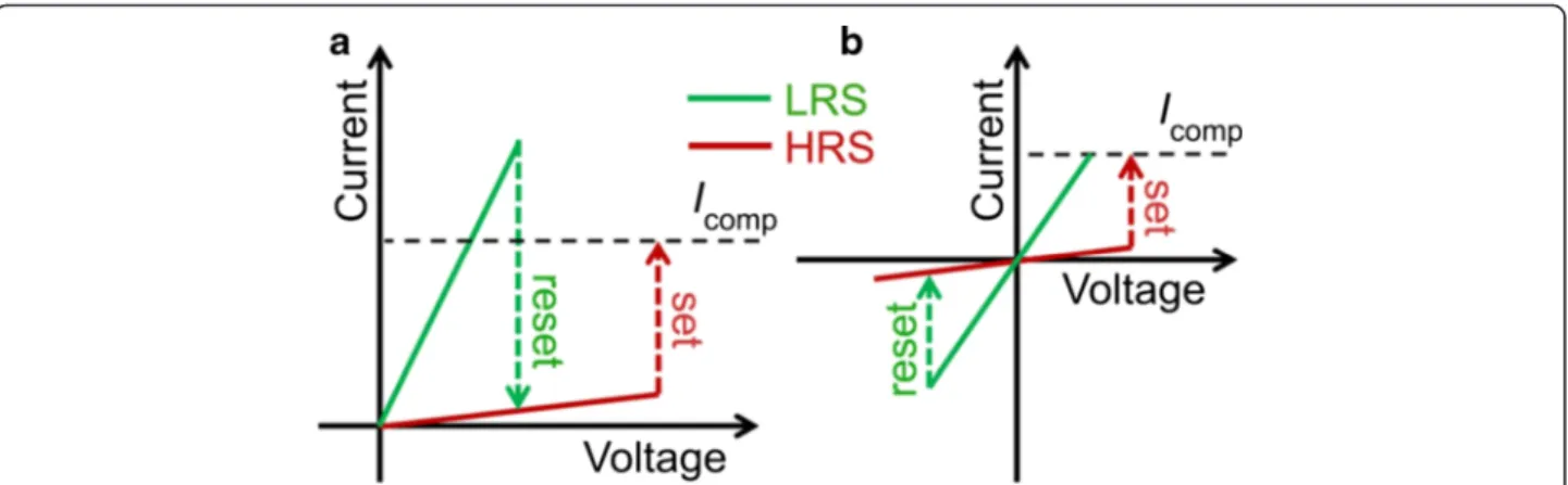
Resistive memory operates under either unipolar or
bi-polar operation mode. In unibi-polar mode, depicted in
Fig. 2a, set and reset processes occur in the same bias
polarity. Conversely, in bipolar mode, opposite bias
po-larities are required to set and reset a device, as depicted
in Fig. 2b. These modes are dependent on device
struc-ture [44, 45, 83] and electrical operation setup [31, 84].
However, coexistence of bipolar and unipolar in the
same device was also reported [85–88]. Nevertheless,
general understanding on unipolar and bipolar modes
can be concluded upon the factors that trigger the reset
process. In unipolar, Joule heating is the main driving
force to rupture a CF during reset, whereas in bipolar,
dissolution of CF is due to the migrating charged
spe-cies, yet Joule heating still contributes to accelerate the
migration [42, 45].
Generally, based on the chemical effects involved in
the switching process, RRAM can be classified as
elec-trochemical metallization memory (ECM) and valence
change memory (VCM) [44]. ECM, also known as
con-ductive bridge CBRAM, relies on an electrochemically
active metal electrode [42] such as Ag, Cu, or Ni, to
form metal cation-based CF. On the other hand, CF in
VCM cell is composed of oxygen vacancies defects,
in-stead of metal atoms, due to anion migration within the
storage material itself [31]. This CF size in the range of
20–30 nm strongly depends upon the amount of current
flowed during forming and set [45, 89].
In filamentary model, the set current mainly flows
through the CF [46]. The filament size is considerably
smaller than electrode area that leads to localized
con-duction effect; thus, LRS is independent on electrode
size [46, 86, 90]. Apart from the filamentary model,
Fig. 1Schematic of conductor/insulator (or semiconductor)/conductorsandwich structure [43]
homogeneous interface-type model was also proposed in
switching mechanism of VCM cell [43]. In homogeneous
interface-type model, both set and reset current flow
homogenously over the entire electrode area; thus, LRS
and HRS are proportional to the electrode area [44]. The
conduction is determined by the field-induced change of
the Schottky barrier height at the electrode/storage
ma-terial interface [42, 44]. Interface-type device can be
de-signed by sandwiching the storage material with Ohmic
and Schottky contacts [43, 91] or modulating oxide/
oxide interface in multilayer device [83].
The filamentary switching can be transformed into
homogeneous switching [84] by modulating the
meas-urement parameters. Figure 3 shows the transformation
of filamentary into homogeneous switching in a typical
Pt/ZnO/Pt device [84]. The transformation was
con-ducted by introducing a reverse sweep bias with high
Icomp
after initiating unipolar switch leading to the
formation of oxygen-defective region near the bottom
electrode, as depicted in the inset of Fig. 3b [84]. This
region can also be modulated simply by applying various
Icomp
or
reset
voltage
(Vreset);
hence,
multilevel
characteristic was observed. Multilevel characteristics
having more than two resistance states can be an
effect-ive way to increase storage density besides device size
scaling [42, 92]. Homogeneous switching dependent on
device area guarantees a sufficient current to maintain
reliable operation, whereas filamentary may suffer from
switching instability in a scaled down device [84].
Never-theless, filamentary exhibits superior retention due to
the aligned conducting channel, since in homogenous
switching, oxygen vacancies from interface tend to
dif-fuse back to the bulk through the grain boundaries
lead-ing to poor retention performance [91].
Origin of Conducting Filament
CF is formed in ECM
cell when a positive bias applied on an active electrode
that leads to an anodic dissolution at anode/storage
ma-terial interface, resulting in metal cations diffusing
to-ward the opposite electrode [93]. The cation transfer and
mobility are controlled by electron dose, Joule heating,
and structural quality of the storage material [93, 94].
Mo-bility also controls the reduction process occurring either
before or after the cations reach the opposite electrode
Fig. 2Schematic I-V curves ofaunipolar andbbipolar switching. Icompdenotes the compliance current, which is adopted during set process to prevent permanent breakdown [43]Fig. 3Transformation of filamentary into homogeneous resistive switching by applying reversed bias with high (Icomp) in Pt/ZnO/Pt device. The insets in the left and right figures are TEM images of the device before and after transformation, respectively [84]
[43, 93]. These cations then reduce in the form of tiny
metal clusters that grow from anode to cathode or vice
versa depending on the mobility [43, 93, 95].
Thus, the construction of these tiny metal clusters across
the storage material leads to the formation of a conducting
metal bridge (filament) that behaves as an electron
conduc-tion channel between the electrodes [93, 94]. During reset
or rupture process, Joule heating is mostly dominated at
the narrowest part of the filament, which is most known as
the filament dissolution process [43, 95].
Unlike ECM cell that relies on metal cation migration
from active anode, the formation of CF in VCM cell is
due to the migration of oxygen ions and oxygen vacancy
defects that generated within the storage material itself.
When a positive bias is applied on anion-active anode,
oxygen ions move toward anode; reversely, oxygen
va-cancies move toward cathode [43]. The percolation of
oxygen vacancies across the storage material acts as an
acceptor for electron carriers [43]. Yet, the physical
mechanism of CF formation in VCM is a good area of
research.
Kwon et al. [96] suggest that CF in TiO2
system is an
ordered structure, Magnéli phase, that is spontaneously
formed under electric field and thermal effect. Magnéli
phase possess high electron conductivity near room
temperature [97]. However, Kwon et al. [98] argue that
the formed Magnéli phase is just as a virtual electrode
while set and reset processes are the rejuvenation and
dissolution of Wadsley defects, respectively. Wadsley defect
can be considered as a missing plane of oxygen atoms in
TiO2
rutile structure [98]. Similarly, Yoon et. al. [99, 100]
suggest that a localized TiO2
−xlayer may act as an active
switching region where as rejuvenation and dissolution of
Magnéli phase as a switching filament may be insignificant.
Nevertheless, formation of a certain conducting phase, like
a Magnéli phase in TiO2, may not be possible in ZnO since
it has no stable suboxide phase [101]. Therefore, other
mechanisms on the formation of CF could be dominant.
Recent theoretical studies [102, 103] on the formation
of CF in ZnO VCM cell suggest that the generated
oxy-gen vacancies moves toward cathode and transform their
2+ charges to neutral thus weaken the Schottky barrier
at ZnO/Pt interface, meanwhile the Zn
2+is reduced to
O-deficient Zn ions (Zn
(2-n)+) around the respective
re-gion. The chemical reaction for these processes can be
expressed as [102];
O
xo
→
V
Oooþ
1
=
2O
2þ
2
e
−ð
1
Þ
V
Ooo
þ
2
e
−→
V
xoð
2
Þ
Zn
2þþ
ne
−→
Zn
ð2−nÞþð
3
Þ
where
O
xo;
V
Ooo;
O
2;
e
−;
V
x
o
;
Zn
2þ;
and Zn
ð2−nÞþare a neutral
charge of oxygen ion in O site, a doubly positive charge
of O vacancy, oxygen gas, a singly negative charge of an
electron, a neutral charge of oxygen vacancy, a doubly
positive charge of zinc ions, and a reduced positive
charge of zinc ions, respectively. Equations
1
,
2
, and
3
are chemical reaction for the generation of oxygen
va-cancies, transformation of oxygen vacancies to neutral
state, and reduction of zinc metal ions, respectively.
The aligned neutral oxygen vacancy (neutral oxygen
vacancy filament), therefore, leads to formation of high
conductive Zn
(2−n)+filament [102]. Thus, the electrons
prefer to conduct trough this metallic filament due to
the lower chemical valence state [102, 103]. Conversely,
the transformation of oxygen vacancies charge from 2+
to neutral by opposite voltage polarity (bipolar) or Joule
heating (unipolar) will lead to oxygen vacancies diffuse
from their configuration to other sites, in other words,
disruption of filament made by oxygen vacancy [102].
Chen et al. [69, 89] directly observed CF in ZnO cell
by utilizing in situ TEM (transmission electron
micro-scope) technique. It was observed that once the oxygen
vacancies reach a certain critical density, a newly
gener-ated ordered crystalline phase is formed. Figure 4 shows
the reset process and structure identification of a CF in
Pt/ZnO/Pt cell [89]. It was found that the CF region was
identified as a Zn-dominated ZnO1
−xmetallic phase
[89], confirming the formation of zinc metallic filament
[102, 103]. This metallic phase can be ruptured when
the oxygen ions migrate to this metallic phase region
and convert the Zn-dominated ZnO1
−xphase back to
ZnO phase [69, 89]. Consequently, this evidence shows
that the oxygen ion migration plays a critical role in the
formation and disruption of a CF.
Despite various advance imaging techniques that have
been employed to understand the nature of CF in both
metal oxide-based ECM and VCM cell such as scanning
transmission x-ray microscope (STXM) [104–106], TEM
[69, 89, 93, 94, 96, 98, 107, 108], and C-AFM
(conduct-ive-atomic force microscope) [56, 68, 77, 78, 109–114],
the relationship between retention behavior and
evolu-tion of CF is still less discussed.
Effect of Electrodes in ZnO-Based RRAM Devices
ZnO is generally n-type high-bandgap semiconducting
materials. Although the origin of its electron
conductiv-ity is still debatable, Zni (zinc interstitial) and Vo
(oxy-gen vacancy) defects are considered to be responsible for
the low resistance [115, 116]. Abundant amount of these
defects may result in insufficient switching properties.
Therefore, several attempts have been reported to
im-prove ZnO as a switching layer, such as stacked with
various metal electrodes [117–128], controlled its
growth deposition [52, 129–133], post-thermal treated
[134, 135], doped with various elements [56, 85–87, 90,
91, 110, 136–152], and embedded/multilayered with
various metalsor oxides [55, 83, 153–159].
According to electrochemical behavior of electrodes, the
types of the electrodes that commonly stacked with
stor-age material are inert, oxidizable, and active metals. Inert
electrode, such as Pt, Ru, or Au, as a cathode may create
high interface barrier to induce resistive switching
proper-ties [160]. High work function of these inert electrodes
at-tributed to higher ON/OFF ratio [161]. As an anode,
however, the high work function may not play important
role; nonetheless, due to its inert behavior, the electrode
has good electrochemical behavior that leads to efficient
redox reaction [127]. Unfortunately, the preservation of
oxygen in inert electrode is limited [37, 162, 163]. Unlike
inert electrode, oxidizable metal electrode, as an anode,
has an advantage of having oxygen reservoir behavior.
This metal electrode tends to form thin interfacial metal
oxide layer at top electrode (TE)/ZnO interface. The
inter-facial layer controls the oxygen outflow to the
environ-ment during SET process; thus the well-preserved oxygen
leads to long endurance [164]. However, even though
there are a number of oxidizable metal available, still, an
appropriate anode for ZnO-based resistive memory needs
to be selected carefully.
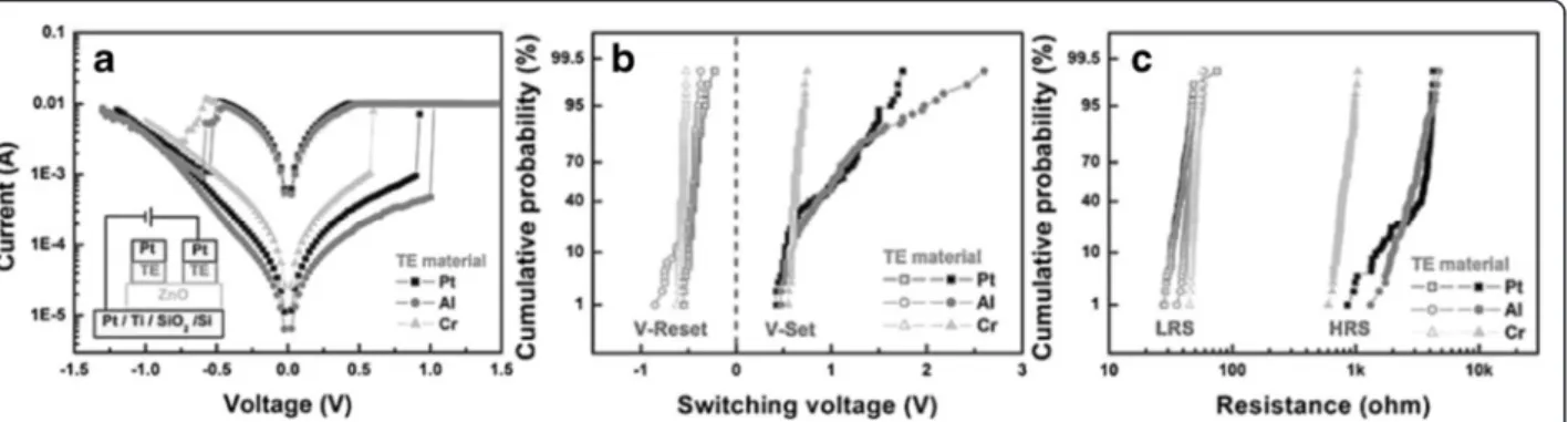
I-V switching characteristics of various metal top
elec-trodes based having TE/ZnO/Pt structure is shown in
Fig. 5a. Despite both Al and Cr are able to create AlOx
and CrOxas oxygen reservoir at the interface,
respect-ively, however, obvious device instability is exhibited in
devices made with Al electrode, as shown in Fig. 5b, c.
Fig. 4In situ TEM images of the reset process using the unipolar resistive switching method.aThe start of recording;bintermediate state;cfinal state of the ruptured filament after the reset process.dThe corresponding I-V curve inred; theblue linecorresponds to the forming process as a comparison.eThe other conductive filament in the same in situ specimen, indicating that the switching behavior is caused by multi-filament formation and rupture.fThe selected area diffraction pattern of the conductive filament in Fig. 2e. The Zn (101) diffraction spot is marked with thered circle.gThe corresponding dark-field image obtained from the diffraction spot marked as a circle in the diffraction pattern (f).hThe Moire fringes can be observed at the disrupted region from a high-magnification TEM image.iThe HRTEM image along the (110) zone axis in the disrupted region, revealing that the conductive filaments were converted back to ZnO1−x.jThe HRTEM of the“zinc”conductive filament along the (231) zone axis has been identified.kSolid-sphere model of ZnO in a wurtzite structure along the (110) zone axis. The coordinate lines are the unit cell vectors.lSolid-sphere model of zinc in a HCP structure along the (231) zone axis. The three-dimensional schematic illustrations of ma ZnO unit cell andna zinc unit cell, respectively, showing that the zinc atoms position remain the same as the oxygen ions diffuse out [89]Similar standard free energy of formation of oxide
Δ
G
ofbetween Cr and Zn leads to efficient redox process [163].
Conversely, large difference
Δ
G
ofbetween Al and Zn leads
to less oxygen can be supplied from AlOx
to rupture the
oxygen vacancies filament during reset process; in
addition, the morphology of AlOx interface layer is found
to be rough, which leads to device instability [163]. Hence,
oxidizable metal having close
Δ
G
ofwith ZnO and smooth
interfaces are crucial in selecting appropriate anode for
re-liable ZnO RRAM device [163, 165]. Among these three
top electrodes (Cr, Al, and Pt), Cr top electrode shows
bet-ter performance compared to others.
In ECM devices, however, the resistive switching
be-havior depends upon the electronegativity and ionic size
of the active anodes which determine the mobility of
metal cations inside ZnO [161]. The use of low
electro-negativity and small ionic size of the active anodes result
in easier formation and rupture of CF in ECM devices
compared to VCM devices [161]. Therefore, set and
re-set voltages in ECM are lower than that in VCM.
Never-theless, it is reported that a high electronegativity of Au
may also behave as active metals [108]; in addition, the
omission of Ni or Ag atoms diffusion in CF formation is
also reported [166, 167]; this phenomena may relate to
different ZnO film quality, device geometry, and
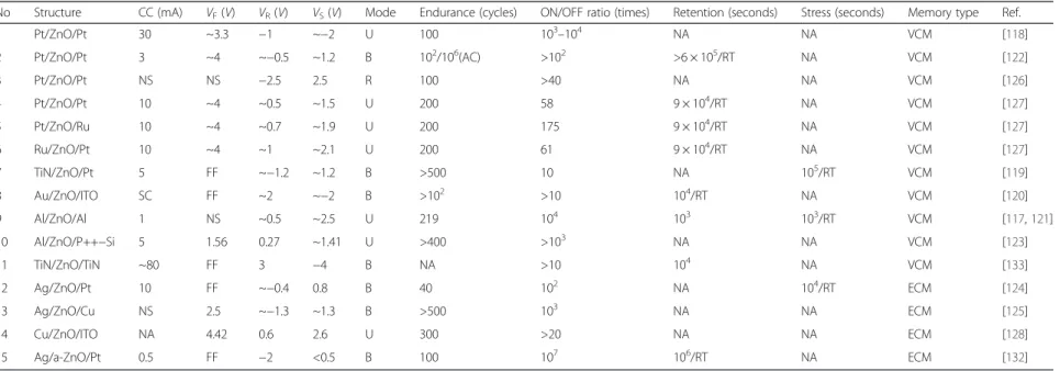
oper-ation method. The major device parameters as a
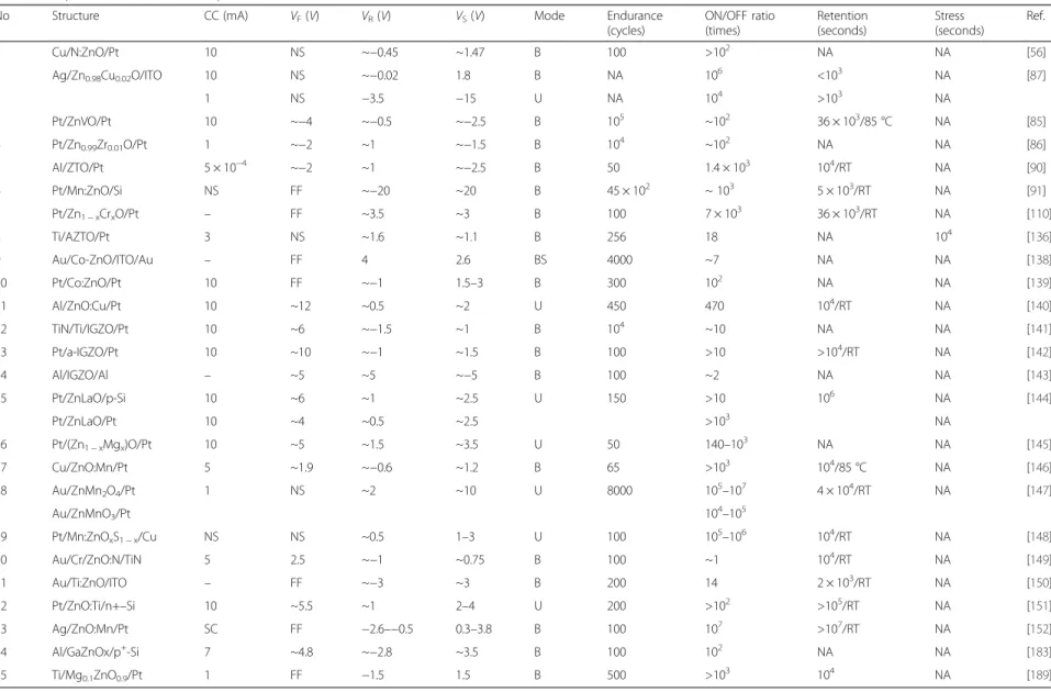
func-tion of different metal electrodes are summarized in
Table 1. The best reported structures having a good
combination between low power, endurance, and
reten-tion performance so far are Pt/ZnO/Pt [122] and
Ag/a-ZnO/Pt [132] for VCM and ECM devices, respectively.
Effect of Deposition Parameter in ZnO-Based RRAM Devices
Besides electrodes, microstructural properties and
de-fects in ZnO film strongly affect the switching behavior
as well. Zinc interstitial and oxygen vacancy native
de-fects behave as self dopants in pure ZnO [115, 116, 168].
Excessive defect concentration leads to high leakage
current and degradation of device performance [169].
Controlled ZnO film growth is required in order to
fab-ricate good quality film having highly oriented growth
and less native defects. Several methods have been
re-ported to fabricate high-quality ZnO film for RRAM
ap-plication, such as ALD [133, 170–172], MOCVD [173],
PLD [135], electrospray [125], electrodeposition [167],
spin-coating [174], DC-sputtering [129, 131], and
RF-sputtering [52]. Yet, RF-sputtering is the most commonly
used technique due to their thickness controllability,
large area uniformity, low temperature, and less-toxic
process. ZnO film properties can be simply controlled
by modulating Ar/O2
flow ratio during sputtering.
Figure 6 depicts the switching parameter of VCM and
ECM unipolar devices made with various Ar/O2
flow
ra-tio. ON/OFF ratio tends to increase as oxygen flow ratio
increase. ZnO grown on higher oxygen flow condition
reduces the formation of oxygen vacancy defects which
can generate more free carriers, thus leading to higher
HRS resistance. In terms of device stability, as oxygen
flow increases VCM, devices tend to be unstable. As
oxygen flow increases, smaller grains are grown in the
ZnO film that leads to higher number of grain
boundar-ies and multiple conducting path [52], leading to
unstability. Excessive conductive filaments result in
un-stable set/reset process in RRAM devices [54].
Con-versely, higher oxygen flow results in better stability in
ECM devices due to lower amount of pre-existing
oxy-gen vacancy defects in ZnO film; thus, the electron
con-duction controlled by metallic bridge will be more
dominant than the oxygen vacancies in ECM devices.
Therefore, less reset competition between the metal
bridge and oxygen vacancies during Joule heating
process may lead to better stability. In addition,
post-thermal treatment after deposition can also be employed
to improve crystallinity and adjust the defect
concentra-tion in ZnO film. The decreasing of the native defects
and increasing of crystallinity in ZnO film after air or
oxygen ambient annealing may enhance ON/OFF ratio
in ECM and VCM devices [134, 135]. Yet, this treatment
may also increase the forming voltage; a high forming
Fig. 5aTypical I-V characteristics of various electrode materials with TE/ZnO/Pt structures. Theinsetshows the schematic structure for electrical measurement of TE/ZnO/Pt structures.bThe cumulative probability of V-Set and V-Reset.cThe cumulative probability of HRS and LRS [163]Table 1
ZnO-based RRAM fabricated with various metal electrodes in published literature
No Structure CC (mA) VF(V) VR(V) VS(V) Mode Endurance (cycles) ON/OFF ratio (times) Retention (seconds) Stress (seconds) Memory type Ref.
1 Pt/ZnO/Pt 30 ~3.3 −1 ~−2 U 100 103–104 NA NA VCM [118]
2 Pt/ZnO/Pt 3 ~4 ~−0.5 ~1.2 B 102/106(AC) >102 >6 × 10⁵/RT NA VCM [122]
3 Pt/ZnO/Pt NS NS −2.5 2.5 R 100 >40 NA NA VCM [126]
4 Pt/ZnO/Pt 10 ~4 ~0.5 ~1.5 U 200 58 9 × 10⁴/RT NA VCM [127]
5 Pt/ZnO/Ru 10 ~4 ~0.7 ~1.9 U 200 175 9 × 10⁴/RT NA VCM [127]
6 Ru/ZnO/Pt 10 ~4 ~1 ~2.1 U 200 61 9 × 10⁴/RT NA VCM [127]
7 TiN/ZnO/Pt 5 FF ~−1.2 ~1.2 B >500 10 NA 105/RT VCM [119]
8 Au/ZnO/ITO SC FF ~2 ~−2 B >102 >10 104/RT NA VCM [120]
9 Al/ZnO/Al 1 NS ~0.5 ~2.5 U 219 104 103 103/RT VCM [117,121]
10 Al/ZnO/P++−Si 5 1.56 0.27 ~1.41 U >400 >103 NA NA VCM [123]
11 TiN/ZnO/TiN ~80 FF 3 −4 B NA >10 104 NA VCM [133]
12 Ag/ZnO/Pt 10 FF ~−0.4 0.8 B 40 102 NA 104/RT ECM [124]
13 Ag/ZnO/Cu NS 2.5 ~−1.3 ~1.3 B >500 103 NA NA ECM [125]
14 Cu/ZnO/ITO NA 4.42 0.6 2.6 U 300 >20 NA NA ECM [128]
15 Ag/a-ZnO/Pt 0.5 FF −2 <0.5 B 100 107 106/RT NA ECM [132]
Unless specified, endurance was measured using DC voltage sweeping mode
CCcurrent compliance,VFforming voltage,VRreset voltage,VSset voltage,SCself-compliance,FFforming free,Uunipolar,Bbipolar,RTmeasured at room temperature,NAdata not available,NSnot specified
Simanjunt
ak
et
al.
Nanoscale
Research
Letters
(2016) 11:368
Page
7
of
voltage may generate large size and excessive number of
CFs that may lead to switching instability [134, 135].
Besides Ar/O2
flow ratio, switching layer thickness also
plays a crucial role on the switching parameter in RRAM
operation. Figure 7 shows the effect of ZnO thickness on
the resistive switching performance of ECM and VCM
unipolar devices [130, 131]. Higher forming voltage is
re-quired for thicker devices that are simply due to the
lon-ger CF that needs to be created between the electrodes.
Reset voltage of VCM devices is insensitive to the
thick-ness. However, Vset in VCM devices increases as ZnO
thickness increases, due to higher crystallinity in thicker
film. The higher crystallinity film having a larger grain size
and lower density of dislocations may provide less
con-duction path during filament formation [130]. Contrarily,
set and reset voltages of ECM devices are not directly
af-fected by the structural properties due to oxide thickness.
Similar phenomenon is also observed in doped ZnO
bipo-lar ECM devices [146]. This phenomenon may arise due
to the Joule heating effect taking place at a critical area
where it is not significantly altered with the thickness
vari-ation [146]. It is also important to note that the
Fig. 7aSwitching voltage variation of the Al/ZnO/Al structure ReRAM device a with ZnO film thickness [130], (b) forming, set, and reset voltages as a function of film thickness for Cu/ZnO/n+-Si device. Each data point was extracted from five devices. The inset of (b) is the thickness dependence on occurrence probability of the initially ON state for as-deposited ZnO. The occurrence probabilities were collected from 25 devices for each point [131]
Fig. 6Distribution of (a) set/reset voltages andbresistance ratios of HRS/LRS at different O2pressure ratio in Pt/ZnO/Pt device [52].cAverage HRS and LRS resistances andddistribution of reset current for ZnO deposited at different oxygen contents in Cu/ZnO/n+-Si device [129]
improvement of ON/OFF ratio after slight adjustment in
Ar/O2
ratio or post-annealing treatment seems more
obvi-ous in VCM than ECM devices. Consequently, it opens
another area and challenge on how to modulate the Joule
heating effective region in ECM cell.
Effect of Doping in ZnO-Based RRAM Devices
Nevertheless, controlled deposition parameter and
post-thermal treatment on resistive layer may be not as
ef-fective as doping technique to fully adjust the defect
concentration. Various dopant elements, such as Al
[137, 175, 176], B [177], Co [138, 139, 169, 178], Cr
[110, 158], Cu [87, 140, 179], Fe [180, 181], Ga [112,
182, 183], La [144], Li [184, 185], Mg [55, 111, 145,
186–190], Mn [91, 146–148, 191–195], N [56, 149], Ni
[196], S [197], Sn [90, 198], Ta [199], Ti [150, 151], V
[85], and Zr [86], that have been reported may exhibit
decent switching performance. ZnO-based RRAM with
multi-element doping, such as Al-Sn [136, 200], Ga-Sn
[201], and In-Ga [141–143, 202–208], is also proposed.
The effect of doping on the resistive switching
perform-ance is summarized in Table 2. Among the reported
de-vices, devices having Mn dopant exhibit not only good
endurance but also long retention performance.
The concentration of native and extrinsic defects
in-duced by doping can be efficiently tuned by considering
the defect generation chemistry. The formation of native
defects in nonstoichimetric ZnO can be expressed using
Kroger-Vink notation as follows [169, 209]:
Zn
xZnþ
2
O
xo↔
Zn
ooiþ
O
2ð Þ þ
g
2
e
′
ð
4
Þ
O
x o↔
1
2
O
2ð Þ þ
g
V
O ooþ
2
e
′
ð
5
Þ
where Zn
xZnand Zn
iooare a neutral charge of a Zn ion
in a zinc site and a doubly positive charge of a Zn
ion in an interstitial site, respectively. Excessive Zn
iooand
V
Oooconcentration may deteriorate switching
per-formance [
145
,
169
]. Therefore, the purpose of ZnO
doping is to promote compensator defects and to
de-crease the native defect concentration. For example,
the formation of compensator defects due to Co
dop-ant can be expressed using Kroger-Vink notation as
follows [
169
,
209
]:
Co
ϰO
γ↔
XZnO
ϰ
Co
Znxþ
ϰ
O
xoþ
ð
γ−ϰ
Þ
O
i00
þ
2
h
oÞ
ð
6
Þ
Co
ϰO
γ↔
YZnO
ϰ
Co
Znxþ
γ
O
xoþ
ð
γ−ϰ
Þ
V
00
Zn
þ
2
h
oð
7
Þ
where Co
xZn;
O
i′′;
V
Zn′′, and
h
oare a neutral charge of
Co ion in a Zn site, a doubly negative charge of an O
ion in an interstitial site, a doubly negative charge of a
Zn vacancy, and a singly positive charge of a hole,
re-spectively. As the result, oxygen concentration and
insu-lating behavior in resistive layer are increased and thus
improve ON/OFF ratio [
169
]. However, excessive dopant
may deteriorate switching cycles and stability
perform-ance [
110
,
143
,
151
,
169
,
175
,
179
,
190
]. The
deterior-ation occurs due to the weakening of c-axis-textured
structure after increasing dopant concentration [
169
].
C-axis texture is a beneficial characteristic of ZnO that
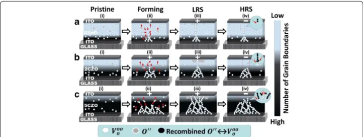
plays an important role to confine CF [127]. Figure 8 shows
the schematic of CF development in various concentration
of Co-doped ZnO resistive layer [169]. The study suggests
there is a trade-off in reducing native defects and
maintain-ing c-axis-textured structure in ZnO-based RRAM [169].
Therefore, the trade-off should be well adjusted for
achiev-ing a decent endurance performance.
It can also be noted that such trade-off may limit the
fabrication of fully c-axis-textured growth.
Conse-quently, the
“hunt”
for finding suitable doping element
and technique that allow the increasing of both acceptor
defects and microstructural quality is still needed.
Employing a p-type doping element such as nitrogen
may increase both acceptor concentration and
micro-structural quality, thus improving RRAM performance
[56, 149]. In addition, p-type ZnO-based RRAM still has
not received sufficient attention yet.
Employing an amorphous resistive layer may also
avoid the formation of excessive and branching of CF
due to the lack of grain boundary structure. Several
ef-forts have been reported to fabricate amorphous
ZnO-based RRAM, such as by doping [90, 141–143, 177, 198,
201–203, 205–208], hydrogen peroxide treatment [183],
and deposition parameter optimization [132].
ZnO-Based Complementary RRAM
Although doping technique can be considered as the
simplest way to improve switching properties, embedded
and multilayered structure still receive great attention
due to easy modulation of switching behavior in the
switching layer. Table 3 shows the summary of the
im-portant switching parameters of multilayered and
em-bedded ZnO-based RRAM. Multilayer structure can be
employed not only to improve switching performance
but also to generate different peculiar switching
charac-teristics. By employing proper electrical programming to
control formation and rupture of CF at the particular
switching layer, complementary switching (CS)
charac-teristics can be achieved. CS is a unique switching
char-acteristic that is useful for avoiding sneak path
disadvantage in a three-dimensional crossbar RRAM
ap-plication [153, 154].
Figure 9a shows the CS characteristic of TiN/MgZnO/
ZnO/Pt double layer memory device [153]. The CS
char-acteristic can be obtained under proper programming
Table 2
Doped ZnO-based RRAM in published literature
No Structure CC (mA) VF(V) VR(V) VS(V) Mode Endurance (cycles)
ON/OFF ratio (times)
Retention (seconds)
Stress (seconds)
Ref.
1 Cu/N:ZnO/Pt 10 NS ~−0.45 ~1.47 B 100 >102 NA NA [56]
2 Ag/Zn0.98Cu0.02O/ITO 10 NS ~−0.02 1.8 B NA 106 <103 NA [87]
1 NS −3.5 −15 U NA 104 >103 NA
3 Pt/ZnVO/Pt 10 ~−4 ~−0.5 ~−2.5 B 105 ~102 36 × 103/85 °C NA [85]
4 Pt/Zn0.99Zr0.01O/Pt 1 ~−2 ~1 ~−1.5 B 104 ~102 NA NA [86]
5 Al/ZTO/Pt 5 × 10⁻⁴ ~−2 ~1 ~−2.5 B 50 1.4 × 10³ 104/RT NA [90]
6 Pt/Mn:ZnO/Si NS FF ~−20 ~20 B 45 × 102 ~ 103 5 × 10³/RT NA [91]
7 Pt/Zn1−xCrxO/Pt – FF ~3.5 ~3 B 100 7 × 10³ 36 × 103/RT NA [110]
8 Ti/AZTO/Pt 3 NS ~1.6 ~1.1 B 256 18 NA 104 [136]
9 Au/Co-ZnO/ITO/Au – FF 4 2.6 BS 4000 ~7 NA NA [138]
10 Pt/Co:ZnO/Pt 10 FF ~−1 1.5–3 B 300 102 NA NA [139]
11 Al/ZnO:Cu/Pt 10 ~12 ~0.5 ~2 U 450 470 104/RT NA [140]
12 TiN/Ti/IGZO/Pt 10 ~6 ~−1.5 ~1 B 104 ~10 NA NA [141]
13 Pt/a-IGZO/Pt 10 ~10 ~−1 ~1.5 B 100 >10 >104/RT NA [142]
14 Al/IGZO/Al – ~5 ~5 ~−5 B 100 ~2 NA NA [143]
15 Pt/ZnLaO/p-Si 10 ~6 ~1 ~2.5 U 150 >10 106 NA [144]
Pt/ZnLaO/Pt 10 ~4 ~0.5 ~2.5 >103 NA
16 Pt/(Zn1−xMgx)O/Pt 10 ~5 ~1.5 ~3.5 U 50 140–103 NA NA [145]
17 Cu/ZnO:Mn/Pt 5 ~1.9 ~−0.6 ~1.2 B 65 >103 104/85 °C NA [146]
18 Au/ZnMn2O4/Pt 1 NS ~2 ~10 U 8000 105–107 4 × 10⁴/RT NA [147]
Au/ZnMnO3/Pt 104–105
19 Pt/Mn:ZnOxS1−x/Cu NS NS ~0.5 1–3 U 100 105–106 104/RT NA [148]
20 Au/Cr/ZnO:N/TiN 5 2.5 ~−1 ~0.75 B 100 ~1 104/RT NA [149]
21 Au/Ti:ZnO/ITO – FF ~−3 ~3 B 200 14 2 × 10³/RT NA [150]
22 Pt/ZnO:Ti/n+–Si 10 ~5.5 ~1 2–4 U 200 >102 >105/RT NA [151]
23 Ag/ZnO:Mn/Pt SC FF −2.6–−0.5 0.3–3.8 B 100 107 >107/RT NA [152]
24 Al/GaZnOx/p+-Si 7 ~4.8 ~−2.8 ~3.5 B 100 102 NA NA [183]
25 Ti/Mg0.1ZnO0.9/Pt 1 FF −1.5 1.5 B 500 >103 104 NA [189]
NSnot specified,CCcurrent compliance,SCself-compliance,FFforming free,Uunipolar,Bbipolar,BSbistable,VFforming voltage,VRreset voltage,VSset voltage,RTmeasured at room temperature,NAdata not available
Simanjunt
ak
et
al.
Nanoscale
Research
Letters
(2016) 11:368
Page
10
of
steps, which can vary from device to device. For the
TiN/MgZnO/ZnO/Pt memory device structure, the
pro-gramming steps are as follows [153]: firstly, the device is
operated
under
common
counterclockwise
bipolar
switching mode. When the device is on LRS (set), low
negative bias of
−
1 V was applied on top electrode (TE);
consequently,
oxygen
vacancies
move
toward
the
MgZnO layer, by leaving some filament gap in the ZnO
layer and make the device in HRS (reset). This process is
called second electroforming. When low positive bias of
~0.6 V is applied on TE (Vth1), the oxygen vacancies
re-pulse back to ZnO layer and resulted both layers in LRS
(set); however, as the bias is continuously applied to
reach ~1 V (Vth2), the oxygen vacancy filament size at
MgZnO layer is reduced and ruptured. Similarly, the
same mechanism may apply with the negative bias. Low
negative bias of ~
−
0.6 V (Vth3) may repulse the oxygen
vacancies from ZnO layer to MgZnO layer and form the
filament at the MgZnO layer; consequently, both layers
are in LRS (set). As the negative bias is continuously
ap-plied to reach ~
−
1 V (Vth4), the oxygen filament size at
ZnO layer is gradually ruptured and makes the device
back to HRS (reset) [153].
Another method to produce CS characteristic is by
simply reversely stacking two cell memories. Figure 9b, c
shows the resistive switching characteristics of Pt/ZnO/
ZnWOx/W (cell A) and W/ZnWOx/ZnO/Pt (cell B)
memory, respectively [154]. These devices can only be
set (LRS) and reset (HRS) by applying negative and
posi-tive bias at the Pt electrode, respecposi-tively. Figure 9d
shows the CS characteristics of Pt/ZnO/ZnWOx/W/
ZnWOx/ZnO/Pt device [154]. The CS characteristic on
this device can be generated under programming steps
as followed [154]; initially, both cells are in HRS, called
Fig. 8Schematic of switching mechanism of Zn(1-x)CoxO RRAM with (a) 0 mol%, (b) 2 mol%, and (c) 5 mol% of CoO dopant concentration [169]Table 3
Multilayered and embedded ZnO-based RRAM in published literature
No Structure CC (mA) VF(V) VR(V) VS(V) Mode Endurance (cycles)
ON/OFF ratio (times)
Retention (seconds)
Stress (seconds)
Ref.
1 Pt/ZnO/Ag0.2-Al0.8/Al 1 NS ~0.3 ~2 U 200 >102 NA NA [53]
2 TiN/MgZnO/ZnO/Pt 10/20 ~6 −2 ~1 B 104 >50 3 × 10⁴/RT NA [55]
3 Pt/ZnO/ZrO2/Pt 10 ~−6.5 −4 ~3 B 100 ~5 NA 104 [83]
4 Pt/ZnO/CoOx/ZnO/Pt 10 FF 0.8–1.8 1.5–2.9 B 200 ~102 NA NA [155]
5 Pt/ZnLaO/ZnO/Pt 10 ~3.5 ~1 ~2.3 U 100 ~104 104/65 °C NA [156]
6 Ag/CeO2/ZnO/NSTO 10 NS −5 ~2 B 100 540 103/RT NA [157]
7 Pt/ZnO/Cr/ZnO/Pt NS ~2 −2 3 B 104 ~104 NA 5 × 10³ [158]
8 Pt/(ZnO/Ti/ZnO)1–4/ITO NS FF ~−2.5 ~2 B 320 ~103 >106 NA [159]
9 Ag/GZO/ZnO/Pt/Ti 10 FF 0.55 0.4 B ~40 2 × 10³ 1.1 × 10⁴ NA [182]
10 Pt/TiOx/ZnO/n+-Si NS ~2.8 ~0.5 ~2 U >50 >102 NA NA [286]
11 Al/Al2O3/(ZnO/Al2O3) 10/n-Si/Al
NS FF −7 7 B NA 103
–104 103 NA [287]
NSnot specified,CCcurrent compliance,FFforming free,Uunipolar,Bbipolar,VFforming voltage,VRreset voltage,VSset voltage,RTmeasured at room temperature,NAdata not available
as
“OFF”
state. Then, one of the cells (cell A) is switched
to LRS while cell B can be maintained in HRS by
sweep-ing low negative bias at the TE. At this stage, cell B is
still in HRS because it requires the opposite bias to
switch and act as a voltage divider. As the positive sweep
bias reach ~0.9 V (Vth1), cell B is switched to LRS.
Be-cause the positive bias of ~0.9 V is not enough to switch
the cell A from LRS to HRS, therefore at this stage, both
cells are in LRS. When both cells are in LRS, it is called
as
“ON”
state. Further increase of positive bias to ~1.3 V
(Vth2) leads to reset cell A. At this stage, cells A and B
are in HRS and LRS, respectively, called as
“1”
state. In
order to switch the device back to
“ON”
state, cell A
needs to switch back to LRS by sweeping with negative
bias of ~
−
0.6 V (Vth3); therefore, both cells are in LRS.
Similarly, at this stage, cell B can still maintain its LRS
because ~
−
0.6 V is not enough to switch it to HRS.
However, as the sweep negative bias continues to reach
~
−
1.3 V (Vth4), cell B is switched to HRS. Therefore, at
this stage, cells A and B are in LRS and HRS,
respect-ively, called as
“0”
state. Consequently, four distinct
threshold biases can be applied to obtain CR switching
characteristics [154].
Achieving CS by employing the above methods is very
useful to maintain simplicity of the memory structure
and fabrication. Yet, further investigation is necessary to
expand the potential of these methods for ZnO-based
ECM cell and transparent VCM cell.
ZnO-Based Transparent/Flexible RRAM
Nonvolatile memory structure having high transmittance
in visible light would be useful for the realization of fully
integrated transparent electronics [210, 211]. Employing
wide direct band gap switching materials, transparent
conducting oxide (TCO) electrodes, and transparent
substrate is required to construct invisible RRAM
structure. ITO [54, 176, 212–220], FTO [213], AZO [54,
219, 221], and GZO [222–224] are the commonly used
TCO as electrodes for transparent electronics.
Conduc-tion and interfacial growth properties of TCO are
strongly determined by its fabrication parameter.
How-ever, still few investigations have been conducted to
ex-plain phenomena in RRAM operation due to different
properties of TCO [219, 225–227].
High quality of ZnO resistive switching layer was
de-posited on TCO electrodes using various methods, such
as metal organic chemical vapor deposition (MOCVD)
[212, 223, 224], pulsed laser deposition [213, 218, 221,
222], RF-sputtering [54, 176, 216, 217, 219],
hydro-thermal growth [216], and sol-gel [214, 215, 220].
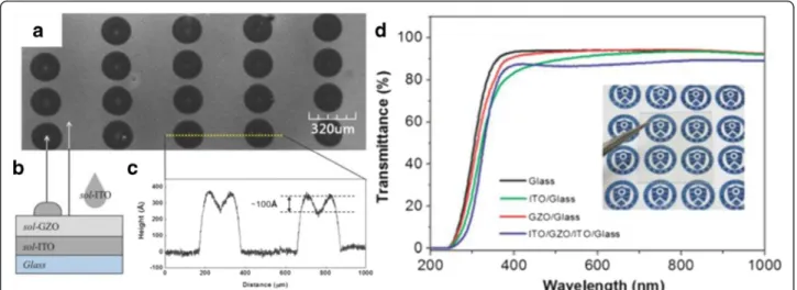
Figure 10a–c demonstrates sol-gel-derived ITO/GZO/
ITO RRAM devices on glass substrate. The device is
fully transparent (~80 %) in the visible region as shown
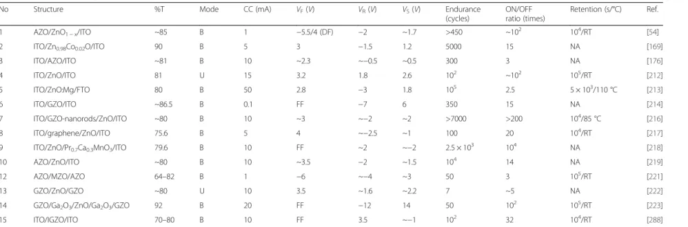
in Fig. 10d. Devices with an average transparency of
above 70 % in visible light region can be considered as
having transparent structure, while semi-transparent is
below 70 % [228]. Table 4 summarizes the switching
pa-rameters and performances of the ZnO-based
transpar-ent RRAM (TRRAM). Multilayer devices made of GZO/
Ga2O3/ZnO/Ga2O3/GZO structures exhibit the highest
transparency with high memory window and long
reten-tion performances [223].
By taking an advantage of low synthetic temperature of
ZnO material, it allows us to fabricate flexible RRAM
(FRRAM) devices on polymer substrate. Flexible
nonvola-tile memory may revolutionize electronics due to its
poten-tial in embedded flexible technologies [229]. Polyethylene
terephthalate (PET) [220, 230, 231], polyethylene
naphtha-late (PEN) [113], polyethersulfone (PES) [232, 233],
poly-mide (PI) [234], and Kapton [235] are commonly used as
polymer substrate; however, flexible RRAM, but not
trans-parent, having metal foil [236] and stainless steel [237]
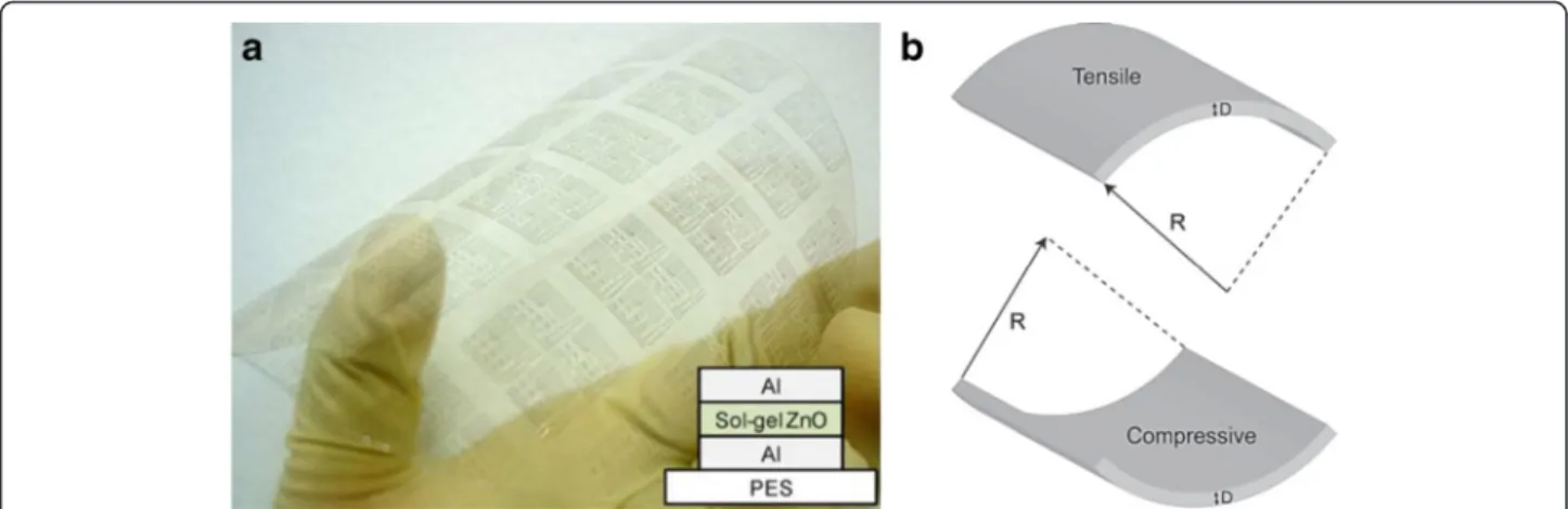
Fig. 9aTypical complementary switching of TiN/MgZnO/ZnO/Pt bipolar memory device.Insetshows I-V curve of one typical switching process plotted in semilogarithmic scale [153].bI-V behaviors of cell A (Pt/ZnO/ZnWOx/W) andccell B (W/ZnWOx/ZnO/Pt).Insetshows the corresponding device configuration.dI-V sweeps of the ZnO/ZnWOx//ZnWOx/ZnOCRS device.Insetshows the device configuration and the corresponding resistive switching for two cells. All the thickness of ZnWOx layer is∼15 nm [154]substrates, was also reported. Figure 11a shows the typical
photograph of flexible RRAM having Al/ZnO/Al structures
fabricated on PES substrate.
Mechanical flexibility is the essential consideration for
flexible memory application feasibility. Reliable memory
window and endurance should be maintained in various
bending condition and after repetitive flexes. Mechanical
parameter related to tensile and compressive strain that
were given upon a memory structure should be taken
into account. Figure 11b shows the schematic illustration
of a flexible substrate receiving tensile and compressive
strain. The strain induced on the surface of a substrate
due to bending can be calculated using Eq. 8 [238];
S
¼
ð
t
Lþ
t
SÞ
ð
1
þ
2
η
þ
x
η
2Þ
2
R
ð
1
þ
η
Þ
ð
1
þ
x
η
Þ
ð
8
Þ
where
S
is strain,
η
=
t
L/
t
S,
t
Lis layer thickness,
t
Sis
sub-strate thickness,
χ
=
Y
L/
Y
S,
Y
Lis the Young
’
s modulus of
the layer, and
Y
Sis the Young
’
s modulus of the substrate.
Nevertheless, there is no definite standard or apparatus
for mechanical flexibility test on RRAM; yet, HRS and
LRS values recorded at different bending radius and
re-peated bending are generally conducted to measure the
memory flexibility.
Employing metal as bottom electrode may help
mechan-ical flexibility of FRRAM due to its higher ductility
proper-ties as compared to oxide electrode. Nonetheless, having
TCO as electrodes is unneglectable when fabricating
trans-parent and flexible RRAM (TFRRAM). TCO films
fabri-cated on flexible substrate may suffer from cracking after
repeated bending. Related to that, compressive stress results
more damage to the films than tensile stress [239]. In order
to minimize this issue, inserting thin metal between TCO
layers has been suggested [233].
Figure 12 shows flexibility test of ITO/ZnO/ITO/PES
and ITO/ZnO/ITO/Ag/ITO/PES TFRRAM. Both
de-vices have shown stable states in various bending radius,
as shown in Fig. 12a. However, devices having single
layer ITO bottom electrode suffer HRS and LRS
degrad-ation upon repeated bending; conversely, devices having
ITO/Ag/ITO multilayer bottom electrode exhibit
excel-lent stability. However, inserting thin metal film between
TCO layers may decrease its transparency [233] and
in-crease the cost of production process [239]. Another
method to enhance bending durability of films while
maintaining the transparency is by employing TCO/
oxide buffer layer/flexible substrate structure [239].
Nonetheless, mechanical flexibility of FRRAM can rely
on not only the ductility of the bottom electrode but
also the resistive layer as well. Interestingly, Al/GOZNs/
ITO/PET FRRAM devices are able to maintain its states
after repeated bending with extreme bending radius of
6 mm [230]. This may suggest that the excellent
mech-anical flexibility of the FRRAM may also be attributed
from the ZnO nanorods-graphene oxide composite
re-sistive layer ductility. Recent report also implied that
employing amorphous InGaZnO (
α
-IGZO) as a resistive
layer may exhibit better mechanical flexibility than
poly-crystalline oxide resistive layer [240]. Yet, further
investi-gation is necessary to explain the influence of ZnO
microstructural
properties
on
resistive
switching
performance under various bending condition. The
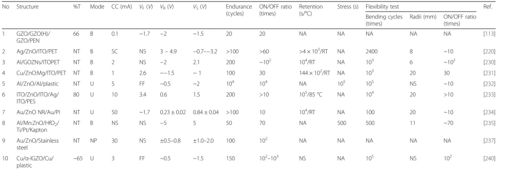
switching parameters of the flexible resistive switching
memory along with flexibility are summarized in
Table 5.
Fig. 10aUV-laser confocal image of inkjet-printed ITO electrodes on a GZO/spin-coated ITO/glass substrate.bSchematic of an all solution processed ITO/GZO/ITO RRAM device.cSurface profile of the top electrodes following theyellow linein (a).dUV-vis transmittance of bare glass (black), ITO/glass (green), GZO/glass (red), and ITO/GZO/ITO/glass (blue). To determine the optical properties, both the ITO bottom and top layers were spin-coated four times, resulting in a film with a thickness of∼30 nm. Theinsetis a photograph of the sol-TRRAM (ITO/GZO/ITO/glass) device. The background is observed through the device without refraction or distortion [214]
Table 4
ZnO-based transparent RRAM in published literature
No Structure %T Mode CC (mA) VF(V) VR(V) VS(V) Endurance (cycles)
ON/OFF ratio (times)
Retention (s/°C) Ref.
1 AZO/ZnO1−x/ITO ~85 B 1 −5.5/4 (DF) −2 ~1.7 >450 ~102 104/RT [54]
2 ITO/Zn0.98Co0.02O/ITO 90 B 5 3 −1.5 1.2 5000 15 NA [169]
3 ITO/AZO/ITO ~81 B 10 ~2.3 ~−0.5 ~0.5 300 3 NA [176]
4 ITO/ZnO/ITO 81 U 15 3.2 1.8 2.6 102 ~102 105/RT [212]
5 ITO/ZnO:Mg/FTO 80 B 50 2.8 −3 1.8 105 2.5 5 × 10³/110 °C [213]
6 ITO/GZO/ITO ~86.5 B 0.1 FF −7 6 350 15 NA [214]
7 ITO/GZO-nanorods/ZnO/ITO ~80 B 10 ~3 ~−2 ~2 >7000 >200 104/85 °C [216]
8 ITO/graphene/ZnO/ITO 75.6 B 5 4 ~−2.5 ~1 100 20 104/RT [217]
9 ITO/ZnO/Pr0.7Ca0.3MnO3/ITO 79.6 B 10 FF ~2 ~−2 2.5 × 10³ 104 NA [218]
10 AZO/ZnO/ITO ~80 B 10 ~3.5 −2 ~1.5 104 14 NA [219]
12 AZO/MZO/AZO 64–82 B 1 −6 ~−4 ~3 50 3 105/RT [221]
13 GZO/ZnO/GZO ~80 U 10 3.5 ~1.6 ~2.2 7 ~5 NA [222]
14 GZO/Ga2O3/ZnO/Ga2O3/GZO 92 B 20 FF −12 14 50 102 105/RT [223]
15 ITO/IGZO/ITO 70–80 B 10 FF 3.5 ~−1 102 32 104/RT [288]
%Tpercentage of transmittance in visible range,Uunipolar,Bbipolar,CCcurrent compliance,FFfree forming,VFforming voltage,VRreset voltage,VSset voltage,DFdouble forming,RTmeasured at room temperature,NAdata not available
Simanjunt
ak
et
al.
Nanoscale
Research
Letters
(2016) 11:368
Page
14
of
Sneak Current Prevention in ZnO-Based RRAM
To resolve the physical scaling issues of conventional
nonvolatile memory devices, crossbar array architecture
has been considered as an attractive construction due to
the scalability, simplicity, and multiple stackability of the
structure. For practical applications, the foremost
bottle-neck of this array architecture is the sneak current path
issue, which leads to read operation error [241].
ZnO-based RRAM having crossbar structures has also
suf-fered from sneak path issue. To suppress the undesired
sneak current, the combination of memory cells with
rectifying or switch devices, such as p-n junction diodes
[242], Schottky diodes [243, 244], threshold switching
devices [245], and transistors [246], is necessary. In this
section, we will discuss about the different aspects to
eliminate sneak path for the ZnO-based RRAM.
Seo et al. [247] reported ZnO crossbar Pt/ZnO/Pt
re-sistive random access memory stacked with
heterostruc-ture diodes of Pt/NiO/ZnO/Pt p-n junction and the Pt/
WO3/ZnO/Pt tunnel barrier diodes for eliminating the
sneak current effect to avoid sneak path current, as
shown in Fig. 13. The fabricated ZnO RRAM device on
glass with a 4 × 4 crossbar array stacked with
hetero-structure diodes is shown in Fig. 13a. Cross-sectional
TEM images of the stacked contact area of different
di-odes is presented in Fig. 13b. Figure 14a, b reveals the
current characteristics of the crossbar array ZnO RRAM
devices combined with the heterostructure diodes. Inset
shows the corresponding energy band diagram of the
di-odes. Stable resistive switching occurring with larger
op-eration voltages is observed due to the additional series
resistance of the heterostructure diodes. However, the
reverse current was effectively suppressed by combining
with the diodes. Similar behavior is also reported by
employing vertically integrated Ag/MgZnO/GaZnO/Au
Schottky diode on Au/FeZnO/MgO/Pt RRAM device
[248]. Usually, diode or transistor or selector needs to be
combined with the RRAM resistor to avoid sneak path
current. But, recently, Fan et al. avoided sneak path
current by fabricating selector-less AZTO-based RRAM
Fig. 11aPhotograph of Al/ZnO/Al flexible resistive memory devices fabricated on PES substrate [232].bSchematic illustrations of the flexible substrate at tensile strain (up) and compressive strain (down), whereRis the bending radius andDis the thickness of the substrate [238]Fig. 12aBending effect of the TFRRAM device. Photograph (shown in the inset) of the device bent atR= 30 mm.bContinuous bending effect of the TRRAM device [233]
Table 5
ZnO-based flexible RRAM in published literature
No Structure %T Mode CC (mA) VF(V) VR(V) VS(V) Endurance (cycles)
ON/OFF ratio (times)
Retention (s/°C)
Stress (s) Flexibility test Ref.
Bending cycles (times)
Radii (mm) ON/OFF ratio (times)
1 GZO/GZO(H)/ GZO/PEN
66 B 0.1 ~1.7 −2 ~1.5 20 20 NA NA NA NA NA [113]
2 Ag/ZnO/ITO/PET NT B SC NS 3–4.9 −0.7–−3.2 >100 >60 >4 × 10³/RT NA 2400 8 ~10 [220]
3 Al/GOZNs/ITOPET NT B 2 NS −2 2.1 200 ~102 104/RT NA 103 6 ~102 [230]
4 Cu/ZnO:Mg/ITO/PET NT B 1 2.6 ~−1.5 ~ 1 100 30 144 × 102/RT NA 103 20 30 [231]
5 Al/ZnO/Al/plastic NT U 5 FF ~0.5 ~2 104 104 NA 105 105 NS ~10 [232]
6 ITO/ZnO/ITO/Ag/ ITO/PES
80 U 10 3.4 0.6 1.5 200 >10 105/85 °C NA 104 20 >10 [233]
7 Au/ZnO NR/Au/PI NT U 50 ~1.7 0.23 ± 0.02 0.84 ± 0.04 >100 10 104/RT NA 100 20 ~10 [234]
8 Al/Mn:ZnO/HfO2/ Ti/Pt/Kapton
NT B NS NS −5 5 50 70 NA 500 500 11 ~70 [235]
9 Au/ZnO/Stainless steel
NT NP 30 NS ±0.5–0.8 ±1.0–2.0 100 102 NA NA NA NA NA [237]
10 Cu/α-IGZO/Cu/ plastic
~65 U 3 FF ~0.5 ~1.5 150 102–103 NS NA 105 NS 102 [240]
%Tpercentage of approximate transmittance in visible range,NTnot transparent,NPnonpolar,CCcurrent compliance,Uunipolar,Bbipolar,SCself-compliance,FFfree forming,Vfforming voltage,Vrreset voltage, Vsset voltage,RTroom temperature,NSnot specified,NAnot available
Simanjunt
ak
et
al.
Nanoscale
Research
Letters
(2016) 11:368
Page
16
of
with a thin insertion layer (2 nm) of Al2O3
[200].
Figure 15a, b shows typical cross-section TEM image of
Ti/AZTO/Al2O3/Pt and the schematic of the fabricated
device, respectively [200]. This device is able to exhibit
read margin with inhabit ratio (IR) of 34 times, as
depicted in Fig. 15c, d [200]. They suggested that Al2O3
may act as an electron barrier where the LRS conduction
is dominated by electron tunnelling mechanism [200].
Nanostructured ZnO-Based RRAM
To reduce the production cost, highly densed RRAM can
be achieved with a maximum size of 4F
2high packing
density by stacking architecture via three-dimensional
crossbar [43, 154, 249]. However, further effort to scaling
down the memory size using unique structure, such as
self-assembly nanostructure, is very attractive. The wide
variety of ZnO morphologies offers novel approach and
understanding to dimensionality dependence on switching
characteristics. Currently, devices employing nanorods/
nanowires [58–75, 216, 250–266], nanobelts [76], and
nanoisland [77, 78] as the switching elements receive
con-siderable interests in developing one-dimensional resistive
memory for ultrahigh density memories.
Figure 16a, b shows the schematic of Pt/ZnO1
−xnanorods/ZnO/Pt device and the cross-sectional SEM
image, respectively [256]. It is believed that ionic defects
prefer to diffuse through the nanorods sidewall due to
higher microstructural defects [252, 253]. Thus, the
Fig. 13aA 4X4 crossbar array ZnO RRAM device stacked with heterostructure diodes. Thelower insetis an image of the entire structure of the device.bCross-sectional TEM images of the stacked contact area [247]Fig. 14aI-V characteristics of the crossbar ZnO RRAM device stacked with (a) a ZnO/NiO p-n junction andbWO3/ZnO tunnel barrier diodes. Insetofaandb: equilibrium band alignment of Pt/NiO/ZnO/Pt and Pt/ZnO/WO3/Pt.Solid circledenotes electron,open circledenotes hole, and arrowsdenote possible conduction mechanisms of carriers. The indicated energy values in the inset diagrams are calculated based on literature values (ref. [284, 285]) [247]
vertically aligned nanorods may induce filament
confine-ment, as depicted in Fig. 16c [256]. However, RRAM
de-vice made with ZnO nanorods layer with low packing
density may suffer from short circuit problem due to
dir-ect contact between top and bottom eldir-ectrodes [254].
Nevertheless, such issue can be avoided by embedding
the nanorods layer in insulating polymers [253] or
syn-thesizing highly densed nanorod film [216, 254]. In
addition to that, employing nanorod layer may
demon-strate surface self-cleaning function against water
Fig. 15aCross-section TEM image of Ti/AZTO/Al2O3/Pt structure.bSchematic of the fabricated memory device structure.cInhibit ratio (IR) of the nonlinear AZTO-based RRAM device.dThe read margin analysis indicate that the proposed IR can extend array to ~3K bits [200]Fig. 16aSchematic of a Pt/ZnO1−xNRs/ZnO TF/Pt resistive switching device.bCorresponding SEM image of a well-aligned ZnO1−XNR with a length of∼150 nm grown on the ZnO film with a thickness of∼100 nm.cSchematic of confined recovery and rupture of conducting filaments by ZnO1−xNRs [256]
contact. Figure 17a, c shows hydrophilicity of ZnO thin
film and hydrophobicity of ZnO nanorods, respectively
[256]. Water-covered endurance characteristics of
de-vices made with nanorod layer exhibit superior
switch-ing performance as compared to device without
nanorods layer, shown in Fig. 17b, d, respectively [256].
This approach not only could avoid short circuit issue
due to surface wetting but also could realize water
resist-ant electronics. Moreover, memory performance of ZnO
nanorods layer based devices can be further improved
by embedding in higher concentration of
polymethyl-methacrylate [267] or surface hydrogen annealing [261].
Resistive memory employing laterally bridged ZnO
nanorods, as shown in Fig. 18a, was developed in order to
fabricate one-dimensional memory nanostructure that can
meet mass production requirement [59]. Figure 18b
dem-onstrates the peculiar unipolar switching [71] in a laterally
bridged nanorod device in which the set voltage is smaller
than the reset voltage that can prevent hard breakdown
due to Joule heating during reset [59]. The formation and
rupture of CF are situated at the nanorod/nanorod
inter-faces so that the actual memory cell size is incredibly
smaller than the length of the nanorod itself.
Another effort to downsizing the physical dimension is
by developing high scalability single nanorod/nanowire
resistive device [60–75]. Orthogonal crossbar or
verti-cally aligned nanorod/nanowire array RRAM devices
could greatly increase storage density due to less
sub-strate area consumption [61, 268]. Although such
ar-rangement has not been reported yet due to its
fabrication complexity, however, the development of
these one-dimensional devices offers a novel
under-standing in resistive switching behavior on low-scale
memory devices. Figure 19a, b shows SEM image and
schematic of the Cu/Zn2SnO4-nanowire/Pd device
struc-ture, respectively [74]. Energy dispersive X-ray (EDX)
analysis suggests that the Cu conductive bridge is
formed in Cu/Zn2SnO4-nanowire/Pd device at the
sur-face of nanorod, as depicted in Fig. 19c, d [74]. The
evi-dence that metal atoms originated from active anode
diffused under voltage bias, which the metal atoms are
mainly distributed on the surface of the nanorod, is also
reported in other ZnO-nanorod-based ECM type devices
[70, 73]. Similarly, oxygen diffusion toward anode on the
surface of a nanorod that leads to filament formation is
also reported in ZnO-nanorod-based VCM type devices
[69]. This confirmed earlier hypothesis that the
forma-tion of CF occurs on the surface/sidewall rather than
within the bulk of the nanorod [252, 253].
Instability and reproducibility of resistive switching in
single ZnO-nanorod/nanowire can be further improved
by utilizing plasma treatment [60, 61] and introduction of
other metal elements, such as Cu [66], Ga, and Sb [62]. It
is also reported that self-compliance and self-rectifying
characteristic can be induced by Na doping on
ZnO-nanowire ECM type devices [70]. Single
nanorod/nano-wire-based devices offer ultra-low operation current, in
the range of pico- to microamperes; however, the high
op-eration voltage, in the range of hecto- to deka-volts, is still
a main challenge in the development of this kind of
resist-ive memory device [60–62, 66, 70, 75]. Despite ZnO:K,Cl
micro/nanowire devices exhibited low operation voltage;
Fig. 17a,bContact angle measurements for surfaces of the ZnO film and the ZnO1−xNRs, respectively.c,dCorresponding endurance tests for two devices measured with coverage of a water droplet at a read bias of 0.1 V, respectively [256]
however, the operation current is in the range of
milliam-peres which is quite high for its class [63]. In another
re-port, low current and voltage operation is exhibited in Ag/
Zn2SnO3-sheated ZnO-core heterostructure nanowire/Ag
device [67]; yet, the fabrication of this heterostructure is
quite complex and may limit fabrication reproducibility.
In order to overcome the high operation voltage and
current issue, the dimension of the switching device
should be further scaled down. Figure 20a, b shows
three-dimensional AFM and TEM images of single nanoisland
grown by radio frequency plasma assisted SVTA ZnO
MBE system on p
+-Si substrate [78]. The switching
behav-ior of the single nanoisland devices was investigated by
utilizing Cr/Co coated Si tip of conducting AFM (C-AFM)
as a top electrode, as depicted in Fig. 20c [78]. The device
shows counterclockwise bipolar characteristic, and the
range of forming, set, and reset voltage is 5.4 to 9.7 V, 1.9
to 5 V, and
−
1 to
−
4.3 V, respectively [77]. Current
com-pliance can be set as low as 10
μA, and higher memory
window can be exhibited at further increase of current
compliance to 500
μA, which indicate current compliance
control multilevel characteristics observed in this device
[77]. Interestingly, memory window increases as the
diam-eter of the nanoisland decreases, followed by slightly
in-creasing of HRS resistance, yet the LRS resistance
exhibited independency to the diameter [77]. The C-AFM
investigation during LRS shows that the highest current is
distributed at the wall of the nanoisland, which once again
confirmed that the CF prefers to occur at the surface of
the nanostructure [69, 77]. It is found that current
compli-ance also may control switching mode in a single
nanois-land device [78]. Threshold-like and self-rectifying
characteristics exhibited when current compliance was set
at 10 and 100–10
μA, respectively, after forming process,
Fig. 19aSEM image of the Cu/Zn2SnO4-nanowire/Pd device.baschematic view of the Cu/ZTO NW/Pd device structure.cEDX mapping of Cu element for the Cu/Zn2SnO4-nanowire/Pd device in the ON state.dThe corresponding SEM image of (c) [74]
Fig. 18aTypical FE-SEM plane-view images of laterally bridged ZnO NRs.bUnipolar resistive switching of a laterally bridged ZnO NR-based memory device in the voltage-sweeping mode.cSchematic presentation of the filaments in the generated region and the ohmic conduction region [59]
![Fig. 7 a Switching voltage variation of the Al/ZnO/Al structure ReRAM device a with ZnO film thickness [130], (b) forming, set, and reset voltages as a function of film thickness for Cu/ZnO/n + -Si device](https://thumb-us.123doks.com/thumbv2/123dok_us/8853128.935722/8.892.85.809.130.525/switching-voltage-variation-structure-thickness-voltages-function-thickness.webp)