Digital Light Processing and its Future Applications
Goldy Katal
*, Nelofar Tyagi
**, Ashish Joshi
***
Department of Electrical and Electronics Engineering, Maharaja Agrasen Institute of Technology, Delhi-110086, India **
Department of Electronics and Communication Engineering, HMR Institute of Technology and Management, Delhi-110036, India
Abstract- Electronic projection display technology had its origin
in the Oil film projector system. Developed in the early 1940s oil film projectors have been the workhorse for applications that require projection displays of the highest brightness. But due to various limitations a number of solid state technologies have challenged the oil firm projector, including CRT-LCD light valves and active-matrix- LCD panels. In response to various limitations of the LCD technologies and to provide superior image quality, high brightness projection display systems have been developed based on Digital Light Processing technology. DLP is based on the Digital Micro Mirror Device (DMD), a Micro Electro Mechanical System, invented in 1987 by Larry Hornbeck at Texas Instruments. DMD is a fast, reflective digital light switch that precisely controls a light source using a binary pulsewidth modulation technique. It can be combined with image processing, memory, a light source, and optics to form a DLP system capable of projecting large, bright, high contrast colour images with better colour fidelity and consistency than current displays.
This paper describes the structure, working, operation, advantages and future use of the DLP system. It also compares the DLP system with other display technologies and presents the DLP technology based products in the market.
Index Terms- Digital Micromirror Device, DMD, Digital Light
Processing, DLP, micro electromechanical systems, MEMS, DMD Modulator, digital imaging, projection displays.
I. INTRODUCTION
igital Light Processing is a revolutionary new way to project and display information. Based on the Digital Micro mirror Device developed by Texas Instruments, DLP creates the final link to display digital visual information. DLP technology is being provided as subsystems or "engines" to market leaders in the consumer, business, and professional segments of the projection display industry. In the same way the compact disc revolutionized the audio industry, DLP will revolutionize video projection.
II. DLPTECHNOLOGY
DLP technology is based on an optical semiconductor, called a Digital Micromirror Device (DMD), which uses mirrors made of aluminum to reflect light to make the picture. The DMD is often referred to as the DLP chip. The chip can be held in the palm of your hand, yet it can contain more than 2 million mirrors each, measuring less than one-fifth the width of a human hair.
The mirrors are laid out in a matrix, much like a photo mosaic, with each mirror representing one pixel.
When you look closely at a photo mosaic, each piece of it holds a tiny, square photograph. As you step away from the mosaic, the images blend together to create one large image. The same concept applies to DMDs. If you look closely at a DMD, you would see tiny square mirrors that reflect light, instead of the tiny photographs. From far away (or when the light is projected on the screen), you would see a picture.
The number of mirrors corresponds to the resolution of the screen. DLP 1080p technology delivers more than 2 million pixels for true 1920x1080p resolution, the highest available.
III. ABRIEFHISTORYOFINNOVATION 1977
• Texas Instruments scientist Dr. Larry Hornbeck begins exploring how the principles of reflection can be used to manipulate light.
1987
• Dr. Hornbeck develops the Digital Micromirror Device: an optical semiconductor capable of steering photons with unparalleled accuracy.
1992
• Texas Instruments forms the Digital Imaging Venture Project to explore the commercial viability of the Digital Micromirror Device.
1993
• Digital Light Processing technology is named; the Digital Imaging division (later to become the DLP® Products division) is established to unlock its potential for commercial projection display applications.
1994
• Prototype projectors are used to publicly demonstrate Digital Light Processing™ technology for the first time.
1995
• The DLP® Products division of TI announces its first customer agreements.
1996
• The first commercial DLP® systems are shipped to InFocus, nView and Proxima. Digital Projection signs on to manufacture DLP® projectors.
1997
• February: The Motion Picture Academy of Arts and Sciences chooses DLP® technology to project the Oscars®; DLP® technology has been used at the Academy Awards® ever since.
1998
• June: DLP® Products receives an Emmy Award for Outstanding Achievement in Engineering Development from the Academy of Arts and Sciences. Dr. Larry Hornbeck also received an Emmy for inventing DLP® technology.
1999
• January: The first DLP® projector specifically engineered for home theatre is shown by Dream Vision.
• June: DLP Cinema® projector technology is publicly demonstrated for the first time on two screens in Los Angeles and New York.
2000
• March: TI announces agreements with Christie and Barco to manufacture digital cinema projectors with DLP Cinema® technology.
• May: The world's first sub-3-lb. DLP® projector is introduced by PLUS Corporation, demonstrating DLP® technology's capability to lead the market in portable projectors. 2001
• January: Sharp announces the first 16:9 projector, greatly anticipated by home theatre enthusiasts.
• March: Mitsubishi launches a flagship DLP® HDTV based on HD1 chipset.
• June: The first sub-2-lb.projector is announced by InFocus with its ground-breaking LP120 DLP® projector.
2002
• January: Samsung announces their first DLP® HDTV, priced at $3,999.
• April: HP enters the projector market with DLP® technology.
• May: Dell enters the projector market with DLP® technology.
• June: NEC is named the third DLP Cinema® manufacturer partner.
2003
• March: DLP Cinema® 2K resolution chip is introduced at ShoWest.
2004
• DLP® becomes number one supplier of microdisplay technology, according to TSR.
• InFocus becomes first TI customer to ship 1 million DLP® projectors.
2005
• January: HP, Optoma and Radio Shack introduce the first "Instant Theatre" projectors, incorporating sounds system and DVD player with DLP® projection into one, consumer-friendly unit.
2006
• January: DLP® technology achieves greater than 50% market share in the worldwide front projection market for first time.
• January: TI introduces DLP® HDTVs with LED technology.
• March: DLP Cinema® projectors surpass 1,000 deployed milestones; 1,200 projectors deployed worldwide.
IV. HOWDLPWORKS?
DLP display technology digitally manipulates (or processes) light to produce film-like, all-digital images. DLP integrates a projection lamp and an electronic video signal from a source such as a VCR or computer, and the processed light produces an all-digital picture.
The key to this complete digital process is the Digital Micro mirror Device (DMD), a thumbnail-size semiconductor light switch. The DMD consists of an array of thousands of microscopic-size mirrors, each mounted on a hinge structure so that it can be individually tilted back and forth. When a lamp and a projection lens are positioned in the right places in the system, DLP processes the input video signal and tilts the mirrors to generate a digital image.
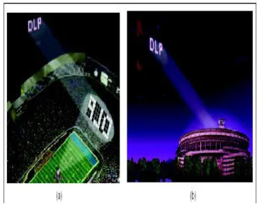
[image:2.612.361.544.396.543.2]Imagine that you are in a football stadium at night and it’s half-time. All the lights in the stadium are turned off; there is a blimp floating a few hundred feet above the field.
Figure 1. Fans in a stadium reflecting light toward a blimp
In figure 1(a) Light is projected from a spotlight toward fans in the stadium. When cued by a numbered signal, these fans hold up their reflective seat cushions and tilt them toward or away from a blimp. By doing so, the fans in the stadium are reflecting pixels of light toward the blimp. The result is that the light pattern created by the seat cushions projects an image onto the surface of the blimp. (b) A distant viewer sees the image on the blimp.
the spotlight reflects directly up to the blimp each time your number appears on the scoreboard screen. If your number is not displayed, you are to tilt the cushion away from the blimp and direct light down to the field. Each fan in the stands now controls a pixel of light. You can imagine that if some fans reflect the light toward the blimp, an image of some sort will appear on its side [Figure 1(a)].
Now imagine a viewer looking toward the stadium and the blimp from a remote distance [Figure 1(b)]. When looking at the blimp, he or she will see an image on the side of the blimp that is generated by the sports fans tilting their reflective seat cushions and reflecting light onto the side of the blimp.
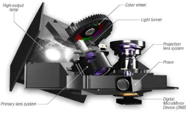
DLP technology accomplishes this same task, but it does so by processing light that is focused onto the DMD (Figure 2). At speeds greater than 1,000 times per second, the mirrors are electronically
[image:3.612.350.534.102.218.2]tilted. Light from a lamp is digitally reflected from the DMD, through a projection lens, and onto a screen. Colour is added through a colour wheel filter system.
Figure 2. DLP system operation
In much the same way the image was formed on the side of the blimp (figure 2(a)). DLP forms images for video. Shining light on the DMD and tilting the mirrors creates a digital image. Colour is added by placing a red, green, and blue colour wheel filter system in the optical path. As the wheel spins, the mirrors are tilted on for the exact amount of time required for each colour. At any given instant, only one of the primary light colour is hitting the DMD, but when the filter system spins fast enough, the colour blend to create a full-colour digital image. In figure 2(b), a viewer sees an image on the screen from a DLP projector.
V. DLPSTRUCTURE
A Digital Micro Mirror Device chip is the heart of Digital Light Processing projector, DMD can be described simply as a semiconductor light switch. The micro mirrors are mounted on the DMD chip and it tilts in response to an electrical signal. The tilt directs light toward the screen, or into a "light trap" that eliminates unwanted light when reproducing blacks and shadows. Other elements of a DLP projector include a light source, a
[image:3.612.67.272.294.491.2]colour filter system, a cooling system, illumination and projection optics.
Figure 3. DLP Projector internal structure
A DLP based projector system includes memory and signal processing to support a fully digital approach. Depending on the application, a DLP system will accept either a digital or analog signal. Analog signals are converted into digital in the DLPs front –end processing. Any interlaced video signal is converted into an entire picture frame video signal through interpolative processing. The signal goes through DLP video processing and becomes progressive Red (R), Green (G) and Blue (B) data. The progressive RGB data is then formatted into entire binary bit planes of data.
A. DMD Basic Principle
A DMD chip has on its surface several hundred thousand microscopic mirrors arranged in a rectangular array which correspond to the pixels in the image to be displayed. The mirrors can be individually rotated ±10-12°, to an on or off state. In the on state, light from the projector bulb is reflected into the lens making the pixel appear bright on the screen. In the off state, the light is directed elsewhere, making the pixel appear dark. To produce greyscales, the mirror is toggled on and off very quickly, and the ratio of on time to off time determines the shade produced. Contemporary DMD chips can produce up to 1024 shades of gray.
The mirrors themselves are made out of aluminium and are around 16 micrometres across. Each one is mounted on a yoke which in turn is connected to two support posts by compliant torsion hinges. In this type of hinge, the axle is fixed at both ends and literally twists in the middle. Tests have also shown that the hinges cannot be damaged by normal shock and vibration, since it is absorbed by the DMD superstructure.
The bias system is used because it reduces the voltage levels required to address the pixels such that they can be driven directly from the SRAM cell, and also because the bias voltage can be removed at the same time for the whole chip, so every mirror moves at the same instant.
B. DMD Modulator
The DMD chip is comprised of over one million mirrors. The size of each mirror is less than 1/5" the width of a human hair. The DMD is monolithically fabricated by Complementary Metal Oxide Semiconductor-like processes over a CMOS memory.
Figure 4. Isometric schematic of DMD pixels
Each light switch has an aluminum mirror, 16 µm² that can reflect light in one of two directions depending on the state of the underlying memory cell. Rotation of the mirror is accomplished through electrostatic attraction produced by voltage differences developed between the mirror and the underlying memory cell. With the memory cell in the on (1) state, the mirror rotates to +10°, with the memory cell in the off (0) state, the mirror rotates to -10°.
The mechanical portion of each pixel consists of a three layer structure. The centre layer, called beam layer, is suspended over the bottom electrode layer by thin torsion hinges. The top mirror layer is attached to the beam layer with a via post. The yoke may rotate about the torsion hinge axis to either side, landing on the electrode layer at specific tilt angles of +/- 10 degrees. Manipulation of the mirrors is accomplished electro statically utilizing the address electrodes on either side of the torsion hinge. These address electrodes are tied to the SRAM cell residing in the silicon backplane beneath each mirror structure. After passing through condensing optics and a colour filter system, the light from the projection lamp is directed at the DMD. When the mirrors are in ‘on’ position, they reflect light through the projection lens and onto the screen to form a digital, square-pixel projected image. Each mirror on the DMD array is electro statically tilted to the ‘on’ or ‘off’ positions. The technique that determines how long each mirror tilts in either direction is called pulse width modulation. The mirrors are capable of switching on and off more than 1000 times a second this rapid speed allows digital gray-scale and colour reproduction.
C. DMD Cell Structure
[image:4.612.352.544.237.436.2]The DMD pixel is a monolithically integrated MEMS superstructure cell fabricated over a CMOS SRAM cell. Figure 5 shows the pixel structure of in an exploded view illustrating how the various layers interrelate, including the underlying static random access memory (SRAM) cell that is used to address the pixel. An organic sacrificial layer is removed by plasma etching to produce air gaps between the metal layers of the superstructure. The air gaps free the structure to rotate about two compliant torsion hinges. The mirror is rigidly connected to an underlying yoke. The yoke, in turn, is connected by two thin, mechanically compliant torsion hinges to support posts that are attached to the underlying substrate. The address electrodes for the mirror and yoke are connected to the complementary sides of the underlying SRAM cell.
Figure 5. Pixel structure of a DMD cell
The yoke and mirror are connected to a bias bus fabricated at the metal-3 layer. The bias bus interconnects the yoke and mirrors of each pixel to a bond pad at the chip perimeter. The DMD mirrors are 16 µm² and made of aluminum for maximum reflectivity. They are arrayed on 17 µm centres to form a matrix having a high fill factor (~90%). The high fill factor produces high efficiency for light use at the pixel level and a seamless (pixilation-free) projected image
Electrostatic fields are developed between the mirror and its address electrode and the yoke and its address electrode, creating an efficient electrostatic torque. This torque works against the restoring torque of the hinges to produce mirror and yoke rotation in the positive or negative direction. The mirror and yoke rotate until the yoke comes to rest (or lands) against mechanical stops that are at the same potential as the yoke. Because geometry determines the rotation angle, as opposed to a balance of electrostatic torques employed in earlier analogy devices, the rotation angle is precisely determined.
ensuring that the projector's brightness uniformity and contrast ratio are not degraded.
Through the use of six photomask layers, the superstructure is formed with layers of aluminum for the address electrode (metal-3), hinge, yoke and mirror layers and hardened photo-resist for the sacrificial layers (spacer-1 and spacer-2) that form the two air gaps. The aluminum is sputter-deposited and plasma-etched using plasma-deposited SiO2 as the etch mask. Later in the packaging flow, the sacrificial layers are plasma-ashed to form the air gaps. The packaging flow begins with the wafers partially sawed along the chip scribe lines to a depth that will allow the chips to be easily broken apart later.
The partially sawed and cleaned wafers then proceed to a plasma etcher that is used to selectively strip the organic sacrificial layers from under the DMD mirror, yoke, and hinges. Following this process, a thin lubrication layer is deposited to prevent the landing tips of the yoke from adhering to the landing pads during operation. Before separating the chips from one another, each chip is tested for full electrical and optical functionality by a high-speed automated wafer tester.
D. Electronic Operation in DMD Cell
[image:5.612.346.544.222.339.2]The DMD pixel is inherently digital because of the way it is electronically driven. It is operated in an electrostatically bistable mode by the application of a bias voltage to the mirror to minimize the address voltage requirements. Thus, large rotation angles can be achieved with a conventional 5-volt CMOS address circuit. The organization of the DMD chip is shown in fig. Underlying each DMD mirror and mechanical superstructure cell is a six-transistor SRAM. Multiple data inputs and demultiplexers (1:16) are provided to match the frequency capability of the on-chip CMOS with the required video data rates. The pulse width modulation scheme for the DMD requires that the video field time be divided into binary time intervals or bit times. During each bit time, while the mirrors of the array are modulating light, the underlying memory array is refreshed or updated for the next bit time. Once the memory array has been updated, all the mirrors in the array are released simultaneously and allowed to move to their new address states.
Figure 6. Organisation of the DMD chip
This simultaneous update of all mirrors, when coupled with the PWM bit-splitting algorithm, produces an inherently low-flicker display. Flicker is the visual artifact that can be produced in CRTs as a result of brightness decay with time of the phosphor. Because CRTs are refreshed in an interlaced scan-line format, there is both a line-to-line temporal phase shift in brightness as well as an overall decay in brightness. DLP-based displays have inherently low flicker because all pixels are updated at the same time (there is no line-to-line temporal phase
shift) and because the PWM bit-splitting algorithm produces short-duration light pulses that are uniformly distributed throughout the video field time (no temporal decay in brightness).
VI. DIFFERENTCHIPMODELSOFDLP
Like digital video camcorders, DLP devices come in either one or three chip models. One chip DLP systems use a projection lamp to pass white light through a colour wheel that sends red-green-blue colours to the DMD chip in a sequential order to create an image on-screen. Only one DMD chip is used to process the primary red, green and blue colours.
Figure 7. Single Chip Model
In three chip DLP systems use a projection lamp to send white light through a prism, which creates separate red, green and blue light beams. Each beam is send to their respective red, green and blue DMD chip to process the image for display on-screen. One
chip models are said to produce a display of over 16-million colours. Three chip models can produce a display of over
35-trillion colours.
Figure8. Three Chip Model
[image:5.612.348.564.439.546.2] [image:5.612.75.262.515.621.2]Figure 9. Three closely spaced red, green, and blue LCD sub-pixels
LCDs are polarization-dependent, so one of the polarized light components in not used. This means that 50% of the lamp light never even gets to the LCD because it is filtered out by a polarizer. Other light is blocked by the transistors, gate and source lines in the LCD cell. In addition to light losses, the liquid crystal material itself absorbs a portion of the light. The result in that only a small amount of the incident light is transmitted through the LCD panel and on to the screen.
A. Amorphous Silicon LCD
Am-Si LCDs are built by depositing transistors on a large glass substrate. A transistor is located in the corner of each pixel while a thin conductive grid connects to each pixel on the panel. Pixels are made up of three individually controlled sub-pixel strips (red, green, and blue) to create a pixel capable of producing many colour combinations. Am-Si panels are used to create single-panel projectors, but these projectors suffer from poor image quality due to the side-by-side sub-pixel colour scheme.
B. Polycrystalline Silicon LCD
Polycrystalline silicon LCD, more commonly referred to as poly-Si, is a very popular LCD technology for projection display. These LCDs are fabricated at high temperatures on quartz substrates. Poly-Si LCD panels are much smaller than am-Si panels. They have smaller transistors and greater fill factors as well, but to date, poly-Si panels are monochromatic (meaning they don’t have the colour stripping found in am-Si panels). Colour is created in poly-Si projectors by using three separate LCD panels, beam-splitting mirrors, and a prism system. White light is split into red, green, and blue components. Each component of light is directed to its own LCD panel, where the light modulation occurs. The modulated light is then recombined by a prism so that the pixels from each panel are overlaid on each other to produce a colour image. The challenge for these three-panel poly-Si projectors is the precision alignment that is necessary to make the separate red, green, and blue image planes converge to produce a uniform, aligned picture.
C. Cathode Ray Tube Technology
Cathode ray tube technology is used in nearly all of today’s computer monitors and televisions. Electron beams are scanned back and forth and directed at a phosphor-emitting surface. When
[image:6.612.339.552.92.221.2]electrons hit this surface, light is emitted. By scanning the beams at rates faster than the eye can detect, a full image can be created.
Figure 10. The CRT Monitor
The problem with CRTs is that they are not digital but analogy displays. CRT technology probably will be replaced in the future by emerging LCD and DLP technology. In addition to being based on an old, analogy technology, CRTs also lack the brightness necessary for many larger screen applications. Further brightness limitations arise when CRT projection systems attempt to drive higher resolution video signals. The CRT’s brightness decreases as resolution increases, limiting the CRT’s potential as an optimal solution for HDTV. Because a CRT display system usually relies on three electron guns (Figure 10), one for each primary colour (red, green, blue), it also requires constant alignment and tweaking for optimum picture quality.
VIII. LCDVSDLPPROJECTOR
The gap between the mirrors in a DMD pixel (left) is smaller than the gap in an LCD display (right), resulting in a sharper display.
Figure 11. DMD Vs LCD
LCD projector tends to produce more saturated colour and sharper images. Depending on the resolution and size images may become pixilated. DLP Projectors typically offer deeper blacks and higher contrast. They may not project very detailed images well.
[image:6.612.336.551.453.568.2]Figure 12. Actual close-up photographs of both (a), an LCD-projected image, and (b), a DLP-LCD-projected image.
Projected images are produced by the combination of light shining through the LCD cells. LCDs have excellent colour saturation, usually have adjustable brightness and contrast, are typically brighter than DLPs at the same lumen output and have broader range of connectivity. Brighter, sharper, versatile, more reliable, consistent picture quality are the advantages of DLP.
IX. DMDTELEVISION
DLP (Digital Light Processing Television) is a technology that uses one, or sometimes three, electronic chips called Digital Micromirror Devices, or DMDs, to produce a vivid picture with a high contrast ratio on a high-definition large-screen TV. More than a million micromirrors mounted on the chip — five micromirrors, laid side by side, would fit across a human hair — respond to electric signals to focus the light from a white lamp either on, or away from, the TV screen. A one-chip DMD can produce more than 16 million colours when the light of each micromirror passes through a colour wheel; a three-chip DMD produces several trillion colours.
Figure 11. DLP Television
DLP was developed by Texas Instruments in the late 1980s, and at one time was used in thousands of theaters around the world. At home, DLP could strut its stuff best on large screens — from 43” to around 84”— which made it ideal for home theatres. DLPTs are frequently referred to as “projection” TVs, with rear-screen and front-screen projection models available. A 1080p DLPT has a resolution of 1,920x1, 080 pixels, and an aspect ratio of 16:9. A 65” screen can be viewed easily from a
distance of 5 yards.
DLPTs had several advantages over big-screen plasma and LCD TVs of the time:
1. They were more economical, inch per inch.
2. They were more svelte, being 13” to 15” slim and of a significantly lighter weight.
3. They were more reliable, simply because they had fewer parts vulnerable to failure. Lamp bulbs did need to be changed every 15 years or so.
4. They were immune to burn-in, which was caused by excessive gaming or by an ever-present logo in the corner of the screen.
Like its brethren the PC and the digital camera, each successive generation of DLPTs brought about an improved viewing experience by eliminating common causes for complaints. For example, speeding up the colour wheel banished the annoying “rainbows” on the screen, and the too-narrow viewing angle — 30 or 40 degrees, similar to that of a PC screen — was expanded to up to 180 degrees. That said, however, the Society of Motion Picture and Television Engineers did still recommend that viewers be within 30 degrees of the picture “cone” for optimal viewing.DLP televisions were eventually discontinued in 2012.
X. FUTUREUSESOFDLP
DLP has a number of potential uses beyond home theatre, television and film projection. DLP image projectors are becoming more common in business environments. Other applications that could incorporate its high-definition image creation are photo finishing, three-dimensional visual displays, holographic storage, microscopes, spectroscopes and medical imaging. A number of these technologies are already in development. Scientists and developers are likely to discover even more uses for DMDs and DLP technology in the future.
XI. ADVANTAGESOFDLP
1. Brighter.
DLP projectors are among the brightest available because DLP technology brings more light from lamp to screen, resulting in more effective presentation even when ambient light is difficult to control.
2. Sharper.
DLP projection’s unique technology comes closest to producing the exact mirror image of an incoming video or graphic signal, resulting in projection that’s seamless at any resolution.
3. Versatile.
[image:7.612.62.273.458.612.2]4. More reliable.
Display system using DLP technologies are able to recreate their incoming source material with each projection experience that will not fade over time.
5. Consistent picture quality.
A data projector based on DLP technology delivers knockout picture quality again and again because, being all-digital, recreates its image source every time of use. Unlike competing analogue technologies such as LCD, the semiconductor that makes DLP projection possible is virtually immune to heat, humidity vibration and other factors.
REFERENCES
[1] Digital Light Processing™: A New MEMS-Based Display Technology Larry J. Hornbeck Texas Instruments
[2] Emerging Digital Micromirror Device (DMD) Applications Dana Dudley, Walter Duncan, John Slaughter DLPTM Products New Applications Texas Instruments, Inc.
[3] P. Van Kessel, L. Hombeck, R. Meier and M. Douglass, “A MEMS-Based Projection Display,” Proc. IEEE, Vol. 86, No. 8, pp. 1687-1704, August, 1998.
[4] D.Doherty and G. Hewlett, “Pulse width modulation control in DLP Projectors,” July-Sept 98 Texas Instruments Technical Joumal, September 1998.
[5] V. Markandey, T. Clatanoff and G. Pettitt, “Video Processing for LPm Display Systems”, SPIE Image and Video Processing IV, San Jose, vol. 2666, pp. 21 - 32, January, 1996.
[6] E. Baumann, “The Fischer Large-Screen Projection System,” J. SMPTE, Vol. 60, pp. 344-356 (April 1953).
[7] R.J. Gove, “DMD Display Systems: The Impact of an All-Digital Display,” Society for Information Display International Symposium (June 1994). [8] L.J. Hornbeck and W.E. Nelson, “Bistable Deformable Mirror Device,”
OSA Technical Digest Series, Vol. 8, Spatial Light Modulators and Applications, p. 107 (1988).
[9] W.E. Nelson and L.J. Hornbeck, “Micromechanical Spatial Light Modulator for Electrophotographic Printers,” SPSE Fourth International Congress on Advances in Non-Impact Printing Technologies, p. 427 (March 20, 1988).
[10] L.J. Hornbeck, “Deformable-Mirror Spatial Light Modulators (Invited Paper),” Spatial Light Modulators and Applications III, SPIE Critical Reviews, Vol. 1150, pp. 86-102 (August 1989).
AUTHORS
First Author – Goldy Katal, B. Tech.(III Year), Department of
Electrical and Electronics Engineering, Maharaja Agrasen Institute of Technology, Delhi, Email: [email protected]
Second Author – Nelofar Tyagi, B. Tech.(III Year), Department
of Electronics and Communication Engineering, HMR Institute of Technology and Management, Delhi, Email:
Third Author – Ashish Joshi, B. Tech.(III Year), Department of
Electronics and Communication Engineering, HMR Institute of Technology and Management, Delhi, Email: