(
In this report:
Mechanical
Characteristics .. ,. ... -4
Functional Description of Interchange
Circuits ... ... -5
Electrical
Characteristics ... -10
Equalizers ... -13
Standard Interfaces for Selected
Configurations ... -14
DATAPRO
Data Networking 2744Standards
1
Electronic Industries
Association (EIA)
RS-449 Interface
Standard
Synopsis
Editor's Note
RS-449 defines the mechanical and electrical interface characteristics between data terminal equipment (DTE) and data circuit-terminating equipment (DCE). The electrical op-eration of the individual interchange circuits is specified in RS-422-A, for balanced operation, or in RS-423-A, for unbalanced operation. RS-449 permits greater cable distances, higher transmission speeds, and more interchange circuits than the older standard and is designed even-tually to replace EIA Standard RS-232-C.
The subject of this report is consid-ered as a mature standard. No signifi-cant developments are anticipated, but because of its importance in the industry, coverage is being continued.
-By Algis V. Salciunas Product Manager
Report Highlights
In 1977, the Electronic Industries Association (EIA) developed the RS-449 Standard, General Purpose 37-Position and 9-37-Position Interface for Data Terminal Equipment and Data Circuit-Terminating Equipment Em-ploying Serial Binary Data Inter-change.
Developed in cooperation with the standards activities of the Interna-tional Organization for Standardiza-tion (ISO) and the InternaStandardiza-tional Consultative Committee on Telegra-phy and Telephony (CCITT), RS-449 is compatible with ISO 4902 and CCITT V.24. An addendum, RS-449-1, issued in February 1980, out-lined supplemental changes to Circuit NS (New Signal).
Copies of RS-449 can be obtained from the Electronic Industries Asso-ciation, 2001 I Street NW, Washing-ton, DC 20006. Copies of EIA Standards RS-422-A and RS-423-A are also available.
@ 1991 McGraw·HIII, Incorporated. Reproduction Prohib~ed. Datapro Information Services Group. Delran NJ 08075 USA
2 2744
Standards
Analysis
The RS-449 Standard was intended to replace the familiar RS-232-C standard. RS-449 and its com-panion standards were developed to permit an or-derly transition from existing equipment using RS-232-C to a newer generation of equipment using RS-449, without forcing obsolescence or costly ret-rofits. Most U.S. manufacturers of data communi-cations equipment, however, have embraced the older standard, and RS-232-C remains the more common interface.
RS-449 operates in conjunction with either of two standards specifying electrical characteristics: RS-422-A, for balanced circuits; and RS-423-A, for unbalanced circuits. When each interface circuit has its own ground lead, the circuit is balanced. When an interface uses a common or shared grounding technique, it is unbalanced.
RS-449 governs the mechanical and electrical characteristics of the interface between data termi-nal equipment (DTE) and data circuit-terminating equipment (DCE). As they relate to this standard, DTE is the hardware on the business machine side of the interface (e.g., teleprinters, CRTs; PEPs, CPUs, etc.), and DCE is the modem, signal con-verter, or other device between the DTE and the communications line. RS-449 applies to binary, serial, synchronous, or asynchronous communica-tions. Half- and full-duplex modes are accommo-dated, and transmis~ion can be point-to-point or multipoint over two- or four-wire facilities. Point-to-point arrangements may be either switched or dedicated. Multipoint arrangements are connected by dedicated lines.
An RS·449/RS·232·C Comparison
RS-232-C defines 22 specific functions; RS·449 defines 30 functions that supplement some of the limitations of RS-232-C. Compatibility between RS-232-C and RS-449 can be accomplished with an interface converter. The additional functions provided by RS-449, however, are unavailable once it has been converted for compatibility with RS-232-C. A maximum data transfer rate of 20K
MAY 1991
Electronic Industrle. AlI_elation (EIA) RS ... Interface Standard
Data Networking
bps and a distance limitation of 15 meters (50 feet) are recommended when an interface converter is used.
Most of the interchange functional definitions given in RS-232-C have been retained in RS-449; some significant differences follow:
• Data rates are accommodated up to 2M bps when using the balanced interface specified in RS-422-A.
• RS-449 specifies a different interface connector size and latching arrangement. A 37-pin connec-tor is used to accommodate additional interface leads that support newly defined functions and also to accommodate balanced operation (when used) for 10 interchange circuits. In addition, a separate 9-pin connector is specified to serve secondary channel interchange circuits, when applicable.
• Ten additional circuit functions are defined: three circuits for control and status of test func-tions associated with DCE; two circuits for con-trol and status of a transfer function of the DCE to a standby channel; one circuit to provide an out-of-service function under control of the DTE; one circuit to provide a New Signal func-tion; one circuit to provide DCE frequency se-lection; and two circuits to provide a common reference for each direction of transmission across the interface.
• Three interchange circuits defined in RS-232-C have not been included in RS-449. Pins 9 and 10 of RS-232-C are reserved for data set testing; these have been excluded in RS-449 to mini-mize interface connector size. ·Protective ground (RS-232-C Circuit AA) has also been excluded so that bonding of equipment frames may be implemented in accordance with na-tional and local electrical codes.
• The option in RS-232-C that permits the omis-sion of the Request to Send interchange circuit for certain transmit-only or full-duplex applica-tions is excluded in RS-449.
• The definition of the Data Set Ready function in RS-232-C has been changed in RS-449, and a new function, Data Mode, which indicates fur-ther DCE status conditions, was added.
• To avoid confusion with RS-232-C, RS-449 has established its own set of circuit names and mnemonics.
(
Data Networking Electronic Industries As.oclatlon (EIAI RS·449 Interface Standard
2744
Standards
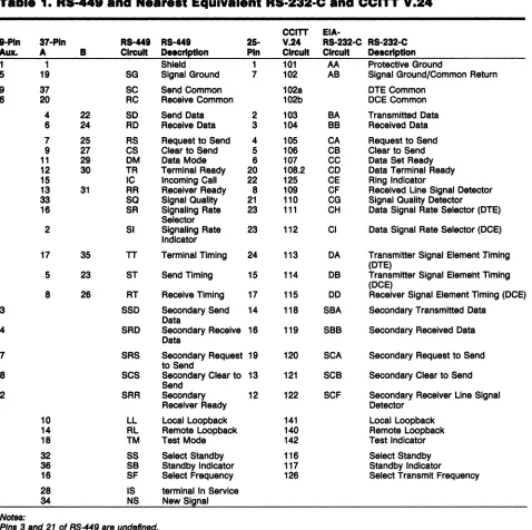
[image:3.612.58.536.92.568.2]3
Table 1.
RS·44.
and Nea,.st EquivalentRS·232·C
andCCITT V.24
CCtTT
EtA-t-Pln 37-Pln RS-448 AS-449 25- V.24 AS-232-C AS-232-C
Au .. A B Circuit Deecrlptlon Pin Circuit Circuit De.crlption
1 1 Shield 1 101 AA Protective Ground
5 19 SG Signal Ground 7 102 AB Signal Ground/Common Return
9 37 SC Send Common 102a DTECommon
6 20 RC Receive Common 102b DCE Common
4 22 SO Send Data 2 103 BA Transmitted Data
6 24 RD Receive Data 3 104 BB Received Data
7 25 RS Request to Send 4 105 CA Request to Send
9 27 CS Clear to Send 5 106 CB Clear to Send
11 29 OM Data Mode 6 107 CC Data Set Ready
12 30 TR Terminal Ready 20 108.2 CD Data Terminal Ready
15 IC Incoming Call 22 125 CE Ring Indicator
13 31 RR Receiver Ready 8 109 CF Received Une Signal Detector
33 SQ Signal Quality 21 110 CG Signal Quality Detector
16 SR Signaling Rate 23 111 CH Data Signal Rate Selector (DTE)
Selector
2 SI Signaling Rate 23 112 CI Data Signal Rate Selector (DCE)
Indicator
17 35 TT Terminal Timing 24 113 DA Transmitter Signal Element Timing
(DTE)
5 23 ST Send Timing 15 114 DB Transmitter Signal Element Timing
(DCE)
8 26 RT Receive Timing 17 115 DO Receiver Signal Element Timing (DCE)
3 SSD Secondary Send 14 118 SBA Secondary Transmitted Data
Data
4 SRD Secondary Receive 16 119 SBB Secondary Received Data
Data
7 SRS Secondary Request 19 120 SCA Secondary Request to Send
to Send
8 SCS Secondary Clear to 13 121 SCB Secondary Clear to Send
Send
2 SRR Secondary 12 122 SCF Secondary Receiver Une Signal
Receiver Ready Detector
10 LL Local Loopback 141 Local Loopback
14 RL Remote Loopback 140 Remote Loopback
18 TM Test Mode 142 Test Indicator
32 SS Select Standby 116 Select Standby
36 SB Standby Indicator 117 Standby Indicator
16 SF Select Frequency 126 Select Transmit Frequency
28 IS terminal In Service
34 NS New Sisnal
Notes:
PI". 3 and 21 of RS-449 are undefined. 37-pln designation B - return.
Table 1 presents the RS-449 pin connection assign- particular function. The CCITT chose to assign ments as they relate to the RS-232-C and V.24 as- coded characters to each function instead of
indi-signments. vidual circuits. This character-oriented control
procedure has two significant advantages: An al-An RS-449/CCITT X.21 Comparison most unlimited number of functions can be as-RS-449 and CCITT X.21 were designed to expand signed (over 100 functions per lead), creating more the capabilities of RS-232-C and CCITT V.24. terminal-to-network control and providing for fu-While both standards organizations set out to at- ture expansion; and a smaller (IS-pin) interface tain the same goal, different methodologies were connector can be used, reducing both the complex-used to design the newer interfaces. The EIA chose ity of the circuitry involved and, presumably, the to base its RS-449 Standard on the same philoso- problems associated with a larger connector. phy as ~S-232-C, namely, assigning each circuit a
@ 1991 McGraw-Hili. Incorporated. Reproduction Prohibited. MAY 1991
4 2744
Standards
While RS-449 places the transmission speed and distance limitations between the terminal and the network at 2M bps and 60 meters, X.21 is op-erable up to 10M bps over distances up to 1,000 meters. Also, CCITT X.21 permits more effective use of switched network services, since the data call interface, EIA RS-366-A, necessary for RS-449 signal establishment, is not required. This is im-portant because it eliminates the need for dedi-cated facilities in order to achieve an acceptable response time.
Federa. Standard 1031
Federal Standard 1031 FS-1031 provides for three variations of RS-449. It was adopted for use by all federal agencies in the design and procurement of DTEs and DCEs used for data communications. Two related standards, FS-I030 and FS-I020, cor-respond to RS-423-A and RS-422-A, respectively, for unbalanced and balanced electrical circuits.
The varieties of RS-449 provided by FS-I031 include:
• An 449 interface interoperable with RS-232-C.
• An RS-449 interface interoperable with the MIL standards used by the federal government.
• An RS-449 interface not requiring interopera-bility with RS-232-C.
Due to the fact that only 10 of the interchange cir-cuits defined in RS-449 are required, it is possible for two devices conforming to the RS-449 interface under two different federal standards to be incom-patible. In fact, because only these 10 circuits must be defined, potentially, any RS-449 implementa-tion may be incompatible with any other.
Mechanical Characteristics
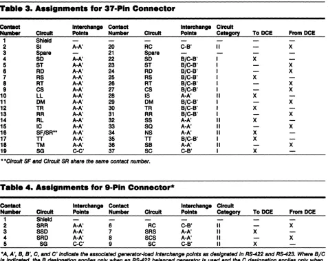
The point of demarcation between the DTE and the DCE is located at connector plugs on the DCE or at an interface point no further than 10 feet from the DCE. A 37 -pin connector is specified for all interchange circuits with the exception of sec-ondary channel circuits, which are accommodated in a separate 9-pin connector. The nine-pin con-nector is implemented only when the secondary channel is used. These connectors are from the same family as those used in RS-232-C applica-tions.
MAY 1991
Electronic Industries Data Networking Association (EIA)
RS-448 Interface Standard
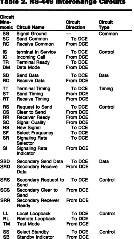
Table
2.
RS-448 Interchang. CircuitsCircuit
Mne- Circuit Circuit
monic Circuit Name Direction Type
SG Signal Ground Common
SC Send Common ToDCE
RC Receive Common From DCE
IS terminal In Service ToDCE Control IC Incoming Call From DCE
TR Terminal Ready ToDCE OM Data Mode From DCE
SO Send Data ToDCE Data
RD Receive Data From DCE
TT Terminal Timing ToDCE Timing ST Send Timing From DCE
RT Receive Timing From DCE
RS Request to Send ToDCE Control
CS Clear to Send From DCE RR Receiver Ready From DCE
sa
Signal Quality From DCENS New Signal ToDCE
SF Select Frequency ToDCE SR Signaling Rate ToDCE
Selector
SI Signaling Rate From DCE Indicator
SSD Secondary Send Data ToDCE Data SRD Secondary Receive From DCE
Data
SRS Secondary Request to ToDCE Control Send
SCS Secondary Clear to From DCE Send
SRR Secondary Receiver From DCE Ready
LL Local Loopback ToDCE Control RL Remote Loopback ToDCE
TM Test Mode From DCE
SS Select Standby ToDCE Control
se
Standby Indicator From DCEThe 37-pin connector is arranged with 19 pins on the top row and 18 pins on the bottom row. The nine-pin connector is arranged with five pins on the top row and four pins on the bottom row. Pin positions are staggered to prevent im-proper connection. In all cases, the DTE provides the cable run (minimum of 200 feet when using RS-422-A or RS-423-A interchange circuits) termi-nated in a male connector.
The DCE is equipped with a female connec-tor. The connectors are equipped with a latching block that permits latching and unlatching without the need for a tool. The latching block also permits the use of screws to fasten the connectors together.
Intermediate equipment, such as the passive adapter used in RS-232-C-to-RS-449 connections, is placed in series with the two units such that the
@ 1991 McGraw-Hili. Incorporated. Reproduction Prohibited. Datapro Information Services Group. Delran NJ 08075 USA
[image:4.612.322.555.71.485.2]Data Networking Electronic Indu.trle. Anoelatlon lElA) RS ... Intertaee Standard
cable from the DTE plugs into a female connector on the intermediate equipment; the intermediate equipment presents a DTE (male) interface toward the DCE.
Functional Description of Interchange Circuils
Interchange circuits fall into four general classifica-tions: ground (or common return), data circuits, timing circuits, and control circuits. A list of RS-449 interchange circuits showing mnemonic name, circuit identification, circuit direction, and circuit type is presented in Table 2. The connector pin assignments as compared to the functional inter-change circuits are given in Table 1, along with an equivalency table, showing the nearest equivalent RS-232-C and CCITT V.24 functions in relation to each RS-449 function. A functional description of each of the RS-449 interchange circuits follows.
Ground or Common Return Circuits
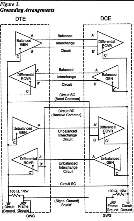
Circuit SG (Signal Ground) is connected directly to the DTE circuit ground (circuit common) and pro-vides a conductive route between the DTE and DCE signal commons. See Figure 3 for grounding arrangements.
Circuit SC (Send Common) is connected to the DTE circuit ground (circuit common) for use at the DCE as a reference potential for Category II interchange circuit receivers.
Circuit RC (Receive Common) is connected to the DCE circuit ground (circuit common) for use at the DTE as a reference potential for Category II interchange circuit receivers.
Data Circuits
Circuit SD (Send Data) transfers the data signals originated by the DTE to the DCE. The DTE holds Circuit SD in the binary "one" (marking) condi-tion unless an ON condicondi-tion is present on follow-ing circuits: RS (Request to Send); CS (Clear to Send); DM (Data Mode); and when implemented, TR (Terminal Ready) and IS (terminal In Service). The DCE disregards any signal appearing on Cir-cuit SD when an OFF condition exists on one or more of these circuits. All data signals transmitted across the interface on Circuit SD while an ON condition is maintained on each of these circuits are transmitted by the DCE to the communications channel.
@ 1991 McGraw-Hili, Incorporated. Reproduction Prohibited. Datapro Information Services Group. Delran NJ 08075 USA
2744
Standards
5
Circuit RD (Receive Data) transfers data sig-nals generated by the DCE to the DTE in response to line signals received from a remote station. Cir-cuit RD is held in the binary "one" (marking) con-dition while Circuit RR (Receiver Ready) is in the OFF condition. On half-duplex channels, Circuit RD is held in the marking condition when Circuit RS is ON and for a brief interval when Circuit RS makes the transition from ON to OFF. This allows for the completion of the transmission and for the decay of channel reflections.
Circuit SSD (Secondary Send Data) is the sec-ondary channel's equivalent to Circuit SD. The DTE generates and signals on this circuit and transfers the signals to the local secondary channel transmitter for transmission to one or more remote stations. The DTE holds Circuit SSD in the mark-ing condition unless an ON condition is present on each of the following circuits: SRS (Secondary Re-quest to Send); SCS (Secondary Clear to Send); DM (Data Mode); and when implemented, TR (Terminal Ready); and IS (terminal In Service). The DCE disregards each signal appearing on Cir-cuit SSD if an OFF condition exists on one or more of these circuits. All signals transmitted across the interface on Circuit SSD when the stated conditions are satisfied, are transmitted by the DCE to the communications channel.
If the secondary channel is used only for cir-cuit assurance or to interrupt data transmission in the primary channel (less than 10 bps capability), Circuit SSD is not usually provided. In this case, the secondary channel carrier is turned ON and OFF by Circuit SRS. An interrupt condition is in-terpreted when a carrier OFF condition exists.
Circuit SRD (Secondary Receive Data) is the secondary channel's equivalent of Circuit RD. If the secondary channel is used only for circuit as-surance or to interrupt data transmission in the primary channel, Circuit SRD is not usually pro-vided. See Circuit SRR (Secondary Receiver Ready).
Timing Circuits
Circuit IT {Terminal Timing) provides the DCE with the signal element timing for transmitting from the DTE. The ON to OFF transition indi-cates the center of each signal element on Circuit SD. When Circuit IT is implemented, the DTE provides timing information on this circuit when the power ON condition exists. The DTE may
8 2744 Electronic Industries Association (EIAI Data Networking
Standards 118-448 Interface
[image:6.612.76.553.62.442.2]Standard
Table 3. assignments for 37·Pln Connector
Contact Interchange Contact Interchange Circuit
Number Circuit PoInts Number Circuit Points Category ToDCE From DCE
1 Shield
2 SI A-A' 20 RC e-B' II X
3 Spare 21 Spare
4 SO A-A' 22 SO B/e-B' I X
5 ST A-A' 23 ST B/e-B' I X
8 RO A-A' 24 RO S/e-B' I X
7 RS A-A' 25 RS B/e-B' I X
8 RT A-A' 28 RT B/e-B' I X
9 CS A-A' 27 CS B/e-B' I X
10 LL A-A' 28 IS A-A' II X
11 OM A-A' 29 OM B/C-B' I X
12 TR A-A' 30 TR B/e-B' I X
13 RR A-A' 31 RR B/e-B' I X
14 RL A-A' 32 SS A-A' II X
15 IC A-A' 33
sa
A-A' II X18 SF/SR** A-A' 34 NS A-A' II X
17 TT A-A' 35 TT B/e-B' I X
18 TM A-A' 36 SB A-A' II X
19 SG C-C' 37 SC CoB' I X
* *Clrcult SF and Circuit SR share the same contact number.
Table 4. assignments for 9-Pln Connector·
Contact Interchange Contllct Interchange Circuit
Number Circuit Points Number CIrcuit Points Category ToDCE From DCE
1 Shield
2 SRR A-A' 6 RC CoB' II X
3 SSO A-A' 7 SRS A-A' II X
4 SRO A-A' 8 SCS A-A' II X
5 SG C-C' 9 SC CoB' II X
*A, A', 8, 8', C, and C' Indicate the 88soc/ated generator-load Interchange points 88 d88lgnated In RS-422 and RS-423. Where 8/C
Is Indicated, the 8 designation applies only when an RS-422 balanced generator Is used and the C designation applies only when an RS-423 unbalanced generator Is uaed. The 8'Iead of circuits IS, NS, SF/SR, LL, RL, SS, SSD, and SRS Is Internally connected
within the DCE to Circuit SC. The 8' lead of Circuits IC, SQ, SI, TM, S8, SRD, SCS, and SRR Is Internally connected within the DTE to Circuit Re.
withhold timing infonilation for short periods pro-vided that Circuit RS is OFF, for example, during DTE testing.
Circuit ST (Send Timing) provides the DTE with signal element timing information for trans-mitting from the DCE. The DTE provides a data signal on Circuit SD. Transitions between the sig-nals are concurrent with the ON/OFF transitions on Circuit ST.
Circuit RT (Receive Timing) provides the DTE with signal element timing received from the DCE. The transition from ON to OFF indicates the center of each signal element on Circuit RD. The DCE provides timing information on this cir-cuit when the DCE is powered ON. The DCE may withhold timing information on this circuit and Circuit ST for short periods provided that Circuit DM (Data Mode) is OFF.
MAYf9IJ1
Control Circuits
Circuit IS (terminal In Service) indicates whether the DTE is available for service. The ON condition indicates that the DTE is available and, in
switched networks that use line hunting, allows incoming calls to be connected to the DCE. The OFF condition indicates that the DTE is unavail-able for service. In switched applications using line hunting, the OFF condition causes the DCE to ap-pear busy so that an incoming call will skip over the DCE in the hunting process. Any DTE out-of-service condition initiates the OFF condition.
Circuit IC (Incoming Call) indicates to the DTE that an incoming call is being received by the DeE. The ON condition indicates that an incom- . ing call is being received. The ON condition ap-pears with the ON segment of the ring cycle (during rings) on the channel. The OFF condition is maintained during the OFF segment of the ring
(
Data Networking Electronic Industries Association IEIAI RS·448 Interface Standard
cycle (between rings) and at any time when ringing is not being received. The OFF condition of Cir-cuit TR does not disable the operation of CirCir-cuit
Ie.
Circuit TR (Terminal Ready) controls DCE switching to and from the communications chan-nel. The ON condition prepares the DCE for con-nection to a communications channel and maintains the connection. Ifthe station is equipped for automatic answering, connection to the line occurs in response to a combination of the ring signal and an ON condition of Circuit TR. Usually the DTE may present an ON condition over Circuit TR when it is ready to transmit or re-ceive data; except when Circuit TR is turned OFF, it may not be turned ON again until Circuit DM (Data Mode) is turned OFF by the DCE. The OFF condition of Circuit TR removes the DCE from the communications channel only after all data presented before TR was turned OFF have been transferred to the DTE. The OFF condition ofTR does not disable the operation of Circuit IC (In-coming Call).
Circuit DM (Data Mode) indicates the status of the local DCE. The ON condition of this circuit indicates that the DCE is in the data transfer mode: A condition in which the local DCE is con-nected to a communications channel, is not in al-ternate voice or dial mode, and has completed any timing functions required to complete call estab-lishment, including the transmission of any re-quired answer tone.
When the local DCE does not transmit an answer tone, or when the duration of the answer tone is controlled by the remote DCE, the ON con-dition is presented as soon as all the concon-ditions listed above are satisfied. This circuit is used to indicate only the status of the local DCE; the ON condition does not indicate the establishment of a communications channel or the status of remote station equipment.
The OFF condition is present at all other times and indicates to the DTE that it should disre-gard signals appearing on all other interchange cir-cuits, with the exception of Circuit IC (Incoming Call), Circuit TM (Test Mode), and Circuit SB (Standby Indicator). Circuit IC is not impaired by the OFF condition. When the OFF condition oc-curs during the progress of a call before Circuit TR (Terminal Ready) is turned OFF, the DTE inter-prets this as a lost or aborted connection and takes
@ 1991 McGraw-Hili, Incorporated. Reproduction Prohibited. Datapro Information Servicas Group. Delran NJ 08075 USA
2744 Standards
7
action to terminate the call. Any subsequent ON condition on Circuit DM is considered to be a new call.
When Automatic Calling Equipment (ACE) is used in conjunction with the DCE, the OFF to ON transition of Circuit DM is not an indication that the ACE has relinquished control of the communi-cations channel. This indication is given on the appropriate circuit in the ACE interface as per EIA Standard RS-366-A.
Circuit DM is in the OFF condition for DCE tests that are not conducted through the DTE/DCE interface. Circuit DM responds normally, if it is not clamped OFF for tests conducted through the DTElDCE interface.
Circuit RS (Request to Send) controls the transmit function of the local DCE and, on half-duplex channels, the direction of data transmis-sion. On one-way-only (duplex) channels, the ON condition holds the DCE in the transmit mode; the OFF condition suppresses transmission. On a half-duplex channel, the ON condition holds the DCE in the transmit mode and suppresses the receive mode. The OFF condition holds the DCE in the receive mode.
The DCE is instructed to enter the transmit mode by a transition from OFF to ON. The DCE responds by taking any necessary action and indi-cates completion of such action by turning ON Cir-cuit CS (Clear to Send), thereby permitting the DTE to transfer data across Circuit SD. A transi-tion from ON to OFF instructs the DCE to com-plete transmission of all data previously
transferred and then to assume a nontransmit, or receive mode, as appropriate. The DCE responds to this instruction by turning OFF Circuit CS.
When Circuit RS is turned OFF, it is not turned ON again until Circuit CS has been turned OFF by the DCE. An ON condition is required on Circuit RS as well as on Circuits CS; DM; and, where implemented, TR and IS, whenever data is transferred across the interface on Circuit SD by the DTE. Circuit RS may be turned ON at any time when Circuit CS is OFF, regardless of the sta-tus of any other interface circuit.
Circuit CS (Clear to Send) is used to indicate that the DCE has been conditioned to transmit data over the communications channel. The ON condition, together with the ON on Circuits RS; DM; and, where implemented, TR and IS, indi-cates to the DTE that signals on Circuit SD will be
8 2744
Standards
Electronic Indu ... Auoclallon (EIA)
U ... Interface Stllndard
Data Networking
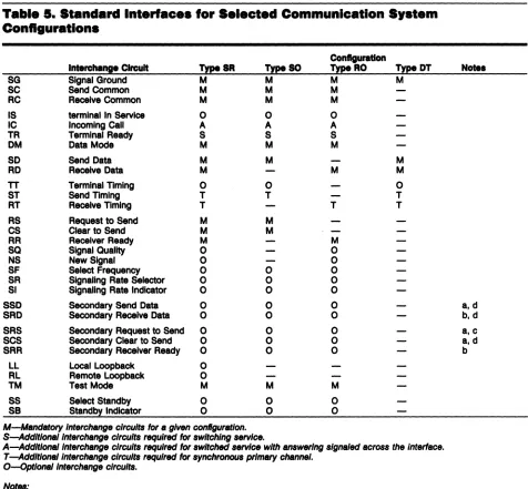
Table
a.
Standard Interfaces for S.lected Communication System
Configurations
Configuration
Interchll!!l! CIrcuit TypeSR Type 80 TypeRO Type DT
SG Signal Ground M M M M
SC Send Common M M M
RC Receive Common M M M
IS terminal In Service 0 0 0
IC Incoming Call A A A
TR Terminal Ready S S S
OM Data Mode M M M
SO Send Data M M M
RD Receive Data M M M
TT Terminal TIming 0 0 0
ST Send Timing T T T
RT Receive Timing T T T
RS Request to Send M M
CS Clear to Send M M
RR Receiver Ready M M
sa
Signal Quality 0 0NS New Signal 0 0
SF Select Frequency 0 0 0
SR Signaling Rate Selector 0 0 0
SI Signaling Rate Indicator 0 0 0
SSD Secondary Send Data 0 0 0 a,d
SRD Secondary Receive Data 0 0 0 b,d
SRS Secondary Request to Send 0 0 0 a, c
SCS Secondary Clear to Send 0 0 0 a,d
SRR Secondary Receiver Ready 0 0 0 b
LL Local Loopback 0
RL Remota Loopback 0
TM Test Mode M M M
SS Select Standby 0 0 0
sa
Standby Indicator 0 0 0M-MlJIIdatory Interchange circuits for a given configuration. S-AddltJonaIlnterchange circuits required for switching service.
A-Addltlonallnterchange circuits required for switched service with answering signaled across the Interface. T -Additional Interchange circuits required for .ynchr0n0u8 prlmary chennel.
O-optlonal Interchange circuits.
Notes:
.-Unnecessary " secondary channel Is receive only. b-Unnecessary " .econdary channell. transmit only.
c-Unnecessary " secondary channel Is a backward channel.
d-Unnecessary " .econdary channell. usable only for circuit ... urance or to Interrupt the flow of date In the primary channel.
transmitted to the data channel. The OFF condi-tion indicates that the DTE should not transfer data across the interface. The ON condition of Cir-cuit CS is a response to the occurrence of concur-rent ON conditions on Circuits DM and RS, delayed as appropriate, to allow the establishment of a communications channel.
Circuit RL (Remote LoopbackJ is used to con-trol the remote loopback test function (see Figure 1). The ON condition of this circuit causes the lo-cal DCE to signal the initiation of the RL test to
MAY 1991
the remote DCB. After turning RL ON and detect-ing an ON condition on the Test Mode (TM) cir-cuit, the local DTE can operate in a duplex mode using the circuitry of the local and remote DCEs. An OFF condition causes the RL condition to be released. Test condition RL causes communica-tions to be out-of-service to the remote DTE. WhenRL is activated, the DCE using the RL pre-sents an OFF condition on Circuit DM and an ON condition on Circuit TM to the DTE. The local DCE presents an ON condition on Circuit TM and allows Circuit DM to respond normally.
@ 1991 McGraw-Hili, Incorporated. Reproduction Prohibited.
[image:8.612.72.548.63.504.2]rf
\
(
Data Networking
:
Local Local
OTE DeE
Electronic Indu.trle. A . . oclldlon IEIAI RS-44' Interrace Standard
FaciUty Test
Center
"
\\ \
\ \
\ \
\ \
LL)I
,•
\..
.'
Circuit TM (Test Mode) indicates that local DCE is in test condition. ON indicates a test con-dition and OFF indicates normal operation. When testing (either LL or RL) is conducted through the local DTE/DCE interface, Circuit DM responds normally; when testing is not conducted through this interface, Circuit DM is held in an OFF condi-tion.
Circuit SS (Select Standby) is used to select normal communications facilities (OFF) or standby facilities (ON).
Circuit SB (Standby Indicator) indicates that the DCE is operating over normal communications facilities (OFF), or standby facilities (ON).
Circuit SI (Signaling Rate Indicator) is used to indicate which of two signaling rates is in use when employing a dual-rate, synchronous DCE or which of two ranges is in use for a dual-range, asynchronous DCE. The ON condition indicates the high rate or range of rates; an OFF indicates that the lower is in use. If included in the interface, timing signal rates are controlled by this circuit.
Circuit SRS (Secondary Request to Send) is functionally equivalent to Circuit RS and is used to control the secondary channel transmitter. When the secondary channel is used only for circuit as-surance or to interrupt data transmission in the primary channel, Circuit SRS can be used to tum ON the secondary channel unmodulated carrier. The OFF condition of this circuit turns OFF the secondary channel carrier and signals an interrupt condition to the remote end of the channel.
Circuit SCS (Secondary Clear to Send) is functionally equivalent to Circuit CS; it is used to indicate that the DCE is conditioned to transmit data on the secondary channel. Circuit SCS is not used when the secondary channel is used only for circuit assurance or as an interrupt channel.
Circuit SRR (Secondary Receiver Ready) is functionally equivalent to Circuit RR; it indicates
@ 1991 McGraw-Hili, Incorporated. Reproduction Prohibited. Datepro Information Services Group. Delran NJ 08075 USA
2744
Standards
Figure 1.
LooplKu:le Tats
Local loopback and remote loopback tests as seen from the local DTE.
•
that a proper signal is being received by the ondary channel receiver in the DCE. When the sec-ondary channel is used only for circuit assurance or as an interrupt channel, Circuit SRR is used to in-dicate channel status or to signal an interrupt. An ON condition indicates circuit assurance; an OFF indicates circuit failure.
Circuit LL (Local Loopback) is used to con-trol the localloopback test condition in the local DCE. See Figure 1. The ON condition instructs the DCE to transfer its output to its receive signal con-verter to check local operation. After establishing the LL test condition, the local DTE turns ON Cir-cuit TM. Once TM is ON, the DTE may operate in a duplex mode and may use all the circuits in the interface. The OFF causes the DCE to release the LL test condition. The LL test does not disable Cir-cuit Ie.
Circuit NS (New Signal) is used by the DCE to accelerate the acquisition of a new line signal in multipoint networks. Two methods of operation are defined in RS-449 (Circuit NS must remain OFF at all other times). The first method is where Circuit RR is ON when Circuit NS is activated. In this case, the DCE is instructed by the ON condi-tion of Circuit NS to detect the disappearance of the line signal and to place Circuit RD in the mark-ing condition. When the received line signal falls below the threshold of the received line signal de-tector, the DCE turns Circuit RR OFF and pre-pares to detect the appearance of a new signal. Circuit NS may be turned OFF after one unit inter-val and must be turned OFF after Circuit RR is turned OFF.
The second method occurs when Circuit RR is turned OFF while Circuit NS is turned ON. In this case, the ON condition of Circuit NS instructs the DCE to prepare itself to detect the appearance of a new line signal. Circuit NS may then be turned
10 2744
Standards
OFF after a one-unit interval and must be turned OFF before the new line signal is expected.
Circuit RR (Receiver Ready) indicates that the DCE is conditioned to receive signals from the data channel. The ON condition indicates that the DCE is receiving a signal that meets its criteria, which are established by the DCE manufacturer. The OFF condition causes Circuit RD to be clamped to the marking condition. On half-duplex channels, Circuit RR is OFF whenever Circuit RS is in the ON condition and for a brief interval fol-lowing the ON to OFF transition of Circuit RS (see Circuit RD).
Circuit SQ (Signal Quality) indicates a rea-sonable probability of error in the received data. An ON condition is held as long as no indication of an error has occurred. An OFF condition indicates a high probability of error; the error criteria are established by the DCE manufacturer.
Circuit SF (Select Frequency) is used by the DTE to select the transmit and receive frequencies of the DCE. The ON condition selects the higher frequency band for transmission and the lower band for reception. The OFF condition selects the reverse.
Circuit SR (Signaling Rate Selector) ON/OFF transitions are used to select one of two signaling rates of a dual-rate, synchronous DCE or to select one of two ranges of signaling rates of a dual-range, asynchronous DCE. The ON condition selects the higher rate or range of rates; the OFF condition selects the lower. If included in the interface, the rate of timing signals is controlled by this circuit.
Electrical Characteristics
The electrical characteristics ofthe individual in-terchange circuits are specified in RS-422-A for balanced operation and in RS-423-A for unbal-anced operation. RS-449 specifies the mechanical configuration of the connector and the pin assign-ments and functions of the entire interface, includ-ing the timinclud-ing and interrelationships Of the various circuits.
Compatibility with RS-232-C equipment can be achieved by modifications to the RS-449 hard-ware, which may include the placement of an adapter in series between the DTE and DCE faces. The adapter is passive and serves to inter-connect the 37-pin and 9-pin, when used,
connector(s) with the RS-232-C 25-pin connector.
MAY 1991
~Iclndu.~ •• u-Iatlon IliA)
R ... lnt.rfac • • hlndarel
Data Networking
It also provides signal compatibility between the devices. RS-232-C calls for between +3 and +25 volts for a space or ON (binary "zero"), and be-tween -3 and -25 volts for a mark or OFF (binary "one"); RS-449 specifies between + 200 millivolts and +6 volts for a space or ON (binary "zero"), and between - 200 millivolts and - 6 volts for a mark or OFF (binary "one").
To assign electrical characteristics to the in-terchange circuits, defined functionally, earlier in this report, RS-449 has defined two separate cate-gories of circuits. Category 1 Circuits are as follows:
• Circuit SD (Send Data)
• Circuit RD (Receive Data)
• Circuit TT (Terminal Timing)
• Circuit ST (Send Timing)
• Circuit RT (Receive Timing)
• Circuit RS (Request to Send)
• Circuit CS (Clear to Send)
• Circuit RR (Receiver Ready)
• Circuit TR (Terminal Ready)
• Circuit DM (Data Mode)
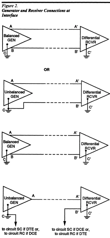
For applications where the data signaling rates of Circuits SD and RD are 20K bps or less, the indi-vidual Category I circuits can be arranged as per RS-442-A (balanced) or as per RS-423-A (unbal-anced), or any combination thereof. Two leads are brought out to the interface connector to intercon-nect a balanced or unbalanced generator to a dif-ferential receiver for each Category I circuit (see Figure 2a). If RS-423-A unbalanced generators are used, they must incorporate waveshaping circuitry to permit operation over a cable at least 200 feet long. To ensure upward compatibility in the future, waveshaping is required even if the counterpart is RS-232-C with its 50-foot limitation. For applica-tions where the data signaling rate is above 20K bps, all Category I circuits must employ the bal-anced characteristics of RS-442 (see Figure 2b).
All interchange circuits not classified as Cate-gory I are considered Category II Circuits, and use the unbalanced characteristics of RS-423-A. Each Category II interchange circuit consists of one wire interconnecting an unbalanced generator to a dif-ferential receiver, as shown in Figure 2c. There are two signal common returns for Category II
(
Data Networking Electronic Indu."' •• Allsoclatlon (IIA)
[image:11.612.67.298.78.578.2]RS-44llni.rf.c. S .. nard
Figure 2.
Geurator tmd Recei"H!r COIIlI«tioll' lit
I11terjtu:e
... := - - -
--
~~---OR
... := - - -
--
r---...
::---
--
- -
--~=---
---A
~--- A'
S'
to circuit se If DTE or,
to circuit RC if DCE
to circuit se If DeE or,
to circuit RC If DTE
change circuits, one in each direction of transmis-sion. Circuit SC (Send Common) is the common return for all Category II circuits having generators in the DTE. Circuit RC (Receive Common) is the common return for all Category II circuits having generators in the DCE. The waveshaping require-ment to enable transmission over at least 200 feet of cable also applies here.
For fail-safe operation, the receivers are capa-ble of detecting a power-off condition in the equip-ment across the interface or a disconnected cable.
@ 1991 McGraw-Hili, Incorporated. Reproduction Prohibited. Datapro Information Services Group. Delran NJ 08075 USA
2744
Standards
Detection of either of these conditions is preted as an OFF on any of the following inter-change circuits:
• Circuit IS (terminal In Service)
• Circuit TR (Terminal Ready)
• Circuit DM (Data Mode)
• Circuit RS (Request to Send)
• Circuit SRS (Secondary Request to Send) 11
Also for fail-safe operation, a disconnected cable or an interchange circuit that is not implemented is interpreted as ON by the following interchange circuit receivers:
• Circuit SQ (Signal Quality)
• Circuit SF (Select Frequency)
• Circuit SR (Signaling Rate Selector)
• Circuit SI (Signaling Rate Indicator)
Certain control interchange circuits require that an ON or OFF voltage be applied to them at all times to operate properly. If the circuit is not associated with an operational generator, a dummy generator must be provided. A dummy generator can be im-plemented using a 2-watt, 47-ohm resistor con-nected to a DC source of between 4 and 6 volts. A single dummy generator can be used to signal over more than one interchange circuit. Therefore, when both ON and OFF (positive and negative) circuit conditions are to be provided, only two dummy generators are required. It is necessary that the interface cable associated with the DTE pro-vide separate conductors for each circuit requiring a dummy generator. Two conductors, however, may be used, one for the positive dummy generator and the other for the negative dummy generator. The power-off requirement of 422-A or RS-423-A must be met if any of the following circuits use a dummy generator:
• Circuit CC (DCE Ready),
• Circuit DC (DTE Ready), and
• Circuit CA (Request to Send).
It should be noted that protective ground (frame ground) is not an interchange circuit in RS-449. If the DCE and DTE equipment frames must be
12 2744
Standards
bonded, a separate conductor should be used that conforms to the appropriate national or local elec-trical codes.
To facilitate the use of shielded interconnect-ing cable, interface connector pin number 1 is as-signed. This permits the cable associated with the DTE to carry tandem connectorized sections with shield continuity accomplished by connecting to pin 1. Normally the DCE does not connect to pin 1, except in certain electromagnetic interference (EMI) suppression situations.
[image:12.612.70.300.341.719.2]Proper operation of the interchange circuits requires a path between the DTE circuit ground (circuit common) and the DCE circuit ground, which is provided by Circuit SG (Signal Ground). Normally, both the DTE and DCE should have their circuit grounds connected to their protective grounds (frame grounds), which, in tum, may be connected to an external ground, usually associated
Figure 3.
Gro"nding Arrangements
DTE
DeE
r---l
r---I
Balanced A'
Interchange
Circuit B'
Balanced
Interchange
Circuil
CircuilSC (Send Common)
ClrcuilRC I (ReceIve Common) :
Unbalanced Interchange
Circuit B'
A Unbalanced Interchange Circuit
CircuilSC
100n,112w
(Signal Ground)
Shield'
GWG is ground for the power system. , Normally no connection to shield In DeE.
MAY 1991
"'ctronlc Industries Association (EIA)
RS0448lnterta_ Stendard
Data Networking
with the power line plug. The grounding arrange-ment is shown in Figure 3.
RS-448 Interchange Circuit Details
Listed below are some important details concern-ing the use of the additional functions provided by RS-449.
Use of Circuit DM (Data Mode)
At an answering data station, Circuit DM must be turned ON independently of any event that might occur at the remote (calling) station. This indepen-dence allows the use of the OFF to ON transition of Circuit DM to start an abort timer in the DTE. This timer causes termination of an automatically answered call by causing Circuit TR (Terminal Ready) to be turned OFF if events, such as an ON condition on Circuit RR (Receiver Ready) or proper exchange of data, do not occur in a prede-termined time. This independence is necessary to ensure that the abort timer is started when an auto-matically answered incoming call is the result of a wrong number.
Use of Circuit SQ (Signal Quality)
Circuit SQ is intended to indicate whether a high probability of error exists in the received data. It may indicate the quality of the receive data based on the relative recovery of carrier, bit timing, or of the distortion of the eye pattern in the demodula-tor. Signal quality may also be based on the status of the equalizer for those DCEs so equipped. This circuit also may respond quickly to the loss of the received signal; the OFF indication on Circuit RR and the marking condition clamp on Circuit RD may be delayed to hold over momentary signal dropouts.
Use of Circuit NS (New Signal)
Circuit NS is used at the control station of mul-tipoint polling systems when the remote DCEs op-erate over switched facilities. The signal to the control station usually appears as a series of short message bursts transmitted in tum, by each remote station in response to the polling signal from the control station. In order to enable rapid accommo-dation of signals from several remote points, the DCE receives an indication from the DTE when a new signal is about to begin. This is indicated when the DTE turns Circuit NS ON for a brief interval.
@ 1991 McGraw-Hili, Incorporated. Reproduction Prohibited. Dalapro Information Services Group. Delran NJ 08075 USA
(
Data Networking I!lectronlc Indu8trl •• Associ ... (I!IA) RS ... Intert.ce S"nd.rd
In synchronous systems, the clock timing on incoming messages varies from message to message because the remote DCEs are not in sync with each other. If the interval between messages is too brief, the clock holdover may preclude rapid synchroni-zation on the next message. The use of Circuit NS allows the DTE to reset the DCE timing recovery circuit, thereby enabling it to respond more quickly to the signal presented after Circuit NS is turned off.
In asynchronous systems, when the interval between messages is so short that the carrier detec-tor does not detect a loss of the receive carrier, Cir-cuit RR will not change. In this situation, CirCir-cuit RD is always active and probably will deliver spu-rious signals to the control DTE. The DTE may have difficulty ignoring the spurious signals while responding to actual data in the next message since it has no information from Circuit RR as to when a new line signal is present. Circuit NS enables the control DTE to instruct the DCE to properly detect the loss of the received carrier.
u ••
of Circuits for T •• tlngThree interchange circuits permit fault isolation testing done under the control of the DTE. The three circuits are Circuit LL (Local Loopback), Cir-cuit RL (Remote Loopback), and CirCir-cuit TM (Test Mode). See Figure 1.
The test mode (Circuit TM) and test control (Circuit LL and Circuit RL) status circuits are con-sidered by the EIA to be a desirable step toward uniform methods of fault isolation. These circuits assist the user of DTEs and DCEs in tracking down the defective unit.
Local Loopback (LL test). This test condition is equivalent to CCITT test loop # 3. It provides a way in which a DTE can check the functioning of a DTE to DCE interface and permits it to check the transmit and receive sections of the local DCE. The local DCE may be tested with a test set instead of the DTE. The output of the transmitting portion of the DCE is returned to the receiving station in the LL test, through circuitry that is required for proper operation. In many DCEs, the signal trans-mitted is unsuitable for direct connection to the receiver. In such cases, it is preferred that an ap-propriate signal shaping or conversion in the loop-around circuitry be included so that any elements used in normal operations are checked in the test condition.
@ 1991 McGraw-HIli, Incorporated. Reproduction Prohibited. Detapro Information Services Group. Delran NJ 08075 USA
2744
Standards
13
In the LL test, the channel is electrically dis-connected from the signal processing circuits of the DCE. In switched networks, the DCE terminates the call before establishing the LL test condition. An automatic answering feature, if applicable, is disabled by the DCE during test LL, however.
Circuit IC is functional during test LL. Cir-cuit IC indicates when an incoming call signal (ringing) is being received by the DCE. This per-mits the DTE to interrupt the LL test and to an-swer the incoming call. In applications where the DCE is served by a multiline hunting group with a busy-out ability, the DCE may cause a busy signal to be given to the hunting equipment during test LL. In this case, Circuit IC is in the OFF condi-tion.
Remote Loopback (RL test). This test condi-tion is equivalent to CCITT test loop #2. It pro-vides a means for a DTE or a facility test center to check the transmission path through the remote DCE to the DTE interface and the corresponding return path. In this test, Circuit SD and Circuit RD are either isolated or disconnected from the remote DTE at the interface and then are connected to each other at the remote DCE. In synchronous DCEs, arrangements to provide a suitable transmit clock may be necessary when the RL test condition is initiated. In some instances, buffer storage may be required between Circuit RD and Circuit SD.
Remote control of the RL test permits the automation of end-to-end testing of any circuit from a central location. Primarily, test control is suitable in point-to-point applications but may also be used in multipoint arrangements with the addi-tion of an address detecaddi-tion feature in the DCE. Test RL enables circuit verification without the aid of a distant DCE. It is supported by an inherent rt;mote loopback capability in many modem DCEs.
The ON states of Circuit RL and Circuit LL are mutually exclusive, because the two test condi-tions may not function simultaneously.
Equalizers
Equalization is a process whereby frequency and phase distortion on a circuit are reduced to com-pensate for differences in time delay and attenua-tion of the varying frequencies in the transmission band. An equalizer is associated with the DCE and may require training. Training is a process whereby
14 2744
Standards
a fixed number of equally spaced reference signals are produced. RS-449 outlines the procedures for the training of equalizers.
For example, DCE "E" (East) has an equal-izer that requires training. DCE "W" (West) trans-mits toward DCE "E".
The initial training of the equalizer in DCE "E" is done during the interval between the ON condition of Circuit RS and the ON condition of Circuit CS of DCE "W". The initial training in the receiver ofDCE "E" is done prior to the ON con-dition of Circuit RR of DCE "E". Circuit SQ is placed in the ON condition no later than the OFF to ON transition of Circuit RR if the initial train-ing is successful. The state of Circuit SQ is unde-fined when Circuit RR is OFF.
Circuit SQ of DCE "E" is placed in the OFF condition if the initial training is unsuccessful, or if the equalizer requires retraining at a later time. If the equalizer can retrain on the normal incoming line signal, the retraining is done without a change in state of any other control interchange circuit. Data received continues to be presented on Circuit RD of DCE "E". Circuit SQ of DCE "E" is placed in the ON condition when the equalizer attains proper adjustment.
If the equalizer requires a unique training sig-nal from DCE "W" to achieve equalization, the states of specific interchange circuits are controlled during this process. When the normal flow of data toward DCE "W" is interrupted in order to cause DCE "W" to transmit this unique sequence, Cir-cuit CS of DCE "E" is held in the OFF condition
MAyj901
Electronic Indu.trI •• Anoclatlon (EIAI R.-448lnt ...
c.
St.nd.rdData Networking
while the command signal is being sent. In this sit-uation, Circuit SQ of DCE "W" should be placed in the OFF condition while receiving the command signal. Circuit RD of DCE "W" may be clamped to the marking condition while the command signal is received.
In the reverse direction, Circuit CS of DCS "W" is in the OFF condition while the unique training signal is being sent. Circuit RD of DCE "E" may be clamped to the marking condition when the unique training signal is received. When the equalizer attains proper adjustment, DCE "E" places Circuit SQ in the ON condition.
Standard Interfaces for Selected Configurations
Standard sets of interchange circuits for data trans-mission configurations are defined as follows: Type SR (Send-Receive), Type SO (Send-Only), Type RO (Receive-Only), and Type DT (Data and Tim-ing only). Table 5 lists the interchange circuits that must be provided for each data transmission con-figuration. For a given type of interface, generators and receivers must be provided for every inter-change circuit designated M (Mandatory) in Table 5. In addition, generators and receivers must be provided for interchange circuits designated S, A, and T, where the service is switched; switched with answering signaled across the interface; and syn-chronous, respectively . •