DESIGN OF DELAY INTERPOLATION BASED
DIFFERENTIAL SELF BIASED CLOCK PLLS
J. DHURGA DEVI
Department of Electronics and Communication Engineering, College of Engineering, Anna University, Department
E-mail: [email protected]
ABSTRACT
In the present day tiled and multicore processors, the traditional self biased PLL is often used with very little modification from its original architecture. The margins available for timing uncertainties, and hence the jitter constraints on the clock PLLs, have become progressively more stringent. In most of these microprocessors, the well proven architecture, the traditional self biased PLL is still being widely used with hardly any modification. The present scenario demands modifications in its topology to address the jitter constraints. This paper modifies the traditional self biased PLL targeting jitter reduction and proposes a differential self biased PLL incorporating delay interpolation based VCO that provides a constant swing VCO signal. The proposed PLL with its constant swing VCO architecture and differential PLL architecture, minimizes the input referred noise as well as the noise contribution by the VCO itself. While adopting the delay interpolation principle in the VCO of the traditional self biased PLL, it is ensured that the salient features like constant damping factor, constant loop bandwidth to reference frequency ratio, static and dynamic supply rejection characteristic is met for the entire operating frequency range of PLL and thus the proposed PLL becomes insensitive to process parameters and supply voltage variations. With a combination of delay interpolation principle and self biased scheme the modified VCO operates over a wide frequency range and hence the proposed PLL exhibits wide capture range. Detailed design followed by simulations carried out with 0.18µm CMOS process shows jitter improvement of 46% to 85% over a capture range of 1.7GHz.
Keywords: Adaptive bandwidth PLL, Delay interpolator VCO, Jitter, Microprocessor clock, Self biased
PLL.
1. INTRODUCTION
The self biased adaptive bandwidth PLL [1] is widely employed in most of the present day tiled and multi core processors. The present day microprocessor scenario brings forth different and newer design constraints on these clock PLLs, unlike those applicable when the original traditional self biased PLL was proposed. The clock frequencies and supply voltage of these microprocessors are dynamically altered and chosen from a look up table that makes the cores operate under a predetermined power envelope [2, 3]. As these PLLs are made to operate with highest frequencies and lower supply voltages, the jitter generated from these and timing constraints also become more severe. Also, these PLLs generate clock frequencies that must be designed to switch and settle as fast as possible to newer values.
The original self biased scheme [1] primarily derives its benefits from (i) symmetric
load transistors which provide both immunity against supply and process variations and, (ii) the self biased adaptive loop bandwidth nature which provides a wide operating frequency range without altering the loop stability. However, as the operating frequencies vary, the VCO swing gets progressively reduced and degrades the jitter considerably. On the other hand, the delay interpolator VCO scheme proposed in [4] operates over a wide operating frequency range with a constant swing, but without the benefits of supply noise immunity and loop bandwidth adaptivity. Moreover, this VCO also operates with differential control voltage and thus minimizes the impact of the deterministic noise
generated within
the circuit. The proposed work adapts the delay interpolator based VCO of [4] to the symmetric loadself biased PLL scheme [1] in order to derive the benefits of both the schemes.the issue of jitter reduction in PLLs, very few of these are in the context of self biased PLLs. In [5], a delay interpolator based VCO design with low gain is proposed to minimize jitter. This design uses inverter based delay elements and hence does not meet the dynamic supply noise rejection characteristic of the proposed PLL. A calibration technique is proposed in [6] to operate the self biased adaptive bandwidth PLL with low gain VCO thereby ensuring low jitter performance. However this technique had not made use of the benefits of differential architecture. In [7], the traditional self biased PLL was modified to a dual loop scheme targeting jitter minimization addressing the issue of high gain VCO, but it requires an additional Frequency Locked Loop (FLL) circuit and digital logic circuit to control the interaction between FLL and PLL. Even though these modifications have been reported on self biased PLLs, a self biased adaptive bandwidth PLL with differential architecture employing delay interpolator VCO has not been reported.
The present paper is organized as follows. Section II explains the proposed system functionality and the adaptation of the delay interpolator VCO to the self biased PLL scheme. Detailed simulation results and overall system performance comparison with the traditional self biased PLL are presented in Section III, and the conclusions of the present work are given in Section IV.
2. ADAPTATION OF DELAY INTERPOLATOR BASED SELF BIASED VCO
The incorporation of the delay interpolation principle in the proposed PLL is explained in the following subsection. The design of proposed VCO and derivation of its gain are described in the subsequent subsection. Following that is the description of the bias generator architecture that provides the required bias voltages to the proposed VCO.
2.1 Principle of operation
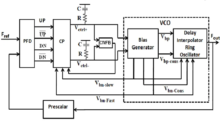
The modified block diagram of the self biased PLL adopting delay interpolation principle is shown in Figure.1. The functional blocks of the proposed PLL consists of Phase Frequency Detector (PFD), charge pump circuit (CP), Loop Filters (with capacitor C and resistor R), delay interpolator VCO and prescalar. In this proposed PLL except the VCO architecture all other functional blocks remains the same as described in [1]. The modified VCO functionality is based on the delay interpolator architecture [4]. The bias generator of the delay interpolator VCO is modified from the traditional self biased VCO to derive the required bias voltages from the differential control voltages to bias the delay elements as well as the charge pump circuits.
The traditional self biased VCO with single ended control voltage is modified to delay interpolator based VCO with differential control voltage, while the salient features required for static and dynamic supply rejection characteristics of the traditional self biased PLL are preserved.
[image:2.612.124.508.489.701.2]
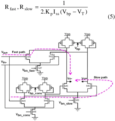
The architecture of the modified VCO is shown in Figure 2 that consists of a bias generator stage (Bias Gen) and a ring oscillator stage. The ring oscillator is designed with four delay elements. The bias generator stage provides the appropriate bias voltages Vbp, Vbp_cons, Vbn_cons,
Vbn_slow, Vbn_fast to the delay elements. The delay
element architecture is very similar to the one employed in [4] except that the resistive load is replaced by the symmetric load proposed in [1] and this enables the resistive load of delay interpolator VCO to operate as a linear resistor for the entire frequency range of operation and hence achieves dynamic supply noise rejection. The circuit schematic of the delay element consisting of a slow path and a fast path is shown in Figure 3. As in architecture [4], the buffer stage delay in the slow path is maintained constant, independent of the control voltage whereas the inverting stage delay in the slow path is controlled by Vbn_slow derived from
Vctrl- in the bias generator. The inverting stage delay
in the fast path is controlled by Vbn_fast generated
from Vctrl+ in the bias generator. In the symmetric
load, the current steered by Vbn_slow in the slow path
and the current steered by Vbn_fast in the fast path are
summed up. This summed up current Iss stays
constant and maintains a constant swing at the output node as in [4].
2.2 Design of modified VCO
The gain KVCO of the proposed VCO is
derived from the delay contributed by the individual delay element stages and is described as below.
The delay tp contributed by a single delay
[image:3.612.322.512.365.565.2]element is derived from its RC equivalent model given in Figure 4, and is expressed in Eq.(1-4).
Figure 2: Functional Block Diagram Of The Proposed Self Biased VCO
t
p= 0.69(K
fastτ
fast+ K
slowτ
slow). (1)
K
fast+ K
slow= 1 (2)
τ
fast=
R
fastC
L(3)
τ
slow=
(R
cons+ R
slow) C
L+ R
consC
cons(4)
In Eq.(1) τfast, τslow are respectively thetime constants determined by the fast and slow paths. The coefficients Kfast and Kslow defined in
Eq.(1) are the ratio of the current steered into slow path and fast path of the inverting stages with the total bias current Iss and satisfies the relation as
given in Eq.(2). In Eq.(3) the resistance Rfast is
derived from the inverting stage in the fast path and CL is the load capacitance at the output node of the
delay element stage. In Eq.(4) Rcons is the resistance
derived from the constant delay buffer stage in the slow path, Ccons is the load capacitance at the output
node of the constant delay buffer in the slow path.
Rslow is the resistance obtained from the inverting
stage in the slow path.
The resistance Rslow and Rfast are derived
from the symmetric load biased by Vbp. The
resistance thus obtained is expressed in Eq.(5).
) V (V I 2.K
1 R
, R
T bp ss p slow fast
− =
(5)
Figure 3: Functional Block Diagram Of The Proposed Self Biased VCO
[image:3.612.90.286.535.678.2]Here Kp represents K′(W/L), K′ denotes
process transconductance parameter and (W/L) denotes the aspect ratio of the transistors employed in the symmetric load.
The resistance Rcons is similarly derived
from the symmetric load that is biased by Vbp_cons.
The resistance thus obtained is expressed as
) T V cons bp (V cons I p 2.K
1 cons
R
− − =
(6) Here Icons and Vbp_cons are derived from a
constant bias voltage in the bias generator.
The VCO frequency is thus controlled by time the constants τfast and τslow and the coeffecients
kfast and Kslow. The time constants are independent
of control voltage, whereas the coefficients kfast and
Kslow play the role of transconductance of the
transistors steering current into the inverting stages of the slow and fast path.
Hence the KVCO characteristic is nonlinear
which is unlike the characteristic in traditional self biased VCO. But with the combination of delay interpolation principle and self bias principle, the VCO has the capability to exhibit wide operating frequency range very similar to the traditional self biased VCO.
2.3 Design of modified bias generator
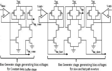
The bias generator is designed so that it preserves the supply rejection characteristic of the traditional self biased VCO. The circuit architecture of the modified bias generator modified from [1] is shown in figure.5. The bias voltage Vbp required for
biasing the symmetric load of slow and fast path inverting stage is generated in a half buffer replica stage, which is one half of the delay element stage similar to that adopted in [1]. The bias voltage Vbp
[image:4.612.94.287.561.684.2]generated in the replica buffer stage, is obtained by summing up the current steered by differential
Figure 5:Circuit Schematic Of Bias Generator
voltages Vbn_slow and Vbn_fast. Therefore the voltage
Vbp stays constant irrespective of the control
voltage since the bias voltages Vbn_slow and Vbn_fast
are differential. Since these bias voltages also bias the delay element stages, it ensures the lower limit of the constant swing in the delay element as Vbp
and hence meets the dynamic supply rejection characteristic of the traditional self biased PLL. The architecture also permits the bias voltage Vbp to
track supply voltage variations, with Vbn_slow and
hence retains the static supply rejection characteristics of traditional self biased VCO.
3. PROPOSED PLL SYSTEM DESIGN
Design of charge pump circuit and the PLL loop parameters are explained in the following subsections. The proposed PLL loop parameters are derived similar to the technique adopted in the traditional self biased PLL and is shown that it meets the requirements of constant damping factor and adaptive bandwidth over its entire operating frequency range as in [1].
3.1 Charge Pump circuit design considerations
The architecture of charge pump circuit is shown in Figure 6, and is very similar to the architecture employed in [1]. Similar to the design consideration applied in traditional self biased PLL, the charge pump device dimensions are chosen in certain relation with the device dimensions of the VCO delay elements. This helps in minimizing the mismatch between the currents steered by the UP and DN signals in the charge pump. Thus the device dimensions in VCO and hence the charge pump circuit device dimensions are chosen in such a way that the required operating frequency range is met and also the random noise generated from the charge pump circuit is as minimum as possible.
Figure 6:Architecture Of Charge Pump Circuit
Generating Differential Control Voltage
3.2 Proposed PLL loop parameter description
[image:4.612.322.525.565.670.2]generation circuit. The damping factor of a second order PLL is given in Eq.(7).
ζ
=
N .C .K I 2
R cp VCO
(7)
Charge pump current and loop filter resistance is derived from VCO’s delay element bias current, very similar to the traditional self biased PLL. The expression for ζ is similarly derived and is given in Eq.(8).
ζ
=
N . M . 2 C . K . 2 4 VCO x
y
(8)
The factor ‘x’ is defined by the ratio of the charge pump current Icp to the current defined in the
delay element Iss. The factor ‘y’ is used to define
resistance R of the loop filter similar to the technique employed in [1]. Here C is the capacitance of loop filter, N is the prescalar division factor and M is a constant defined as M= (0.69).2.n.
(9)
Here ‘n’ is the number of delay element stages incorporated in VCO.
By approximating VCO gain characteristic to be linear, from Eq.(9), it can be seen that ζ attains a constant value for the entire frequency range of operation very similar to the condition obtained in [1].
The proposed PLL loop bandwidth is made to track the operating frequency similar to [1]. The resonant frequency ωn for a second order
PLL is expressed as given in Eq.(10).
ω
n=
C . N K . I .ss VCOx
(10)
The ratio of reference frequency ωref to ωn
for the proposed self biased PLL is derived similar to that in [1], using the conditions given in Eq.(11).
R
cons= z.R
fast= z.R
slow.. (11)In Eq.(11) z is a constant. Using this condition, the derived ωref to ωn is expressed as in
Eq.(12). + + + π = ω ω L cons slow fast L VCO p C C . 1 K K 1 C C K . k 2 M 2 z z x n ref
(12) The ratio ωref to ωn is thus found to be
constant dependent on ratio of capacitances approximating KVCO to be a constant. Thus the
system possesses adaptive bandwidth nature, independent of process variations similar to that in [1].
4. PROPOSED PLL DESIGN SPECIFICATIONS AND SIMULATION RESULTS
A traditional self biased PLL was designed to compare the jitter performance with the proposed PLL. The traditional self biased PLL was first designed with loop parameters ζ to set to be 1, and the ratio ωref to ωn was set to be 15. Also, the
traditional self biased VCO was designed with a tuning range of 800MHz to 2.7GHz. For the proposed differential self biased PLL, the VCO was designed with a similar tuning range. The charge pump bias currents, loop filter R and C values, and the prescalar value (N=16) was set to be identical for both cases. With these system parameters chosen, the proposed differential self biased PLL and the traditional self biased PLL will have identical loop parameters ζas 1andωref to ωn as 15
and hence their performance comparison is expected to be fair.
4.1 Simulation Results
Simulation results are presented for the proposed as well as the traditional self biased PLL. Circuit simulations were carried out using 0.18µm CMOS process in Cadence.
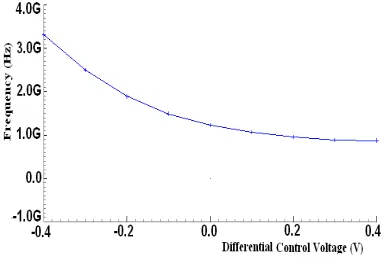
[image:5.612.321.513.490.621.2]The proposed VCO’s gain characteristic is shown in Figure 7. Even though the gain characteristic is observed to be nonlinear, due to the combination of delay interpolation and self bias principle, the proposed VCO exhibits a wide operating range of frequencies 850MHz to 2.7GHz.
Figure 8a: Traditional Self Biased VCO Swing
Figure 8b:Proposed Self Biased VCO Swing
Constant swing obtained from the proposed VCO is shown in comparison with the output swing obtained from the traditional VCO in Figure 8a,b. It can be seen from Figure8a. that the traditional VCO swing varies with operating frequency. At 900MHz, the VCO swing as seen from the waveform labeled (1), is observed to be 0.8V and at 2.8GHz as seen from the waveform labeled (2), it is observed to be 1.1V. The constant VCO swing retained by the proposed delay interpolator VCO is shown in Figure8b. A constant VCO swing of 1.1V is observed at the extreme frequency of 900MHz marked as (3) and at the other extreme frequency of 2.8GHz marked as (4).Thus the proposed VCO is observed to retain its swing to 1.1V over its entire operating frequencies.
The bias voltage transients of the traditional and proposed self biased PLL are shown in Figure 9 at an operating frequency of 2.1GHz. From the bias voltage transients Vbn of the
traditional self biased PLL and Vbn_slow and Vbn_fast
of the proposed PLL, it can be observed that both the system settle times are very closer. The traditional self biased PLL is observed to settle at
110ns (14 reference clock cycles) and the settling time of the proposed self biased PLL is found to be very closer at 114ns (15reference clock cycles) with a frequency step of 700MHz from the free running frequency.
Figure 9:Capture Transients Of Bias Voltages Of The
Traditional And The Proposed Self Biased PLL At 2.1ghz
Figure 10: Jitter Performance At 2.1ghz Output Frequency
The peak to peak jitter measure using an eye diagram plot is shown in Figure 10 for the two architectures at the operating frequencies of 2.1GHz. The peak to peak jitter measure for the traditional self biased PLL architecture is 12.4ps (0.026UI) where as for the proposed self biased PLL it is observed to be 5.9ps (0.012UI), thereby the proposed PLL shows 52% improvement in jitter performance.
[image:6.612.318.513.349.437.2](0.013UI) showing 64% improvement. There is a marginal degradation while comparing jitter performance improvement with the noiseless case of 1GHz output frequency, as the bias generator of the proposed PLL drives a larger capacitive load, hence the gain at 100MHz supply noise of the proposed PLL bias generator degrades when comparedwith the gain of thetraditional self biased PLL bias generator.
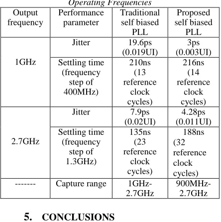
Table 1 : Performance Comparison At Extreme Operating Frequencies
Output frequency
Performance parameter
Traditional self biased
PLL
Proposed self biased
PLL
1GHz
Jitter 19.6ps
(0.019UI)
3ps (0.003UI) Settling time
(frequency step of 400MHz)
210ns (13 reference
clock cycles)
216ns (14 reference
clock cycles)
2.7GHz
Jitter 7.9ps
(0.02UI)
4.28ps (0.011UI) Settling time
(frequency step of 1.3GHz)
135ns (23 reference
clock cycles)
188ns (32 reference clock cycles) --- Capture range
1GHz-2.7GHz
900MHz-2.7GHz
5.
CONCLUSIONSIt is demonstrated in this paper that it possible to suitably combine the traditional self biased PLL and the delay interpolator VCO in order to derive the benefits of both the schemes. The proposed PLL shows significant improvement in jitter while compared with the traditional self biased PLL without exhibiting any degradation in the settling time. Since the system bandwidth is adaptive, the proposed PLL captures over a wide frequency span of 1.7GHz. It was also observed that the proposed scheme is capable of jitter improvements ranging from 46% to 85 % with marginal degradation in the capture time and supply rejection. It was also shown that the VCO swing in the proposed PLL has a constant signal swing 1.1V over the entire operating frequency range. Further increase VCO swing might be possible and this will be taken up for future work.
REFRENCES:
[1] John G. Maneatis, “ Low-Jitter Process-Independent DLL and PLL Based on Self-Biased Techniques,” IEEE Journal Of Solid State Circuits, Vol. 31, No.11, pp1723-1732, November 1996.
[2] Nasser Kurd, Praveen Mosalikanti, Mark Neidengard, Jonathan Douglas, and Rajesh Kumar, ”Next Generation Intel® Core™ Micro-Architecture (Nehalem) Clocking”, IEEE Journal Of Solid State Circuits, Vol. 44, No. 4, pp1121-1129, April 2009.
[3] Blaine Stackhouse, Sal Bhimji, Chris Bostak, Dave Bradley, Brian Cherkauer, Jayen Desai, Erin Francom, Mike Gowan, Paul Gronowski, Dan Krueger, Charles Morganti, and Steve Troyer, “A 65 nm 2-Billion Transistor Quad-Core Itanium Processor”, IEEE Journal Of Solid State Circuits, Vol. 44, No.1, pp 18-31, January 2009.
[4] Seema Butala Anand, Behzad Razavi, “A CMOS Clock Recovery Circuit for 2.5-Gb/s NRZ Data”, IEEE Journal of Solid-State Circuits, Vol.36, No.3, pp.432-439, March 2001.
[5] D.Duarte, S. Hsu, K. Wong, M. Huang and G. Taylor, “Interpolated VCO design for low bandwidth, low jitter, self biased PLL in 45 nm CMOS,” IEEE Custom Integrated Circuits Conf. 2010.
[6] J Song Ying, Wang Yuan, Jia Song, Zhao Baoying, “A novel calibration technique applying to an adaptive-bandwidth PLL,” International Conf. on Solid State and Integrated Circuit Technology, pp1933-1936, Oct. 2008.