5
VIII
August 2017
Analysis of Low Voltage Bulk-Driven High Swing
Cascode Current Mirrors for Low Voltage
Applications
P. Devendra Kumar1, D.Vijay Kumar2
1(M.Tech in VLSI &EMBEDED SYSTEM DESIGN, Student), 2Assistant Professor, Electronics and Communication Engineering
Department
Velagapudi Ramakrishna Siddhartha Engineering College, Jawaharlal Nehru Technological University -Kakinada, Kanuru, Vijayawada, Andhra Pradesh
Abstract: Now a days Low voltage along with low power topologies of analog and mixed signal designs have gained enormous importance due to increased demand of portable devices. The bulk-driven technology is emerging as an important design technique to achieve intensifies performance in low voltage analog circuits. Low voltage self-biased high swing cascode current mirror employing bulk-driven nmos transistor is proposed and proposed circuit has to be simulated in cadence tool, and different current mirrors like wilson current mirror and triple cascode current mirror are implemented under bulk-driven technology and simulated in cadence tool, and the results are compared with the gate-driven technology .
Keywords: Bulk-Driven, High swing, cascode, current mirror, low voltage
I. INTRODUCTION
From the last few decades the market for portable electronic systems such as a wireless Communication devices, and consumer electronics, etc. is continuously expanding day by day, So there is a improvement need for the development of low-voltage (LV) and low-power (LP) circuit techniques and system building blocks. Not only low-voltage but also low-power operation are of tremendous importance for advisable applications. The Low-voltage operation is demanded because it is desirable to use as less batteries as possible for size and weight considerations, It is necessary to ensure a reasonable battery lifetime so we use low power consumption technique. An important factor regarding analog circuits is that; the threshold voltages of future standard CMOS technologies are not expected to decrease much below what is availableon nowadays. The MOS transistor is a four terminal device; it is mostly used as a three terminal device because the bulk terminal is connected to the source terminal or to the drain terminal, to Vdd or to Vss. So, a large number of possible MOS circuits are overlooked; hence a good solution to overcome the threshold voltage is usage of the Bulk-driven technology. The principle of the Bulk-driven technology is that; the gate-source voltage is set to sufficientvalue to create an inversion layer for the MOSFET.
By applying an input signal to the bulk terminal of the MOSFET. By this way, the threshold voltage can be either reduced or removed from the signal path. The operation of the Bulk-driven MOS transistor is like a JFET i.e. a depletion type device, it can work under zero, negative, or even slightly positive biased conditions.That means the threshold voltage requirements are removed from signal path.
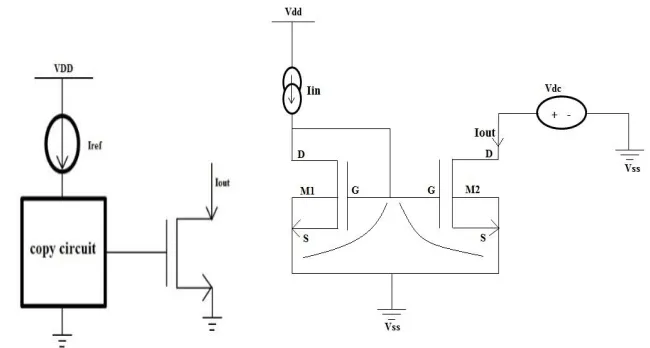
Fig. 1 current mirror circuit Fig. 2 Basic current mirror circuit
II. BASIC CURRENT MIRROR
Current mirror is a two port device,it is designed to generate a scaled replica of an input current at a high-impedance output node terminal. It keeps the output current constant regardless of loading. The major factors influencing the performance of a good current mirror are, its operating range,and bandwidth, output resistance and the mini mum voltage drop required across input and output terminals of the current mirrorcircuite. This voltage drop is required to keep the transistors of the current mirror in saturation mode. in the above fig the source is connected to the ground so the two transisters M1 and M2 gate source voltages are same, because of diode connection the transistor M1 is in saturation region and to make the M2 in saturation region we have to take VGS > VTH and VDS > VGS-VTH. If both transisters are in saturation region the the same inutcurrent is assing trough the drain terminal of the M2transister.Current equation in saturation region is:
ID=µncox ( ) (Vgs-Vth )2...( 1 )
With channel length modulation effect: ID=µncox ( ) (Vgs-Vth )2(1+λVds)…………..( 2 )
III. CASCODE CURRENT MIRROR
A cascode current mirror circuit is capable of producing an output current that is a direct function of an input current received by that device. The cascoded current mirror includes at least two portions connected together in a cascodemanner.This feedback connection can, for example, be a buffering connection. Voltage signals are generated by this device that can be used to drive and control additional output stages. Each such additional output stage is capable of producing an additional output current. Regulated cascode technique greatly increases the D.C. gain of cascode amplifier without sacrificing speed or output swing. Regulated Cascode current mirror produces more constant results than other cascode current mirror structures, here the negative feedback concept is used. The cascode can improve the output impedence of the circuit.
[image:3.612.117.300.594.706.2]
Self biasedcascode current mirror is used to achieve better matching current carecteristics at input and output nodes of the circuit.and it is also used to achive high output impedence. In this circuit the output resistence of the circuit is increased by a factor ofgmr0where gmis the transconductence and r0is the output resistence of the circuit.
IV. BULK-DRIVEN CURRENT MIRROR
A. Simple Bulk-Driven Current Mirror
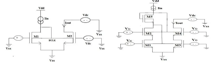
Bulk-driven techniques are applied to the mosfetonly that can be fabricated in its own separate well.The operation of the bulk-driven mosfet is much like a jfet. The conceptual schematic of the gate bulk-driven current mirror shown in fig 4(a). It consists of Q1,Q2cmostransisters and input current (Iin) and Iin flows through Q1 transister. Iout try to follow the Input current or reference current (Iref) .Here the input signal is applied the bulk terminal instead of the gate terminal to lower the threshold voltage requirement. And at the gate terminal sufficient VG applied to operate the mosfet in saturation region.
Fig 4(a) simple bulk-driven current mirror Fig 4(b) self-biased bulk-driven cascode current mirror
B. Bulk-Driven Self-Biased Cascode Current Mirror
The proposed bulk-driven self-biased cascode current mirror shown in figure4(b). In this circuit a constent voltage VDC>VTH is applied at the gate terminal of the each mosfet, which enables the to be formed. And here the input signal is applied at the bulk terminal instead of the gate terminal so it forms an bulk-drain connection instead of the gate-drain connection. Since the requirement of the threshold voltage is removed from the signal path of the circuit.and voltage drop is lowered at the input and output terminals of the device, hence it makes the proposed circuit operate at lower supply voltages.In this circuit the gate voltage is fixed ir ensures the dependency of the mosfet current on bulk-drain voltage, based on the below equation 3(a).
ID(sat)= ( VGS-VTo-ϒ − +ϒ )2 ………..3( a)
AndV
ds>Vgs-Vt
Where β=µncox , and w/l is the aspect ratio of the transistor and is the absolute fermi potensial , VTo is the zero bias threshold voltage and ϒ is the body effect coefficient.The current across the mosfet can be determined by the equation (3) for variation in potensialVbs and here the values of Vbs is less than the threshold voltages to ensure negligible bulk current in the circuit. The current mirror operation in the proposed circuit is implemented by constent bulk source potensial M1 and M3 and same being copied at M2 and M4 transisters.
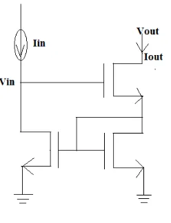
[image:4.612.90.523.275.403.2]V. WILSON CURRENT MIRROR
The Wilson current mirror that function well at all current levels from low range week inversion region to strong inversion region. And these current mirrors can be operate at the low level power supply voltages and results a high output voltage swing with cascode type incremental of the output impedence.
Fig 5(a) wilsen current mirror
A. Simple Wilsen Current Mirror
The Wilson current mirror gains a high incremental output resistance. Any increase in the output current due to an increase in the output voltage through output transistor’s Early effect that is sensed by the simple current mirror circuit whose input is in series with the output of the transistor. This simple mirror feeds back the output current to the input node of the circuit ,and reducing the gate voltage of the ouput transistor, thereby reducing its channel current and compensating the original current increase.
does not normally need to move by very much to compensate such variations of output current , if the output transistor enters its saturation region, the incremental output conductance increases to the point that it is comparable to the transistor’s incremental transconductance gain. In this case, the input voltage will change by more than the output voltage in an attempt to compensate for changes in the mirror’s output current. We shall take the output voltage at which the output transistor’s incremental output conductance is on a par with it’stransconductance to be the Wilson mirror’s output compliance voltage. If the output voltage drops below this level, the output current decreses precipitously to zero while the input voltage rises rapidly towards the positive power supply.
[image:5.612.242.366.147.309.2] [image:5.612.140.505.517.697.2]B. Bulk-Driven Wilsen Current Mirror
The bulk driven wilsen current mirror shown in fig 5(c).here the input signal is applied at the bulk terminal instead of the gate terminal to reduce the threshold voltage requirement.
Here M1 and M2 and M3, M4 are the four mostransisters, In the above diagram the input signal is Iin and it is connected to the bulk terminal of the mosfet M2 and M4. The fixed gate voltage VG is connected to the gate of each transistor for channel formation .Here we have apply the drain source voltage of the transistor M4 to make the transistor in the saturation region. Current equation in saturation region of the bulk driven transiter is given as
ID(sat)= ( VGS-VTo-ϒ 2 f−Vbs +ϒ 2 )2 ( 4 )
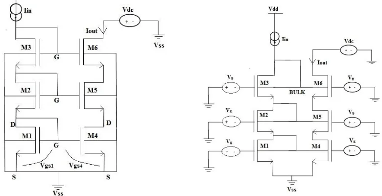
VI. TRIPLE CASCODE CURRENT MIRROR
A. Triple Cascode Gate- Driven Current Mirror
The output impedence can be further improved by adding one more cstaage to the double cascode configuration, the increase of cascode connection increases the total output impedence of the cirtuit and the gain also increases. In the fig 6(a) Shown below the reference current is connected to the drain of the mosfet M3 and the M1 is another transistor which is cascaded to the transisters M2 and M4 and M4 is cascaded to the transistor M5 and M6.
Here the source of the transisters M1 and M4 are connected to the ground so their gate-source voltages are same and Vdc for the mosfet M6 is chosen such as to make the transisters in saturation region. The transistor M3 is diode connected so it is in saturation region .bymakingall transistor in saturation region the same reference current is passing through the output terminal.
Fig. 6(a) triple cascode current mirror Fig. 6(b) Bulk-driven triple cascode current mirror
B. Triple Cascode Bulk- Driven Current Mirror
The fig 6(b) shown below is the triple cascode current mirror with bulk-driven technology. Here the input signal is applied at the bulk terminal of the transistor instead of the gate terminal to reduce the tresold voltage requirement hence the circuite can be simulated under minimum input voltages and the cascading connection also increases the output impedence of the circuit and the outut swing also increases hence the band width also increases.
[image:6.612.115.505.369.569.2]VII. PROJECT OUTPUT WAVE FORMS
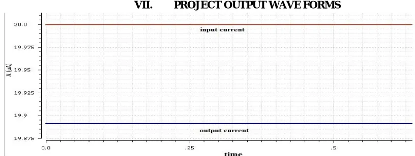
[image:7.612.71.528.283.693.2]Fig 7.1 input vs output current variations of simple current mirror
Fig. 7.2 minimum input voltage required for the cascode current mirror
Fig. 7.3 Iin VS Iout of the self-biased bulkdriven cascode current mirror
[image:7.612.73.531.286.418.2]Fig. 7.5 Perametric analasis of proposed current mirror Iout VS different length of transister
Fig .7.6 Perametricanalasis of proosedcktIout VS differength width with same length
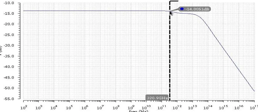
[image:8.612.94.525.496.696.2]Fig. 7.8 minimum input voltage required for bulk -driven wilsen current mirror
Fig 7.9 Iin VS Iout of the bulk-driven triple cascode current mirror
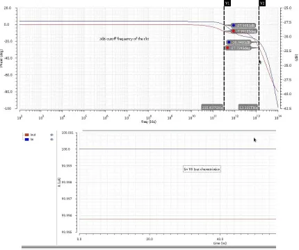
[image:9.612.92.522.311.671.2]Fig. 7.11 maximum cut off frequency of the triple cascode current mirror
Fig 7.12 magnitude and phase response of the bulk-driken Wilson current mirror
VIII. CONCLUSION
IX. COMPARISION TABLE OF ALL CURRENT MIRROR RESULTS
Current Mirror (C.M) Type Min. i/p Voltage (V) o/p Voltage (V) o/p Resistance
(K Ω)
Simulation Technology Used (nm)
No. of. Transistors
Upper cut-off frequency (Hz)
Simple C.M 0.6 0.6 140 180 2 5 MHz
Cascode C.M 1.37 1.39 267 180 4 7 MHz
Self-biased Cascode C.M
0.77 0.65 139 180 5 7 MHz
Bulk-driven C.M 0.5 0.67 164 180 2 6 MHz
Bulk-driven self-biased cascode C.M
0.3 0.38 135 180 5 10 MHz
Wilson C.M
0.8 0.9 225 180 4 5 GHz
Bulk-driven Wilson C.M
0.47 0.85 203 180 4 7 GHz
Triple cascode C.M
2.45 2.3 255 180 6 6 GHz
Bulk-driven triple cascade C.M
1 1.1 243 180 6 30 GHz
REFERENCES
[1] B.J. Blalock, P.E. Allen, G.A. Rincon-Mora, Designing 1-V op amps using standard digital CMOS technology, IEEE Trans. Circuits Syst.Analog Digital Signal Process. 45 (1998) 769–78
[2] [2] J. Rosenfeld, M. Kozak, E.G. Friedman, A bulk-driven CMOS OTA with 68 dB DC gain, IEEE International Conference on Electronics, Circuits and Systems. (ICECS 2004) 5–8
[3] J. Rosenfeld, M. Kozak, E.G. Friedman, A 0.8 V high performance OTA using bulk-driven MOSFETs for low power mixed-signal SOCs, IEEE International Conference on SOC. (2003) 245–246.
[4] R. He, L. Zhang, Evaluation of modern MOSFET models for bulk-driven applications, 51st Midwest Symposium on Circuits and Systems. (MWSCAS (2008) 105–108.
[5] Christian Je´sus B. Fayomi, M. Sawan, G. Roberts, Reliable circuit techniques for low-voltage analog design in deep submicron standard CMOS: a tutorial, Analog Integr. Circuits Signal Process. 39 (2004) 21–38
[6] J.M. Carrillo, R. Perez-Aloe, J.M. Valverde, J.F. Duque-Carrillo, G. Torelli, Compact low-voltage rail-to-rail bulk-driven CMOS opamp for scaled tech- nologies, European Conference on Circuit Theory and Design. (ECCTD 2009) 263–266.
[7] J.M. Carrillo, G. Torelli, R. Perez-Aloe, J.F. Duque-Carrillo, 1-V rail-to-rail CMOS OpAmp with improved bulk-driven input stage, IEEE J. Solid-State Circuits 42 (2007) 508–517
[8] Y. Haga, H. Zare-Hoseini, L. Berkovi, I. Kale, Design of a 0.8 V fully differential CMOS OTA using the bulk-driven technique, IEEE Int. Symp. Circuits Syst. 1 (2005) 220–223.\