SC14425
Complete Baseband processor for DECT Base Stations
with Caller-id and Handsfree
General Description
The SC14425SC14425 is a 3.3 Volt CMOS IC optimized to handle all the audio, signal and data processing needed within a DECT base station. An ADPCM transcoder, a very low power 14 bit Codec and Analog Frontend are in-tegrated. Direct connections towards analog or ISDN line interface.
The SC14425 has an on-chip dedicated flexible DSP op-timized for telecom applications caller-id, handsfree and allows easy connection to digital telephone answering machine devices.
The SC14425 is designed to be compatible with many radio interfaces. A dedicated TDMA controller handles all physical layer slot formats and radio control. The integrat-ed National Semiconductor’s standard CR16B processor core takes care of all the higher protocol stack. Program-mable I/O ports can be configured as chip selects for I/O expanders, Serial Flashes, interrupt source or I/O. A dig-ital serial interface can be configured to interface to
indus-try-standard c odecs and ISDN devices with µ-Law, a-Law,
linear or transparent data formats.
Features
nIntegrated DECT base band transceiver optimized for
GAP base stations according to ETS 300 175-2,3 & 8.
n2.7 to 3.3 Volt operating voltage.
nEmbedded 16 bit CompactRISCT M CR16B
Microproc-essor with In System Emulation (ISE) mode.
nOn-chip 6kByte Data Memory.
nEmbedded flexible dedicated DSP executing Caller-id
(CID), Caller-id on Call Waiting (CIDCW) and hands-free, two echo cancellers, two echo suppressors, ex-tended DTMF detection, DTMF generation, sidetone and artificial echo loss.
nTwo full duplex 32 kbits/sec ADPCM transcoder.
nOn-chip Dedicated Instruction Processor (DiP) for all
TDMA based events, which supports 1.152MHz, 0.576MHz and 0.288MHz data rates.
nProtected and unprotected full and double slot B-fields
nStandard DECT encryption with different keys for
different MAC-connections.
nAt least 6 MAC connections can be handled
simultane-ously.
nFlexible three wire interface to radio front synthesizer.
nOne 14-bit linear CODEC with programmable gain
nPeak hold ADC for RSSI measurement
nTwo input 8 bit successive approximation ADC.
nThree general purpose I/O ports with programmable
in-terrupts
nFull duplex UART, SPIT M and MICROWIRET M interface.
nFlexible 8 kHz synchronous Serial interface to external
codecs and ISDN interface circuits.
nTwo general purpose timers and watch dog timer.
nProgrammable chip selects to 8 bit wide ROM, SRAM
NAND Flash Memory and I/O expanders.
nTwo Capture timers for frequency measurement for
e.g. metering, ringing and call progress tone detection.
n100 pin TQFP-100 package.
Note 1: CompactRISCTM is a trademark of National Semiconductor
Cor-poration, SPIT M is a trademark of Motorola.
________________________________________________________________________________________________
System Diagram
ISDN or ISDNPRELIMINARY
FEBRUARY 20001
4
4
2
5
C
o
m
p
le
te
B
a
s
e
b
a
n
d
p
ro
c
e
s
s
o
r
fo
r
D
E
C
T
B
a
s
e
S
ta
tio
n
s
Copyright 2000 National Semiconductor Corp. 2 www.national.com
S
C
1
4
4
2
5
C
o
m
p
le
te
B
a
s
e
b
a
n
d
p
ro
c
e
s
s
o
r
fo
r
D
E
C
T
B
a
s
e
S
ta
tio
n
s
1.0 CONNECTION DIAGRAM
Order Number SC14425XVJG (Standard version) X=silicon revision
See NS Package Number VJG100A
Note 1: All digital outputs can sink/source 2 mA unless otherwise specified. All digital inputs are Schmitt trigger types. After reset all I/Os are set to input
and all pull-up or pull-down resistors are enabled unless otherwise specified. PU = Pull-up resistor enabled, PD = Pull-down resistor enabled, I = input A-I, B-I = In Boot mode A or B input and pull-up or pull-down resistor disabled,
A-PD, B-PU = In Boot mode A, Pull-down resistor enabled. In Boot mode B, pull-up resistor enabled.
Note 2: Reset state of address and WRn, RDn pins:
Hi-Z/1 means Hi-Z if RSTn is LOW, if RSTn goes HIGH is takes 32 SCLK cycles = 25 usec before these pin drives a ‘1’.
Note 3: 5 Volt protection pads: type *P may NOT be connected to an external pull down resistor
DAB0 AD0 AD1 AD2 AD3 P1[6] HOLDn RSTn Xtal1 DAC AVS2 AVD2 LRS2+ LRS2- VREF2- MIC2-AGND MIC2+ VREF2+ CAP2+ CAP2-N.C. CAP SCLK VDD VSS PD7 PD6 PD5 PD4 PD3 PD2 PD1 DAC2 MEN1n SO SK VDDRF RDI CMPREF RSSI AVD AVS TDO RFCLK P 0 [3 ] P 0 [4 ] P 0 [5 ] P 0 [6 ] P 0 [7 ] P 1 [0 ] P 1 [1 ] P 1 [2 ] P 1 [3 ] P 1 [4 ] P 2 [0 ] A D C 2 V D D V S S T P P 2 [3 ] P 2 [4 ] P 2 [5 ] 1 2 3 4 5 6 7 8 9 10 11 12 13 14 15 16 17 18 19 20 21 22 23 24 25 75 74 73 72 71 70 69 68 67 66 65 64 63 62 61 60 59 58 57 56 55 54 53 52 51 1 0 0 9 9 9 8 9 7 9 6 9 5 9 4 9 3 9 2 9 1 9 0 8 9 8 8 8 7 8 6 8 5 8 4 8 3 8 2 8 1 8 0 7 9 7 8 7 7 7 6 2 6 27 28 29 30 31 32 33 34 35 36 37 83 39 40 41 42 43 44 45 46 47 48 49 50 SC14425 P 1 [5 ] A D 4 A D 5 A D 7 A D 1 2 A D 1 5 A D 1 6 W R n A D 1 7 A D 1 4 A D 8 A D 9 A D 1 1 R D n A D 1 0 R C S n V S S V D D D A B 7 D A B 6 D A B 5 D A B 4 D A B 3 A D 1 3 A D 6 C S 1 T O N E A D 1 9 C L K 1 0 0 IN T n 1 IN T n 0 IN T n 2 IN T n 3 IN T n 4 P W M S T R 1 S T R 0 IC L K C O U T C IN P 2 [1 ] P 2 [2 ] S C K P 1 0 _ IN T S E N S D I S D O A D C 1 P 2 [7 ] P 2 [6 ] A D C 0 MI INTn7 ACSn INTn6 D A C 0 P1[7] H O L D A C K N R E A D Y N.C. N.C. N.C. P 0 [0 ] P 0 [1 ] P 0 [2 ] U T X U R X C S 0 DAB 1 DAB2 C S 2 A D 1 8 IN T 5 n
F e b ru a ry 2 0 0 0 , 3 BMC CR16B SBI P0 P1 P2 ICU UART PWM Dedicated Seq RAM Shared 8 bit DAC 8 bit ADC Xtal Boot ROM Bus arbiter Clock/Data Recovery 6 bit DAC Gaussian Filter Instruction Processor peakhold ADC Watchdog Timer0 Timer1 TONE AD(19..0) DAB(7..0) P 2 .7 P 1 .7 P 1 .0 A C S N R C S N W R N R D N MI A V S X T A L 1 C A P Osc CLOCK RFCLK TDO RDI RSSI CMPREF V D D 1 ,2 ,3 V S S 1 ,2 ,3 R S T N 0 S C L K H O L D N C S 0 ,1 ,2 ADC1 P 2 .0 .. P 0 .7 P 0 .0 Data RAM Data RAM Timer/ Counter DAC Debounce Timer VDDRF Capture ADC2 P1.0 SPI C L K 1 0 0 ECZ1,2 1,2 P W M 8 bit DAC DAC2 ADC0 DAC0 H O L D A C K R E A D Y
Copyright 2000 National Semiconductor Corp. 4 www.national.com
S
C
1
4
4
2
5
C
o
m
p
le
te
B
a
s
e
b
a
n
d
p
ro
c
e
s
s
o
r
fo
r
D
E
C
T
B
a
s
e
S
ta
tio
n
s
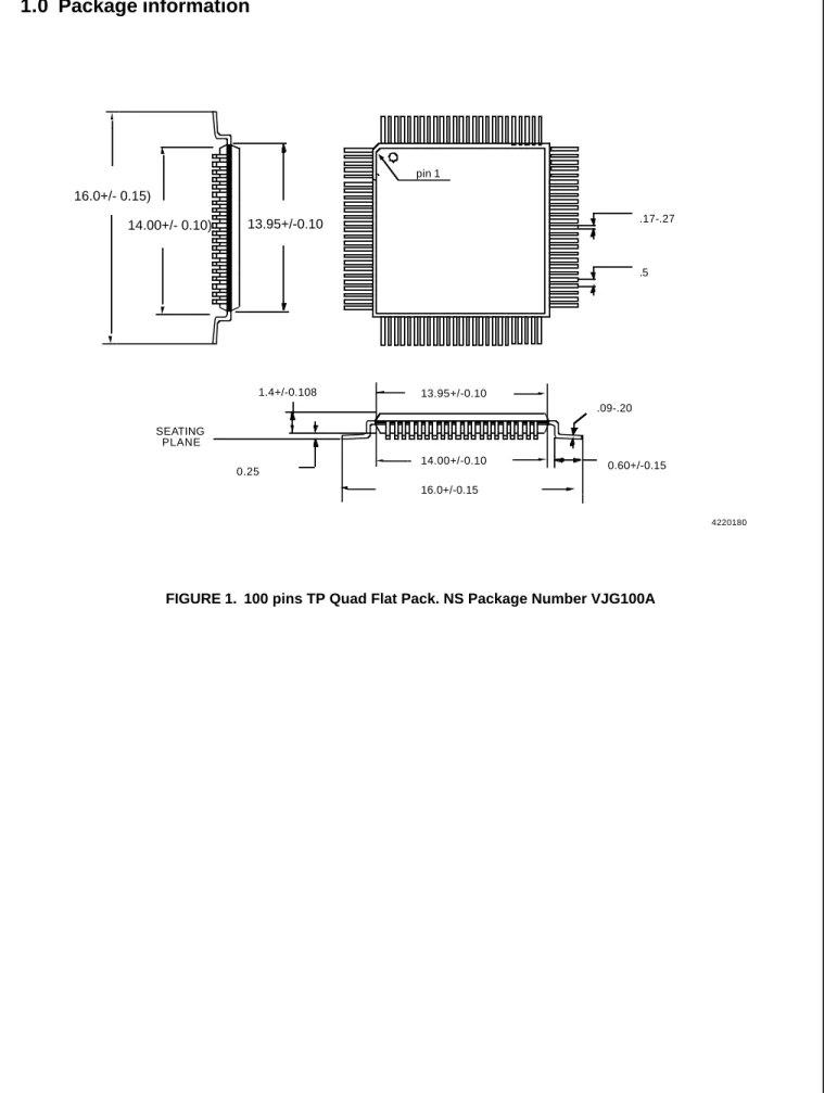
1.0 Package information
FIGURE 1. 100 pins TP Quad Flat Pack. NS Package Number VJG100A
.17-.27 .5 .09-.20 0.60+/-0.15 1.4+/-0.108 0.25 14.00+/- 0.10) 16.0+/- 0.15) 13.95+/-0.10 13.95+/-0.10 14.00+/-0.10 16.0+/-0.15 SEATING PLANE 4220180 pin 1
1
4
4
2
5
C
o
m
p
le
te
B
a
s
e
b
a
n
d
p
ro
c
e
s
s
o
r
fo
r
D
E
C
T
B
a
s
e
S
ta
tio
n
s
2.0 Product status definitions
National Semiconductor B.V reserves the right to make changes without notice to any products herein to improve reliability, function or design. National does not assume any liability arising out of the application or use of any product or circuit de-scribed herein; neither does it convey any license under its patent rights, nor the right of others.
________________________________________________________________________________________________
.
Definition of Terms
Data Sheet
Identification Product Status Definition
Advance Information Formative or In Design
This data sheet contains the design specifications for product development. Specifications may change in any manner without notice.
Preliminary First Production
This data sheet contains preliminary data. Supplementary data will be published at a later date. National Semiconductor Corporation reserves the right to make changes at any time without notice in order to improve design and supply the best possible product.
No Identification Noted Full Production
This data sheet contains final specifications. National Semiconduc-tor Corporation reserves the right to make changes at any time without notice in order to improve design and supply the best possi-ble product.
Obsolete Not In Production
This data sheet contains specifications on a product that has been discontinued by National Semiconductor Corporation. The datash-eet is printed for reference information only.
LIFE SUPPORT POLICY
NATIONAL’S PRODUCTS ARE NOT AUTHORIZED FOR USE AS CRITICAL COMPONENTS IN LIFE SUPPORT DEVICES OR SYSTEMS WITHOUT THE EXPRESS WRITTEN APPROVAL OF THE PRESIDENT OF NATIONAL SEMICONDUCTOR CORPORATION. As used herein:
1. Life support devices or systems are devices or systems which, (a) are intended for surgical implant into the body, or (b) support or sustain life, and whose failure to per-form, when properly used in accordance with instructions for use provided in the labeling, can be reasonably ex-pected to result in a significant injury to the user.
2. A critical component is any component of a life support device or system whose failure to perform can be rea-sonably expected to cause the failure of the life support device or system, or to affect its safety or effectiveness.