140
Optimization Of Power For Sequential Elements In
Pulse Triggered Flip-Flop Using Low Power
Topologies
Saranya. L, Prof. S. Arumugam
ABSTRACT : - The choice of flip-flop technologies is an essential importance in design of VLSI integrated circuits for high speed and high performance CMOS circuits. The main objective of this project is to design a Low-Power Pulse-Triggered flip-flop. Flip-flops are the major storage elements in all SOC’s of digital design. They accommodate most of the power that has been applied to the chip. Flip-flop is one of the most power consumption components. It is important to reduce the power dissipation in both clock distribution networks and flip-flops. The power delay is mainly due to the clock delays. The delay of the flip-flops should be minimized for efficient implementation. Here three kind of conventional pulse-triggered flip-flop are designed. First, the implicit Pulsed Data-Close to output (ip-DCO) pulse-triggered flip-flop. Second, the Modified Version of Hybrid latch flip-flop (MHLFF) and third is the Single-ended Conditional Capturing Energy Recovery (SCCER) flip-flop. These three flip-flops are studied and designed. The comparison of low power pulse triggered flip-flops between SAL ,SVL logics is carried out and the best power -delay-performance is obtained. The simulation results are obtained with Tanner simulation tool.
Keywords :- Flip-flop,ip-DCO,MHLFF,SCCER .
————————————————————
1. INTRODUCTION
Flip-Flops and latches are the basic elements for storing information. One latch or Flip-Flop can store one bit of information. The main difference between latches and flip-flops is that for latches, their outputs areconstantly affected by their inputs as long as the enable signal is asserted. In other words, when they are enabled, their content changes immediately when their input change. Flip-flops, on the other hand, have their content change only either at the rising or falling edge of the enable signal. This enable signal is usually the controlling clock signal. After the rising or falling edge of the clock, the flip-flop content remains constant even. There are basically four main types of latches and flip-flops: SR, D, JK, and T. The major differences in these flip-flop [13] types are the number of inputs they have and how they change state. For each type, there are also different variations that enhance their operations. Figure 1(a), (b) illustrates the difference between positive edge triggered flip flop and an active high latch. As it can be seen in this figure, possible changes of input can be seen at the output of the latch while it is transparent
Fig 1 (a) Active High latch (b) Positive Edge Triggered Flip-Flop
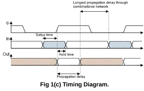
The performance of a flip-flop is measured by three important timings and delays: propagation delay (Clock-to-Output), setup time and hold time. They reflect in the system level performance of the Flip-Flops [5]. Setup time and hold time define the relationship between the clock and input data as shown in the Figure 1(c).Setup time and hold time describe the timing requirements on the D input of a Flip-Flop with respect to the Clk input. Setup and hold time define a window of time which the D input must be valid and stable in order to assure valid data on the Q output. Setup Time (Tsu) Setup time is the time that the D input must be valid before the Flip-Flop samples. Hold Time (Th) – Hold time is the time that D
input must be maintained valid after the Flip-Flop samples. Propagation Delay (Tpd) – Propagation delay is the time that takes to the sampled D input to propagate to the Q output.
Fig 1(c) Timing Diagram.
2. EXISTING FLIP-FLOP DESIGN
2.1. IMPLICIT PULSED DATA CLOSE TO OUTPUT Ip-DCO is one of the implicit kinds of flip-flop where the pulse is generated inside the flip-flop itself. Here the input node is kept closer to the output node so that it has less data to output delay, hence the name DCO. Here the clock signal and complement of the clock signal generates a narrow pulse of short duration. During this pulse width the data to output transition occurs.
______________________________
Saranya. L, PG Scholar, SNS College of Tech, Coimbatore, [email protected]
141
2.1.1. OPERATION OF ip-DCO
The implicit type flop generates the pulse inside the flip-flop. The circuit diagram of ip-DCO is shown in the figure 2. In ip-DCO the clock signal and complement of the clock signal generates a narrow pulse of short pulse width .During this pulse the output follows the input.
Figure2. Circuit diagram for ip-dco
In this circuit the inverters I1, I2, I3 are the delay circuit used for generating the pulse. The inverters I5 and I6 are used to latch the data. X is the internal node in this circuit. Only during the rising edge of the clock pulse, a flip-flop generates the narrow pulse and pulse width of pulse is according to delays specified in the inverter chain. During this pulse only the input to output transition occurs. When clock pulse is 1 and data is 0 the N2 transistor will be ON before the clock pulse 1 is given to the transistor N3 it has its previous complement value that is 1 during this time a short duration a narrow pulse is formed during this pulse the data present at the input is transferred to the output. When the clock is same as 1 and data is changed to 1 ,now the Transistor N3 gets the complement of the clock pulse that is 0 after some delay, then the transistor N3 will be OFF, during this time when data has changed to 0, the output will not be affected since the pulse is generated only when clock inputs of transistors N3 and N2 is 1.
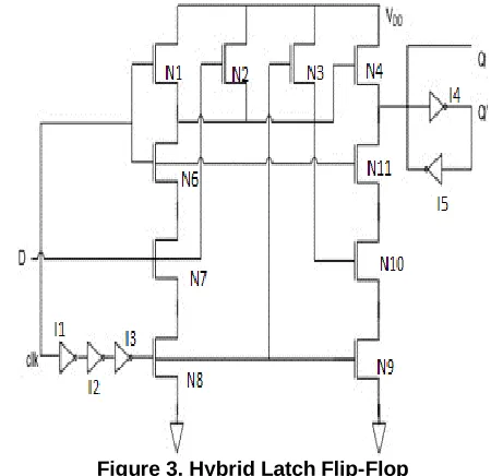
2.2. HYBRID LATCH FLIP-FLOP (HLFF)
The Hybrid Latch Flip-Flop is a high performance Flip-Flop introduces new mechanism of performing flip-flop functionality based on generating explicit transparency window where the transition is allowed. This approach greatly reduces the complexity of the locking mechanism results in small delay and small area. The hybrid latch flip-flop falls under hybrid category which has impressive delay property and can have negative setup time. HLFF is a static, single edge-triggered FF where it consumes more power. Existence of redundant transition in internal node in HLFF indicates more power consumption. It is similar to latch because it can provide a soft clock edge which allows for slack passing and minimize the effect of clock skew on cycle time. The circuit diagram of HLFF is shown in the figure 2.
Figure 3. Hybrid Latch Flip-Flop
This structure is basically a level sensitive latch which is clocked with an internally generated sharp pulse. This sharp pulse is generated at the positive edge of the clock using clock and delayed version of clock. Transistor level implementation of this flip-flop is given in above diagram. The number of transistors in HLFF logic is greater, and the existence of one to one glitch leads to wasting of power. HLFF has very simple structure but the unnecessary internal transition increase the total power consumption of flip-flop. Every time, the input is high a glitch is generated, regardless of previous state of the output Furthermore, the transistors in stack degrade the performance of the logic. The major advantage of this structure is its soft-edge property, i.e., its robustness to clock skew. One of the major drawbacks of the hybrid design in general is the positive hold time Hence we are going for the Modified Version of Hybrid Latch Flip-Flop. It is not suitable for low power application, since its power consumption limits its utilization.
2.3. MODIFIED VERSION OF HYBRID LATCH FLIP-FLOP
The Modified Version of Hybrid Latch Flip-Flop is also falls under the hybrid category of flip flop that has impressive delay property and can have negative setup time. This Modified Hybrid Latch Flip-Flop is a latch with brief transparency period. This is modified version of HLFF flip flop that has Lower number of transistors as well as less power consumption.
2.3.1. OPERATION OF MHLFF
142 Figure 4.Modified Version of Hybrid Latch Flip-Flop
Compared to HLFF the internal node transition in MHLFF occurs only when input has different logic values in two successive clocks. Signal clock is shifted in time (equal to delay of inverter chain) to generate clock BD. Depending on the state of input, node x is charged to Vdd or remains at low state. Suppose that D has high logic value, at rising edge of clock, node X is discharged through N1 and N3, hence Q is charged to Vdd and remains high during the clock period. Hence P1 will be OFF. If D has high value in the next rising edge of the clock, in contrary to previous logic, there is no transition in X, thus the extra power consumption is avoided. Compared to HLFF, the state of flip-flop is used to keep the state of internal node until input condition is changed. The number of transistors in the stack in this structure is less than that in HLFF, so the MHLFF is faster than HLFF. The lower power consumption of MHLFF with improvement in delay and area compare to others makes this logic so interesting. When clock pulse is 0 and data is 0, P2 transistor will be ON and it passes the complement value of clock that is 1 to transistor N3 which is turned ON that passes the value 0 to the above stage. The transistor N1 is turned OFF since the data is 0.where as the transistor P1 is turned OFF hence the node X will be 1. And the transistor N2 is ON the output will be 0. When clock pulse is 0 and data is 1, P2 transistor will be ON and it passes the complement value of clock that is 1 to transistor N3 which is turned ON that passes the value 0 to the above stage. The transistor N1 is turned ON since the data is 0.where as the transistor P1 is turned OFF hence the node X will be 0. And the transistor N2 is ON the output is 1. This design eliminates the unnecessary switching problems.Larger transistors N3 and N4 are required to be enhance the discharging of power Capability. Another drawback of this design is that node becomes floating when output Q and input Data both equal to ―1‖. Extra DC power emerges if node X is drifted from an intact ―1‖.
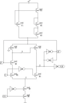
2.4. SINGLE ENDED CONDITIONAL CAPTURING ENERGY RECOVERY
Single Ended Conditional Capturing Energy Recovery Flip-Flop is one kind of Energy Recovery Flip-Flip-Flop. Where Energy Recovery is a technique developed for low power digital circuits, the energy recovery circuit achieves low energy dissipation by restricting current to flow across device with low voltage drop and by recycling the energy stored on their capacitors by using an AC type supply voltage. This SCCER Flip-Flop uses the Conditional Discharge Technique.
2.4.1. OPERATION OF SCCER
SCCER is the refined Low power pulse triggered flip-flop the circuit diagram of SCCER is shown in the below figure 5.This SCCER Flip-Flop uses the Conditional Discharge Technique. In this technique, the extra switching activity is eliminated by controlling the discharge path when the input is stable HIGH and thus the name conditional discharge technique. In this scheme, an NMOS transistor controlled by QB is inserted in the discharge path of the stage with high switching activity. When the input undergoes a Low-to-High transition the output Q changes to high and QB to low. This transition at the output switches off the discharge path of the first stage to prevent it from discharging. In this design, a weak pull up transistor P1 is employed in conjunction with an inverter I2 to reduce the load capacitance of node. The discharge path contains NMOS transistors N2 and N1 connected in series. In order to eliminate superfluous switching at node X, an extra NMOS transistor N3 is employed. Since N3 is controlled by Q_fdbk, no discharge occurs if input data remains high.
Figure 5.Circuit diagram of SCCER
143
3. SCCER WITH SELF CONTROLLABLE
VOLTAGE LEVEL CIRCUIT LOGIC (SVL)
The SVL circuit can reduce stand by leakage power of CMOS logic circuits with minimal overheads in terms of chip area and speed. In the operating Mode, it provides high-Speed Operation for load circuits. In the Stand-by Mode it provides, minimum Stand-by power, data retentions and high noise immunity.
Figure 6 .Circuit Diagram for SCCER with SVL logic
The SVL logic is added to the upper part and the lower part of the modified SCCER circuit.The modified SCCER circuit is decreased in transistor count when compared to figure 6.
3.1. SCCER WITH SELF-ADJUSTABLE VOLTAGE LEVEL CIRCUIT (SAL) LOGIC
It’s important to reduce the leakage power in all portable systems. Self-adjustable voltage level logic is a technique which is used for reducing leakage power in the circuit [13].
Figure6 .Circuit Diagram for SCCER with SAL logic
In the figure 6. the SAL logic is added on the top most part of the modified SCCER circuit and the circuit behaves as D flip-flop.
4. SIMULATION RESULTS
4.1. SIMULATION RESULT FOR ip-DCO The waveform of ip-DCO is shown in the figure 6.
Figure 6.Waveform of ip-DCO
4.2. SIMULATION RESULT FOR MHLFF The waveform of MHLFF is shown in the figure 7.
Figure7. Waveform of MHLFF
4.3. SIMULATION RESULT FOR SCCER The waveform of SCCER is shown in the figure 8.
Figure 8.waveform of SCCER
4.4.SIMULATION RESULT FOR SVL LOGIC WITH SCCER MODIFIED CIRCUIT
144 Figure 9. Waveform of SVL logic
4.5.SIMULATION RESULTS FOR SAL LOGIC WITH SCCER MODIFIED CIRCUIT
The waveform for SAL logic is given in figure 11
Figure 10.waveform of SAL logic
The figures 6,7,8,9,10 are the simulation results of ip-DCO,MHLFF,SCCER , and the modified circuit of SCCER with SVL and SAL logic. The simulation results shows that the flip-flop acts like a D-flip-flip-flop .
5. POWER COMPARISON TABLE
The power comparison table is given in table 11.
Figure11. Power comparison Table
6. POWER COMPARISON CHART
The power comparison is done between SCCER , SCCER with PTL logic, SAL and SVL techniques are designed. The power comparison chart is given in figure 12.
Figure 12.Power comparison chart
7. CONCLUSION
In this paper, the various Flip flop design like ip-DCO, MHLFF, SCCER and Proposed flip-flop design with pulse control scheme modified SCCER with SVL and SAL logics are discussed. These flip-flop were been designed in Tanner tool and the results and waveforms are also obtained. The comparison table also added to verify the designed methods. Even though, when the circuit is in idle condition the circuit consumer some power which is said to be leakage power. Simulation results indicate that the proposed design excels in performance indexes such as power and area. It is more efficient and comparatively it produces high performance results.
8. ACKNOWLEDGEMENT
We thank to Dr.P.Ramamoorthi,Prof.S.Arumugam, Prof. B.Devi of the VLSI Division, SNS College of Techology, Coimbatore,for their contribution of this work.
9. REFERENCES
[1]. H. Kawaguchi and T. Sakurai, ―A reduced clock-swing flip-flop(RCSFF) for 63% power reduction,‖ IEEE J.
Solid-State Circuits, vol.33, no. 5, pp. 807–811, May
1998.
[2]. A. G. M. Strollo, D. De Caro, E. Napoli, and N. Petra, ―A novel highspeed sense-amplifier-based flip-flop,‖
IEEE Trans. Very Large ScaleIntegr. (VLSI) Syst., vol.
13, no. 11, pp. 1266–1274, Nov. 2005.
[3]. H. Partovi, R. Burd, U. Salim, F.Weber, L. DiGregorio, and D. Draper,―Flow-through latch and edge-triggered flip-flop hybrid elements,‖ inIEEE Tech. Dig. ISSCC, 1996, pp. 138–139.
[4]. B. Kong, S. Kim, and Y. Jun, ―Conditional-capture flip-flop for statisticalpower reduction,‖ IEEE J. Solid-State
Circuits, vol. 36, no. 8, pp.1263–1271, Aug. 2001.
[5]. N. Nedovic, M. Aleksic, and V. G. Oklobdzija, ―Conditional prechargetechniques for power-efficient dual-edge clocking,‖ in Proc. Int. Symp.Low-Power
P-FF SCCE R
SCCER WITH SAL
LOGIC
SCCER WITH SVL LOGIC
Number of
transistors 17 11 15
Average Power (mWatts)
0.4718 0.4718 0.2359
MaxPower
(mWatts) 0.2773 0.0008 0.00014
Min.Power
145
Electron. Design, Monterey, CA, Aug. 12–14, 2002,
pp.56–59.
[6]. P. Zhao, T. Darwish, and M. Bayoumi, ―High-performance and low power conditional discharge flip-flop,‖ IEEE Trans. Very Large ScaleIntegr. (VLSI)
Syst., vol. 12, no. 5, pp. 477–484, May 2004.
[7]. C. K. Teh, M. Hamada, T. Fujita, H. Hara, N. Ikumi, and Y. Oowaki,―Conditional data mapping flip-flops for low-power and high-performancesystems,‖ IEEE
Trans. Very Large Scale Integr. (VLSI) Systems,vol.
14, pp. 1379–1383, Dec. 2006.
[8]. S. H. Rasouli, A. Khademzadeh, A. Afzali-Kusha, and M. Nourani,―Lowpower single- and double-edge-triggered flip-flops for high speedapplications,‖ Proc.
Inst. Electr. Eng.—Circuits Devices Syst., vol. 152,no.
2, pp. 118–122, Apr. 2005.
[9]. H. Mahmoodi, V. Tirumalashetty, M. Cooke, and K. Roy, ―Ultra lowpower clocking scheme using energy recovery and clock gating,‖ IEEETrans. Very Large
Scale Integr. (VLSI) Syst., vol. 17, pp. 33–44,
Jan.2009.
[10]. P. Zhao, J. McNeely, W. Kaung, N. Wang, and Z. Wang, ―Design osequential elements for low power clocking system,‖ IEEE Trans. VeryLarge Scale
Integr. (VLSI) Syst., to be published.
[11]. Y.-H. Shu, S. Tenqchen, M.-C. Sun, and W.-S. Feng, ―XNOR-baseddouble-edge-triggered flip-flop for two-phase pipelines,‖ IEEE Trans.Circuits Syst. II, Exp.
Briefs, vol. 53, no. 2, pp. 138–142, Feb. 2006.