J. Sens. Sens. Syst., 2, 127–135, 2013 www.j-sens-sens-syst.net/2/127/2013/ doi:10.5194/jsss-2-127-2013
©Author(s) 2013. CC Attribution 3.0 License.
RGB
Geoscientific Instrumentation Methods and Data Systems
Discussions
Geoscientific Instrumentation Methods and Data Systems
Open Access
Web Ecology
Open Access
Open
Access
JSSS
Journal of Sensors and Sensor SystemsPolymer composite based microbolometers
A. Nocke
Solid-State Electronics Laboratory, Technische Universität Dresden, Dresden, Germany
now at: Institute of Textile Machinery and High Performance Material Technology, Technische Universität Dresden, Dresden, Germany
Correspondence to: A. Nocke ([email protected])
Received: 12 February 2013 – Revised: 3 May 2013 – Accepted: 1 July 2013 – Published: 1 August 2013
Abstract. This work focuses on the basic suitability assessment of polymeric materials and the correspond-ing technological methods for the production of infrared (micro-) bolometer arrays. The sensitive layer of the microbolometer arrays in question is composed of an electrically conductive polymer composite. Semi-conducting tellurium and vanadium dioxide, as well as metallic silver, are evaluated concerning their suit-ability as conductive filling agents. The composites with the semi-conducting filling agents display the higher temperature dependence of electrical resistance, while the silver composites exhibit better noise performance. The particle alignment – homogeneous and chain-shaped alike – within the polymer matrix is characterized regarding the composites’ electrical properties. For the production of microbolometer arrays, a technology chain is introduced based on established coat-forming and structuring standard technologies from the field of polymer processing, which are suitable for the manufacture of a number of parallel structures. To realize the necessary thermal isolation of the sensitive area, all pixels are realized as self-supporting structures by means of the sacrificial layer method. Exemplarily, 2×2 arrays with the three filling agents were manufactured. The resulting sensor responsivities lie in the range of conventional microbolometers. Currently, the comparatively poor thermal isolation of the pixels and the high noise levels are limiting sensor quality. For the microbolome-ters produced, the thermal resolution limit referring to the temperature of the object to be detected (NETD) has been measured at 6.7 K in the superior sensitive composite layer filled with silver particles.
1 Introduction
Microbolometers belong to the group of thermal infrared de-tectors and are used as sensor arrays primarily in thermal imaging devices. In accordance with Planck’s law, the mea-suring of infrared radiation permits passive target analysis as well as non-contact temperature measurements of solid bod-ies, thus opening a large number of possible applications. In microbolometer detectors, the absorbed infrared radia-tion causes a change in temperature, triggering a local alter-ation in resistance within the sensitive area (thermoresistive effect). Conventionally, sensitive resistor elements include vanadium oxide (VOx), amorphous silicon (a:Si) and ceramic semiconductors (YBCO), which are not usually used in semi-conductor production and are difficult to deposit (Ambrosio et al., 2010). Additionally, such microbolometer arrays are manufactured in an elaborate technological process chain, as
individual pixels have to be realized as self-supporting struc-tures. This is necessary to ensure a high thermal insulation of the sensitive area and thus great thermal and electrical re-sponsivity. The high cost of microbolometer production is still limiting their widespread use, particularly civilian use, which is highly price-dependent. This motivates the basic re-search of alternative, economically viable materials and the corresponding technical methods for the production of mi-crobolometer arrays.
16 1
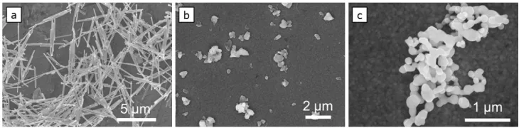
Figure 1. Scanning electron microscope (SEM) views of (a) synthesized tellurium needles, (b) 2
vanadium dioxide particles, and (c) silver particles. 3
Figure 1.Scanning electron microscope (SEM) views of (a) synthesized tellurium needles, (b) vanadium dioxide particles, and (c) silver particles.
layers (Kaufmann et al., 1996). The electrical properties of the modified polymer layer depend on the ion dose, the ion energy and the ion current density. Liger et al. describe an approach in which the sensitive layer is formed by pyrolyz-ing the parylene C polymer (Liger, 2006). The pyrolysis of the pre-deposited parylene layer is performed in two stages at temperatures ranging from 660 to 800◦C and causes a share of the benzene rings contained in the parylene C (Liger, 2006) to transform into graphite-like areas. The resistance of the pixel is determined by the rate of graphitization, and thus by the temperature during pyrolysis. Liger (2006) gives a calculated noise equivalent temperature difference (NETD) value for his microbolometer pixels of 31–109 mK. In these works, polymer-based technologies for the manufacture of self-supporting bolometer-pixels are presented. The consid-erable energy inputs required for the manufacturing methods described limits the application spectrum, particularly with regards to flexible polymeric substrates. Additional works, addressing in particular the production and characterization of polymer-based sensitive bolometer layers, examine the suitability of the intrinsically conductive polymer Poly(3,4-ethylenedioxythiophene)/Poly(styrenesulfonate) (Son et al., 2009) and of carbon nanotubes with (Aliev, 2008) and with-out (Zeng et al., 2012) surrounding matrix polymer. Best sensor performance for these sensitive materials is given by Zeng et al. (2012) with a calculated detectivity D∗ of 1.09×107cm Hz1/2W−1.
In this work, sensitive layers consisting of electrically con-ductive polymer composites composed of an insulating ma-trix polymer and a conductive filling material are used. When using such polymer composites, the mechanical, chemical and electrical properties of an individual layer can be ad-justed and optimized separately. Especially chemical and thus technological properties are determined by the polymer matrix, as long as the proportion of the filling agent is small enough. The electrical properties are given by the type, struc-ture and distribution of the conductive filling material.
2 Experimental
2.1 Materials
When selecting the materials to be used, the essential tech-nological and electrical requirements of the polymer-based microbolometer arrays have to be taken into account. For the sensitive polymer composites, individual conditions apply for both the polymer matrix and the filling agents. Further-more, both components have to be chemically compatible in order to form a stable suspension at least for the duration of processing.
2.1.1 Filling materials
Crucial criteria for material choice are the electrical param-eters resistivity and temperature coefficientαRof resistance. Semiconducting materials with a comparatively highαR of
−(2–5) % K−1 as well as metallic materials with exception-ally good noise performance show great potential as filling materials. Another requirement results from the individual pixel element’s geometry given by the sensitive layer’s max-imum layer thickness, which should be as small as possible (<2µm) to achieve the required low heat capacity of the mi-crobolometer pixel. Therefore, only sufficiently small filling particles, which are also synthesizable in the desired geomet-ric form while still meeting high quality standards, can be used. Considering these criteria, particles composed of tel-lurium (Te), vanadium dioxide (VO2) and silver (Ag) have been used within the framework of this research (Fig. 1).
Monocrystalline tellurium is a semiconductor with an anisotropic trigonal crystal structure, giving it a predominant growth direction along the main axis, with the tellurium par-ticles growing as needles. Another effect of its anisotropic structure is an anisotropic behavior of electrical conductiv-ity, which isσc=2 S cm−1along the main axis at room tem-perature, while being lower by magnitudes along the other axes (Nussbaum, 1954). Te-needles were synthesized using chemical reduction of telluric acid (H6TeO6) with hydrazine (N2H4) as presented by Mayers and Xia (2002). The chosen synthesis procedure leads to a clean surface of the particles, which is desired for good electrical contacts. The resulting tellurium needles display a homogeneous size distribution at
A. Nocke: Polymer composite based microbolometers 129
Table 1.Electrical properties of the examined materials at room temperature (300 K): band gap Eg; temperature coefficientαRof resistance and resistivityρ.
Material Eg[eV] αR[% K−1] ρ[Ωcm] Reference
Te (c axis) 0.33 −2.45 2.0 Loferski (1954)
VO2 0.65 −4.19 ≈100 Berglund and Guggenheim (1969)
Ag – 0.41 1.5×10⁻⁶ Ashcroft and Mermin (2001)
diameters of 200–250 nm and length of 5–6µm. The parti-cles’ aspect ratio, therefore, is ca. 25.
Polycrystalline vanadium dioxide particles with a size dis-tribution from a few hundred nanometers to ca. 10µm are commercially acquired with a purity of 99.9 % based on trace metals analysis, according to manufacturer information (manufacturer: Aldrich). By means of a sedimentation pro-cess, particles are separated depending on their size. The re-sulting particles have a maximum size of 2µm, as can be seen in Fig. 1b), and thus meet the above-mentioned geometrical requirements of filling material.
The silver particles used (manufacturer: Aldrich) were also acquired commercially and have a silver content of at least 99 % and a diameter of ca. 150 nm, according to manu-facturer information. The particles have a high defect struc-ture and internal energy, causing a metastable, energetic, ac-tivated powder, which may form agglomerates of a size of approximately 1–2µm.
The electrical properties of these materials are summa-rized in Table 1.
2.1.2 Polymers
The aspired requirement of realizing the individual sensor structures with just a few simple process steps is most easily attained by using filled photoresists. The structure transfer is performed by UV exposure through a photomask. The re-spective process step is reproducible and applicable in large scale. Furthermore, many photoresists can be cross-linked, making them chemically stable against solvents and giving them higher mechanical solidity. The cross-linking reaction takes place either directly under UV exposure or by subse-quent heat input.
One photoresist with the above-named properties is the AZ 1514 positive photoresist by Clariant, with the polymeric main component being Novolak. This photoresist is used as the polymer matrix of the microbolometer pixel’s sensi-tive layer. The special suitability of the AZ 1514 photoresist stems from its capability to be thermally cross-linked into a phenolic resin in the temperature range 120–160◦C after its lithographic structuring (Roy et al., 2003), which gives it ex-tremely stable mechanical and chemical properties.
Another structuring polymer used is the Pyralin 2722 pho-toresist by HD MicroSystems. It is a negative phopho-toresist with polyimide (PI) for its polymeric main component.
Poly-17 1
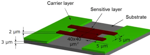
Figure 2. Geometric target parameters for the microbolometer pixel to be realized. 2 Figure 2.to be realized.Geometric target parameters for the microbolometer pixel
imides are very stable against most solvents and high tem-perature strains (>300◦C) (Fukukawa and Ueda, 2008) and therefore suitable for use as permanent, structuring carrier layers, which are created in the first process step of the mi-crobolometer array manufacture.
Other polymers used in this work are the heat-cured two-component Sylgard 184 (manufacturer: Dow Corning), with the silicone polydimethylsiloxane (PDMS) being the main component, and a paraffin wax purchased from Aldrich, with a melting range of 70–80◦C.
2.2 Technology
A technology chain was developed for the production of mi-crobolometer arrays whose sensitive layers are made from electrically conductive polymer composites. As the thermal insulation of the sensitive area is key, any pixels have to be re-alized as self-supporting structures. The construction scheme of a self-supporting pixel is portrayed in Fig. 2.
For the cost-effective production of microbolometer ar-rays, established coating and structuring standard technolo-gies for polymer processing were used, all of which are suit-able for the simultaneous creation of several structures. In particular, the following aspects had to be considered for these polymer technologies:
– It is necessary that the individual polymer layers can be
coated homogeneously in the desired thickness range, and easily structured laterally.
– The solvents and developers to be used must not
dis-solve or macerate the previously produced layers.
– The thermal stability of existent polymer layers has to
18
2
Figure 3. Schematic portrayal of the individual process steps for the manufacture of
3
microbolometer arrays under principal use of polymeric materials and technologies; UV ..
4
ultraviolet, PDMS .. polydimethylsiloxane.
5
6
Figure 3.Schematic portrayal of the individual process steps for the manufacture of microbolometer arrays under principal use of polymeric materials and technologies; UV – ultraviolet, PDMS – polydimethylsiloxane.
in the coating of inorganic materials (e.g., the deposition of electrodes).
The derived technology chain consists of seven elementary process steps (Fig. 3). Additional information can be found in Nocke (2011). The technological process is based primar-ily on the sacrificial layer technology, in which the sacrifi-cial layer is removed during the final process step, creating the self-supporting structure. The micromolding in capillar-ies (MIMIC) stamping technology was chosen for layer for-mation and simultaneous structuring of the sacrificial layer (Moonen et al., 2012). The sacrificial layer of heated, liquid paraffin wax fills a pre-structured channel network, owing to capillary action. Due to its low surface tension and viscos-ity, molten paraffin wax is particularly suitable for this struc-turing process. Furthermore, it displays favorable solubility properties, as it is only soluble in alkanes and few other sol-vents. Therefore, it barely limits the choice of possible or-ganic materials in the next process steps.
The electrically conductive networks in the sensitive poly-mer composites are realized by means of a dielectrophoretic alignment of the filling particles. This effect is based on the particles’ polarization in electrical fields and the resulting electrostatic force. In inhomogeneous electrical fields and under suitable conditions, the resultant force causes the de-sired formation of particle chains between the field-forming electrodes (Pohl et al., 1978; Nocke et al., 2009). The aim of such an alignment is the creation of a conductive network between appropriate electrodes at a preferably low filler load-ing (here: 0.1 wt. % in relation to the polymer matrix), which is essential for a technological malleability of the polymer composite.
2.3 Characterization
Electrical measurements were performed using the Elec-trometer 617 with the testbox 8002A (manufacturer: Keith-ley), which is well suited for high ohmic samples. For temperature-dependent measurements, a climate chamber HC0020 (manufacturer: Voetsch) with additional humidity control was used. All measurements were performed at 0 % relative humidity to minimize humidity influence. Noise and responsivity characteristics were measured with the lock-in amplifier 7265 DSP (manufacturer: EG&G Instruments). In order to establish the sensor parameters of a microbolome-ter pixel, the frequency-dependent responsivity RVwas mea-sured metrologically by detecting the voltage response of a modulated IR radiation source (manufacturer: DIAS infrared system CS 500 with chopper wheel) with the lock-in ampli-fier 7265 DSP. The measurement was performed in an evac-uated measuring chamber at an ambient pressure lower than 10 Pa.
3 Results and discussion
The main quality parameters of a microbolometer are the (voltage) responsivity RV, the detectivity D∗ and the noise equivalent temperature difference (NETD) (Gerlach and Budzier, 2010). The responsivity of a sensor is defined by the change in its output in proportion to the change of the in-put parameter and therefore should preferably be high. For a microbolometer, these parameters are the output voltage UO and the radiation fluxΦS, respectively. According to the re-lation
RV=dUO dΦS
= ααRUB
Gth
q
1+ω2 sτ2th
(1)
A. Nocke: Polymer composite based microbolometers 131
19
a) b) 1
c) 2
Figure 4. (a) Temperature coefficient of resistance and (b) spectral noise voltage density 3
(measured at 52 Hz) and (c) influence on detectivity D* ∝ | | / of a 4
microbolometer, calculated according to equation (3) in dependence on the resistance R of the 5
examined polymer composites with homogenous particle distribution (hom.) and particles 6
aligned by dielectrophoresis (Dep.). 7
8
Figure 4.(a) Temperature coefficientαRof resistance and (b) spectral noise voltage density ˜uRn(measured at 52 Hz) and (c) influence on detectivity D∗∝ |α
R|UB/˜uRnof a microbolometer, calculated according to Eq. (3) in dependence on the resistance R of the examined polymer composites with homogenous particle distribution (hom.) and particles aligned by dielectrophoresis (Dep.).
1
Figure 5. Optical microscopic pictures of dielectrophoretically aligned particles between 2
electrodes: (a) tellurium needles, (b) vanadium dioxide, and (c) silver particles. 3
4
Figure 5.Optical microscopic pictures of dielectrophoretically aligned particles between electrodes: (a) tellurium needles, (b) vanadium dioxide, and (c) silver particles.
with
τth=Cth/Gth, (2)
the responsivity RVof a microbolometer depends on the ab-sorption coefficientα, on the temperature coefficientαR of resistance, on the bias voltage UB, on the thermal conduc-tance Gthbetween the sensitive area and the surrounding me-dia, on the heat capacity Cthof the microbolometer pixel, on the thermal time constantτth, and on the angular frequency
ωS. The detectivity D∗and the noise equivalent temperature difference (NETD) are sensor parameters typically used to characterize the overall sensor performance by taking into account its ratio of measurement and noise signal. The cor-responding basic relation is given by
D∗=
√
APRV ˜uRn
∝ 1
NETD, (3)
where ˜uRnis the spectral noise voltage density and APis the pixel size.
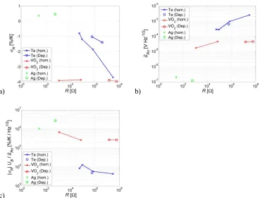
Figure 4 shows the relevant electrical properties of charac-teristic polymer composites for homogeneously distributed filling particles as well as for composites with particles aligned between the electrodes by dielectrophoresis (Fig. 5). Stemming from the temperature dependence of the resis-tance behavior (Fig. 4a) and additional measurements of the current-voltage characteristics (Nocke, 2011), the respective
21 1
2
Figure 6. Microscopic pictures of the polymer composite based microbolometers realized; 3
SEM-views of (a) the 2x2 array, and (b) a magnified individual pixel with a sensitive layer 4
containing aligned silver particles, view of the structures at a tilting angle of 75° across the 5
topview; optical microscopic pictures of individual pixels with aligned (c) tellurium needles, 6
(d) vanadium dioxide particles and (e) silver particles in the sensitive polymer composite. 7
8 9
Figure 6.Microscopic pictures of the polymer composite based microbolometers realized: SEM-views of (a) the 2×2 array, and (b) a magnified individual pixel with a sensitive layer containing aligned silver particles, view of the structures at a tilting angle of 75◦across the top view; optical microscopic pictures of individual pixels with aligned (c) tellurium needles, (d) vanadium dioxide particles and (e) silver particles in the sensitive polymer composite.
composites could be connected to individual dominant con-duction mechanisms:
– In tellurium composites, the electric conductivity is
con-siderably influenced by potential barriers between the particles. The related hopping conductivity mechanism exhibits a characteristic exponential relation of the re-sistance R and its temperature coefficientαR(Mott and Davis, 1979).
– In vanadium oxide composites, the measured
temper-ature coefficient αR corresponds approximately with the value of the filling material, which is αR,VO2=
−4.19 % K−1. Therefore, the total conductivity of these composites is determined largely by the semiconducting properties of the vanadium dioxide.
– The electrical properties of silver composites are
char-acterized by the metallic conductivity mechanism of the particles, which exhibit a positive and, relative to amount, small temperature coefficient of resistance
αR,Agof 0.41 % K−1.
The noise spectra of all composites display significant 1/f dependence. The noise levels of silver composites are lower by magnitudes compared to those of composites with semi-conducting filling particles (Fig. 4b). The resulting influence on detectivity D∗(Fig. 4c) is greater than the differences in the temperature coefficient of resistance αR. The detected electrical behavior of the polymer composites has proven largely independent of the variety of particle distribution.
Microscopic pictures of the produced 2×2 microbolome-ter arrays with the dielectrophoretically aligned filling ma-terials tellurium needles, vanadium oxide and silver parti-cles are shown in Fig. 6. They verify that the technological
22
1
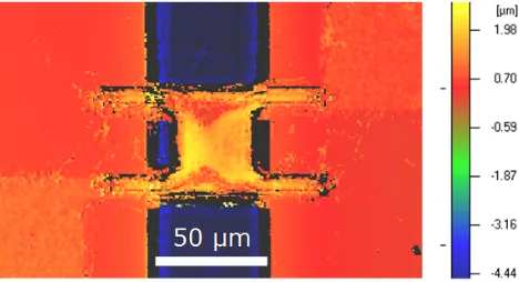
Figure 7. Confocal microscopic view of the surface topography of a microbolometer pixel
2
with a sensitive layer containing aligned tellurium needles.
3
4
Figure 7.Confocal microscopic view of the surface topography of a microbolometer pixel with a sensitive layer containing aligned tellurium needles.
process is reproducible, independent of the filling material used. The square pixel surface approximately conforms to the specified measurements of 40×40µm2. Figure 6a and b shows tilted scanning electron microscope (SEM) pictures of the microbolometer pixels filled with silver particles, prov-ing the self-supportprov-ing nature of these structures. The rough-ness of the contact arms is caused by diffraction effects oc-curring during the photolithographic process. The character-istics of the surface topography are examined in the example of a pixel with aligned tellurium needles (Fig. 7). The pixel has the desired layer thickness of 2µm and runs above the trench without significant bending. The trench has a depth of ca. 4.5µm.
Table 2 shows the application-relevant electrical and ther-mal sensor properties (see also Nocke, 2011). The relevant thermal parameters of the microbolometer arrays, thermal conductance Gth between the sensitive area, and the sur-rounding carrier layer and heat capacity Cth of the sensitive
A. Nocke: Polymer composite based microbolometers 133
Table 2.Electrical and thermal properties of realized polymer composite based microbolometers; calculation of sensor responsivities RVand detectivities D∗
according to the Eqs. (1) and (3); assumed absorption coefficientα=1.
Filling material Te needles VO2particles Ag particles
Bolometer resistance RB(293 K) [Ω]∗ 7.5±1.6×10⁶ 28±10×107 820±200
Temperature coefficientαRof resistance (293 K) [% K−1]∗ −1.4±0.1 −3.9±0.1 0.51±0.02
Bias voltage UB[V]∗ 9 9 0.5
Thermal conductance Gth[W K−1] 4.6×10⁻⁶ 4.6×10⁻⁶ 4.6×10⁻⁶
Heat capacity Cth[J K−1] 6.1×10⁻⁹ 6.1×10⁻⁹ 6.1×10⁻⁹
Thermal time constantτth[s] 1.3×10⁻³ 1.3×10⁻³ 1.3×10⁻³/1.1×10−4∗
Responsivity RV( f=50 Hz) [V W−1] 2.5×10⁴ 7.6×10⁴ 4.8×10²/2×102∗
Spectral noise voltage density ˜uRn 1.7×10⁻³ 8.1×10⁻⁵ 8.5×10⁻⁸
( f=50 Hz) [V Hz−1/2]∗ Detectivity D∗
( f=50 Hz) [cm Hz1/2W−1] 5.9×10⁴ 3.5×10⁶ 2.1×10⁷
NETD [K] (Nocke, 2011) 2.4×10³ 41 6.7
∗Measured values; statistical values refer to the four pixels of the respective array.
23
a) b)
1
Figure 8. (a) Measured responsivity
RV
and spectral noise voltage density
ũ
Rnand (b)
2
calculational derived detectivity
D*
for a microbolometer pixel with a sensitive polymer layer
3
containing dielectrophoretically aligned silver particles; bias voltage
UB
= 0.5 V, bolometer
4
resistance
RB
= 820
Ω
.
5
Figure 8.(a) Measured responsivity RVand spectral noise voltage density ˜uRnand (b) calculational derived detectivity D∗for a microbolome-ter pixel with a sensitive polymer layer containing dielectrophoretically aligned silver particles; bias voltage UB=0.5 V, bolometer resistance RB=820Ω.
layer are determined from the pixel dimensions and the re-spective material parameters. The calculated thermal param-eters results in a thermal time constant ofτth=1.3 ms. The responsivities RVof the produced microbolometer arrays are calculated according to Eq. (1), using the electrical param-eters of bolometer resistance RB, temperature coefficient of resistanceαR, and bias voltage UB determined in practice, as well as calculated thermal parameters. The responsivity values of the composites filled with tellurium and vanadium oxide filling materials are approximately two orders of mag-nitude above those of sensitive silver composites. This diff er-ence results from the smaller (according to amount) temper-ature coefficient of resistanceαRand the lower bias voltage UBfor the values with silver composite.
For the given similar geometric structures, the relation of the individual distinctive sensor parameters results from the electrical properties of the respective polymer composites shown in Fig. 4. Thus, the silver composites, due to their little noise behavior, have highest detectivity D∗and therefore the smallest NETD. The microbolometer arrays with vanadium
dioxide composites display the greatest responsivity RVdue to their high temperature coefficient of resistanceαR.
The sensor characteristics of a microbolometer pixel in terms of responsivity and spectral noise voltage density were measured exemplarily on a pixel structure filled with silver particles (Fig. 8a). At low frequencies, the detected respon-sivity is approximately frequency-independent with a value of ca. RV=2×10²V W−1. The distinct low-pass behavior sets in at a critical frequency of ca. 1.5 kHz, corresponding to a (thermal) time constant ofτth=0.11 ms. The subsequent detectivity of the measured pixel was calculated according to Eq. (3). As can be seen in Fig. 8b, it shows a strong frequency-dependence affected by the 1/f noise character-istic and the dynamic behavior of the responsivity.
While the measured responsivity is in a range comparable to the previously calculated one, the measured time constant is approximately one order of magnitude smaller than the cal-culated one (Table 2). The deviations can be traced back to erroneous estimates of thermal influences or the presumption
of an optimum wavelength-independent absorption coeffi -cient.
In comparison to values from the relevant literature, which places conventional microbolometers’ NETD values at around 30–100 mK (Gerlach and Budzier, 2010), funda-mentally higher NETD values were observed. One essential reason for this lies in the higher thermal conductances of the contact arms of the design presented here. Furthermore, the noise levels of polymer composites with semiconducting fill-ing particles are higher than those of semiconductfill-ing sen-sitive layers in conventional microbolometers. The same re-lation holds true with regards to the organic sensitive layer consisting of pyrolyzed parylene C (Liger, 2006). The NETD value comparison of microbolometers with metallic sensi-tive layers shows the smallest differences: NETD=500 mK (microbolometer with sensitive titanium layer: Mansi et al., 2003) as opposed to NETD=6.7 K (microbolometer pixel with silver composite). These metallic sensitive layers are distinguished by their very low noise levels.
4 Conclusions
The aim of this work was the basic suitability assessment of polymeric materials and related technological methods for the production of polymeric materials for the manufacture of microbolometer arrays with a sensitive layer of electri-cally conductive polymer composites. The all-polymer com-patible technology chain is an innovative approach to the manufacture of polymer-based, self-supporting MEMS (mi-croelectromechanical systems) structures and allows for a prospective economization potential as well as highly par-allel processing suitability. Concerning their suitability for use as sensitive layers in a microbolometer pixel, additional metrological and physical observations were made regarding the electrical properties of polymer composites filled with either tellurium needles, vanadium dioxide particles or silver particles.
The best noise equivalent temperature difference NETD, which is similar to the temperature-dependent resolution limit of the measuring object, was detected for the mi-crobolometer array with a sensitive silver composite layer, with its peak value at 6.7 K. This opens new applications for low-cost thermal imaging devices targeted at simple object detection.
In the future, the relevant sensor parameters have to be further improved in order to ensure a proliferation of possi-ble applications. This may be attained particularly well by an enhancement of thermal insulation of the individual pixels and a reduction of noise levels in the composites with semi-conducting filling particles. For a better thermal insulation of the individual pixels, the geometric properties of the con-tact arms have to be adapted to lower their thermal conduc-tance. This requires longer contact arms with a smaller cross section, which mechanically destabilizes the self-supporting
pixel structures. Thus, future inquiries will have to aim at fur-ther optimization of the polymer-based manufacturing pro-cess for microbolometer arrays described herein. Concerning the reduction of noise levels in the composites with semicon-ducting filling particles, the number and energetic height of potential barriers within the conductive network have to be reduced, as they are major factors in the noise behavior be-tween particles. One possible approach to this is to perform the chemical synthesis (of the sensitive semiconductors) in the vicinity of the microbolometer pixels themselves, lead-ing to barrier-free conductlead-ing paths with reduced bolome-ter resistances. An albolome-ternative is offered by depositing the thermoresistive layer in a separate step below or above the self-supporting polymer layer. With such a constructional ap-proach, the simple technology chain developed in this project could be used for the manufacture of self-supporting polymer layers. Thanks to the relevant photoresist’s great temperature stability for organic materials, conventional deposition meth-ods known from CMOS technology could be used, as appli-cable.
Acknowledgements. The author gratefully acknowledges financial support by the Saxon State Ministry of Science and Art and from German Research Foundation (DFG), Sonderforschungs-bereich 287.
Edited by: B. Jakoby
Reviewed by: three anonymous referees
References
Aliev, A. E.: Bolometric detector on the basis of single-wall carbon nanotube/polymer composite, Infrared Phys. Techn., 51, 541– 545, 2008.
Ambrosio, R., Moreno, M., Mireles Jr., J., Torres, and Kosarev, A.: An overview of uncooled infrared sensors technology based on amorphous silicon and silicon germanium alloys, Phys. Status Solidi C, 7, 1180–1183, 2010.
Ashcroft, N. W. and Mermin, N. D.: Festkörperphysik, Oldenbourg Verlag, München, 2001.
Berglund, C. N. and Guggenheim, H. J.: Electronic properties of VO2 near semiconductor-metal transition, Phys. Rev., 1, 1022– 1033, 1969.
Fukukawa, K.-I. and Ueda, M.: Recent progress of photosensitive polyimides, Polym. J., 40, 281–296, 2008.
Gerlach, G. and Budzier, H.: Thermische Infrarotsensoren: Grund-lagen für Anwender, Wiley-VCH, Weinheim, 2010.
Kaufmann, J., Moss, M. G., Wang, Y., and Giedd, R. E.: Conduc-tive polymer films for microbolometer applications, in: Infrared Technology and Applications XXII. SPIE 2744, Orlando, USA, 334–344, 1996.
Liger, M.: Uncooled carbon microbolometer imager, Dissertation (Ph.D.), California Institute of Technology, 2006.
Loferski, J. J.: Infrared optical properties of single crystals of tel-lurium, Phys. Rev., 93, 707–716, 1954.
Mansi, M. V., Brookfield, M., Porter, S. G., Edwards, I., Bold, B., Shannon, J., Lambkin, P., and Mathewson, A.: AUTHENTIC: a
A. Nocke: Polymer composite based microbolometers 135
very low-cost infrared detector and camera system, in: Infrared Technology and Applications XXVIII. SPIE 4820, Seattle, USA, 227–238, 2003.
Mayers, B. and Xia, Y. N.: One-dimensional nanostructures of trig-onal tellurium with various morphologies can be synthesized us-ing a solution-phase approach, J. Mater. Chem., 12, 1875–1881, 2002.
Moonen, P. F., Yakimets, I., and Huskens, J.: Fabrication of Tran-sistors on Flexible Substrates: from Mass-Printing to High-Resolution Alternative Lithography Strategies, Adv. Mater., 24, 5526–5541, 2012.
Mott, N. F. and Davis, E. A.: Electronic Processes in Non-Crystalline Materials, 2nd Edn., Clarendon Press, Oxford, 1979. Nocke, A.: Mikrobolometer auf der Basis von Polymerkompositen,
TUD Press, Dresden, 2011.
Nocke, A., Wolf, M., Budzier, H., Arndt, K.-F., and Gerlach, G.: Dielectrophoretic alignment of polymer compounds for thermal sensing, Sensor. Actuat. A-Phys., 156, 164–170, 2009.
Nussbaum, A.: Electrical properties of pure tellurium and tellurium-selenium alloys, Phys. Rev., 94, 337–342, 1954.
Pohl, H., Pollock, K., and Crane, J.: Dielectrophoretic force: A com-parison of theory and experiment, J. Biol. Phys., 6, 133–160, 1978.
Roy, D., Basu, P. K., Raghunathan, P., and Eswaran, S. V.: DNQ-novolac photoresists revisited: H-1 and C-13 NMR evidence for a novel photoreaction mechanism, Magn. Reson. Chem., 41, 84– 90, 2003.
Son, H. J., Kwon, I. W., and Lee, H. C.: Passivation
Effect for the Reduction of 1/f Noise in
Poly(3,4-ethylenedioxythiophene):Poly(styrene sulfonate) Thin Films Based on Uncooled Type Microbolometer Applications, Appl. Phys. Express, 2, 041501, 2009.