Abstract
In this paper, the design, operational principle and experimental validation of an endfire antenna element that is inspired by the energy-focusing characteristics of graded-index optical fibre are presented. The antenna operates with a bandwidth of 1.5 GHz centred around 14 GHz. It has a gain of around 5.5 dBi along the band of interest and a good pattern stability over the band. The antenna derives its unique nature from the arrangement of the arc-shaped parasitics, that couple onto the antenna´s driver dipole. An electromagnetic refractive index retrieval mechanism is used to guide the placement of the parasitics to enhance the gain. In addition to the design principle, a parametric study of the main parameters and their influence on the antenna behaviour is presented. The antenna is a potential candidate for use in multi-user massive MIMO antenna arrays for 5G communications where space is premium and in antenna array applications where a low-profile antenna element with a high gain is a necessity.
1 Introduction
Scenarios of high data-rate transmissions of several gigabits per second require the use of wide bandwidth and high directivity beams. The wide bandwidth is attained by shifting to a higher millimetre wave fre-quency, and to obtain high directivity beam, antennas need to be designed to focus the beam with high front-to-back (F/B) ratio. When employed in an array, such an antenna further enhances the directivity of-fered from the array. Recently there has been an in-creasing interest in the 14–15-GHz band [1–3]. A printed antenna configuration is attractive owing to the simplicity of manufacturing, scalability and the re-duced cost. The conventional patch or printed dipole antennas generally have a low directivity omnidirec-tional pattern. Among the techniques used to enhance this directivity, the use of parasitic elements coupled to the printed dipole is appealing. Accordingly, an endfire antenna element based on parasitics aided quasi-Yagi and fibre-optics principle is proposed in this paper. Following the analogy to the graded re-fractive index optical fibre energy-focusing principle, the designed antenna element has its gain and
directivity enhanced—mainly by a unique arrangement of parasitics around the driving sources, aided by reconfigured refractive index—referred to as quasi-optic approach.
Endfire antenna topologies such as the helical tenna, antipodal Vivaldi antenna and the Yagi-Uda an-tenna have been used in applications such as ultra-wideband, phased array, radars and microwave imaging. Printed endfire antenna elements have been used for high-gain applications. These are generally fed by a half wavelength resonant driver, and the coupling between the driver element and the director element is set to maximize the achievable gain. The compactness of res-onant type antennas and the broad bandwidth charac-teristics were both simultaneously achieved in a single Yagi antenna [4] where a microstrip to CPS transition balun was used to add to the profile length. With the compactness and broad bandwidth addressed by anten-nas in [4, 5], papers [6, 7] focus on improving the an-tenna gain using techniques of a microstrip-fed inset patch as the driver, with parasitic patches added as di-rectors to enhance the gain. The dipole feeding point in this antenna design is based upon [8], where the
an-tenna operates in the 2–4-GHz band with a gain of
around 5 dBi over the band. Since Yagi-Uda antennas or the endfire antennas in general are protrude-out-of-wall configurations, it adds immensely if this dimension of profile length could be minimized while retaining
© The Author(s). 2019Open AccessThis article is distributed under the terms of the Creative Commons Attribution 4.0 International License (http://creativecommons.org/licenses/by/4.0/), which permits unrestricted use, distribution, and reproduction in any medium, provided you give appropriate credit to the original author(s) and the source, provide a link to the Creative Commons license, and indicate if changes were made.
* Correspondence:[email protected]
1Department of Antennas, TTI Norte, Parque Científico y Tecnológico de
Cantabria, C/ Albert Einstein n° 14, 39011 Santander, Spain
2Departamento de Ingeniería de Comunicaciones, Universidad de Cantabria,
the high-gain characteristics. The novelty of the an-tenna that is presented in this paper is threefold: it of-fers the characteristics of [4–7], proposes a feeding structure to minimize the profile length and adds around 3 dBi to the gain of a basic Yagi antenna, by in-corporating a specific, variable refractive index-guided novel arrangement of arc-shaped parasitics, in front of
the driver dipole. This launches the surface waves in such a way as to aid their transformation into direc-tional far-field components. A prototype of the low-profile antenna element which measures a square centi-metre across has been fabricated and experimentally validated.
The rest of the paper is organized as follows: the an-tenna element design principle is introduced in Section 2, Section 3 discusses the antenna fabrication and ex-perimental validation of the antenna element with the measurement results and Section 4 concludes.
2 Antenna design principle
The design philosophy adopted rests on the use and integration of three basic elements that form the an-tenna design: the driver dipoles, the printed reflector and the parasitics. The antenna was brought into op-eration over an evolved sequential design following first the principles. In the following, the design is dis-cussed for each of the three constituent basic elements.
2.1 Driver dipoles
The substrate chosen for the printed antenna config-uration has a dielectric constant εr = 3.55, loss
tan-gent (tan δ) = 0.0027 and a thickness of 0.508 mm.
The substrate area was chosen to mitigate the sur-face waves and the fringing edge effects to a consid-erable extent by maintaining a peripheral distance between the structure to the boundaries greater than a quarter wavelength. The substrate area was thus
set to 12 mm × 11 mm. A λ/2 printed dipole centred
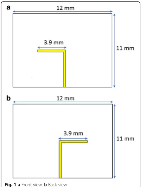
at the chosen frequency of 14 GHz was designed. The arms of the dipole were chosen to be printed Fig. 1aFront view.bBack view
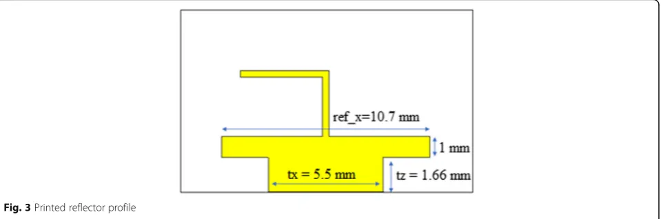
Fig. 3Printed reflector profile
Fig. 4Effect of the variation of ref_x on S11 frequency response
on opposite sides of the substrate to act as a
self-balancing structure. Figure 1a shows the front view
of the design of an arm of the dipole on the
sub-strate and Fig. 1b shows the back view of the other
arm. Initially, the length of each arm was selected as
λ0/4 at 14 GHz, equal to 5.35 mm. The length of the arm was later fine-tuned through full-wave simula-tions to 3.9 mm to have the band centred at 14 GHz. A parametric variation of the arm length and its
ef-fect on S11 is shown in Fig. 2. For this parametric
variation of other parameters such as the transition length and width, the reflector length and width are kept constant and only the arm length is varied in steps of 0.25 mm, displaying the tuning behaviour
over the 12–18 GHz range for an arm length vari-ation from 3 mm to 5.25 mm. This tuning behaviour demonstrates the potential of the antenna to be reconfigured in frequency.
2.2 The printed reflector
The antenna design requires a printed reflector to enhance the directivity and the front-to-back ratio. The design of the printed reflector is performed to use the reflector both as a ground and as a supporting structure to the SMA feeder connector. This requirement makes the reflector a stepped design with the width (tx) of the section facing the SMA near toλ0/4 at 14 GHz and equal to 5.5 mm. The actual Fig. 6Effect of the variation of tx (transition width) on cross-polar level for Phi90 plane
reflector length (ref_x) isλ0/2 at 14 GHz equal to 10.7 mm. The final printed reflector, which is printed on the face op-posite to the side where the SMA pin connects, is shown in Fig.3with its optimized dimensions.
A parametric study was performed over the transi-tion width (tx), transitransi-tion length (tz) and the
re-flector length (ref_x). As shown in Fig. 4, the
reflector length variation (ref_x) does not affect the frequency behaviour excessively. This strengthens the dependence of the frequency behaviour of the
an-tenna mainly on the arm length as shown in Fig. 2
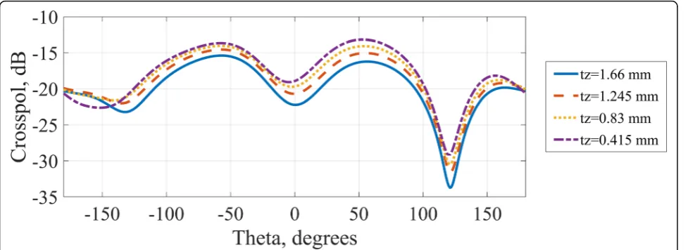
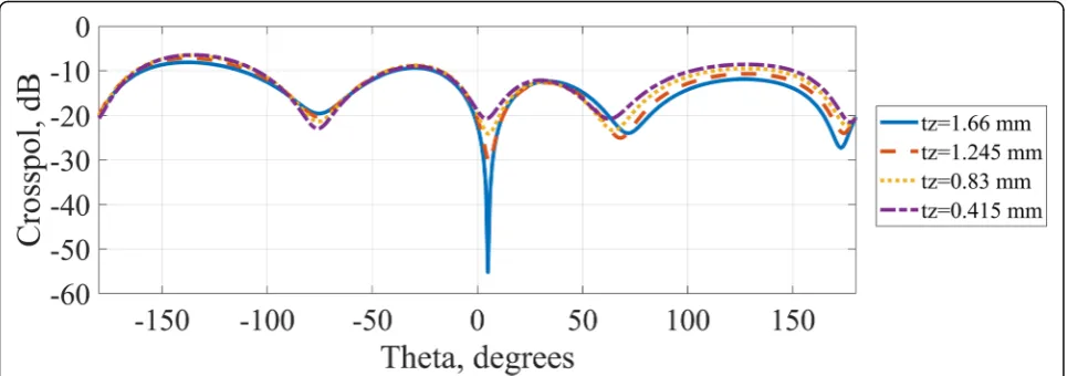
with the reflector aiding in enhancing the front-to-back ratio. A redesign of the reflector is needed for each tuning frequency. It was observed that the tran-sition dimensions affect the amount of realizable cross-polar levels. A parametric study of this de-pendence was performed by varying the transition length (tz) and transition width (tx) vs the observ-able cross-polar levels at Phi0 and Phi90 principal cut planes, and results are shown in Figs. 5, 6, 7 and 8. It was seen that the effect of varying the transi-tion width (tx) is not as pronounced as the effect of varying the transition length (tz). Variation of tz controls the observable cross-polar levels. As seen from Fig. 8, a substantial increase in the cross-polar levels is observed around boresight for variations over tz. The length before the transition step is a crucial factor that controls the cross-polar levels of the antenna and therefore has been deduced to be equal to 1.66 mm both by considering the surface
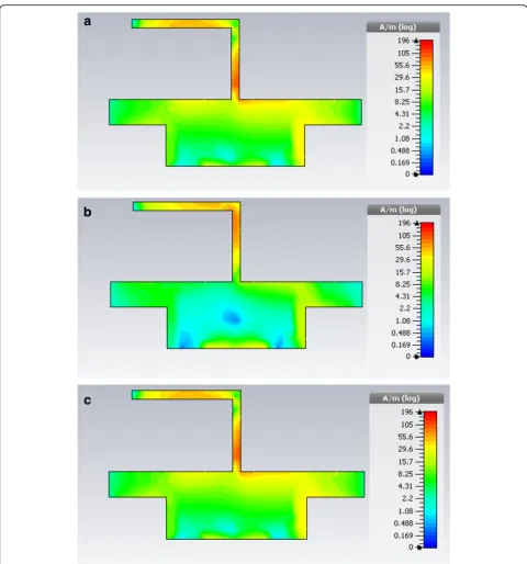
current distribution as shown in Fig. 9 and the
cross-polar levels of the pattern. Here the surface current distribution is stronger on the dipole arms for the depicted cases of absolute surface current phase of 0°, 90° and 180°, showing that the reflector performs the field enhancement through reflection.
The full-wave solver calculated values of the cross-polar levels after the full design of the antenna helps also in deciding the transition step length of tz = 1.66 mm and plays a critical role in the design.
2.3 The parasitics
In Fig. 9, the surface current distribution shows the currents strongly distributed on the dipole arms. It is intended to couple the electric field due to this onto the parasitics in a constructive way to enhance the far-field gain. To achieve this, a systematic dis-tribution of parasitics is proposed. The first parasitic that couples the dipole arm field is a
rectangle-shaped parasitic as shown in Fig. 10. The electric
field coupled onto this rectangle-shaped parasitic is distributed along two oblique directions, using two
symmetrically placed square parasitic elements,
whose dimensions are 0.05 λ × 0.05 λ that translates to 1 mm × 1 mm, each suitably spaced from each other to enhance coupling, while equally distributing the electric field along two symmetric oblique direc-tions. Figure 10 shows the rectangle-shaped parasitic and the two square parasitics coupling onto the di-pole. The capacitive coupling gap between them was set to maximize the coupling.
considered analogous to a certain cuboidal volume region, lying directly below the endfire central axis of the antenna, where the graded real refractive index is set to a maximum. The outward displace-ment towards the edges can be considered to repre-sent the cladding—where there is a gradient decrease of the real refractive index moving away from the centre. This is achieved by the methodical placement of the arc-shaped parasitics in front of the driver di-poles over the antenna plane. The procedure to ar-rive at this is discussed next.
The dielectric substrate used in the antenna can be considered a homogeneous slab for the frequencies under consideration. The refractive index is the re-configurable parameter that is used to direct the mechanism of radiation. Then according to [9], the general procedure for the retrieval of the material pa-rameters, in this case, the real part of the refractive index is as follows: the arc-shaped parasitics are placed so that they focus the electric field towards the boresight axis. A one-dimensional transfer matrix T relates the fields on one side of a slab to the other. For a homogeneous 1D slab, it takes the form (1):
T¼
where n is the refractive index, z is the wave imped-ance,kis the wave number anddis the thickness of the slab. A scattering matrix relates the impinging field amplitude to the outgoing field amplitude. The elements of the S matrix can be related to the elements of theT matrix as in (2) [10]:
For a homogeneous slab from equation (1),
T11 ¼T22¼TSand detð Þ ¼T 1
And theS matrix is symmetric. Using the information in equation (1), (3) and (4) can be derived:
S21¼S12 ¼ 1
Solving equations (3) and (4) for n and z yields (5) and (6) [9]:
The design principle of the antenna revolves mainly around equation (5) which gives the expres-sion for the refractive index as a function of the
re-flection and transmission S parameters and the slab
length d. The application of equation (5) is first per-formed over a single-unit cell of the arc-shaped
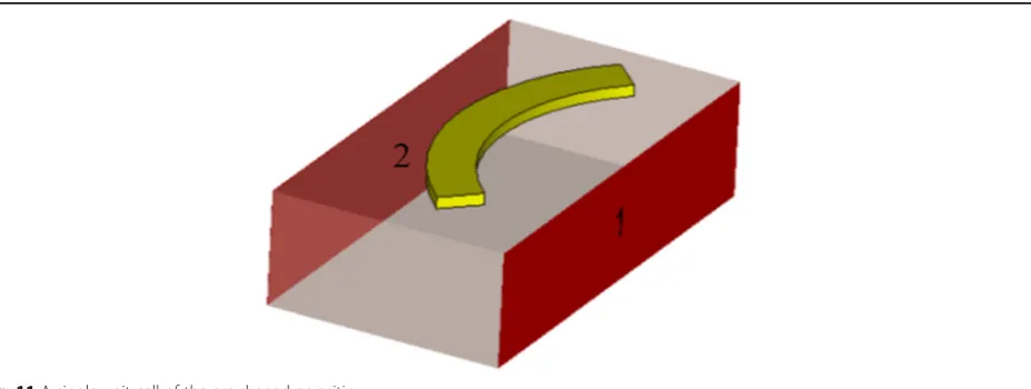
par-asitics (ASP) as shown in Fig. 11. The unit cell is
excited by waveguide ports excited on the two faces of the dielectric slab on which the ASP is printed. On running the simulation in a full-wave solver for the desired frequency of interest, the S11 and S21
values can be obtained. The length of the arc of the
ASP is 1.7 mm, around λ/10 at 14 GHz.
Of the total 10 ASPs selected to enhance the end-fire gain, five are on the left side of the endend-fire axis and the other five are symmetrically on to the other side. Equation (5) is used to calculate the refractive index as illustrated in Fig. 12 which depicts the way the refractive indices were calculated starting from the endfire central axis, towards the extreme left. Since the structure is symmetrical across the endfire axis, the same calculation of the refractive index holds for the right side as well.
structure is shown, with different curves signifying— the distance between the arc-shaped parasitic element and the square resonator (d)—1 mm being the closest one near to the central axis and 3 mm for the one on the extreme flaring edges. The imaginary part of the refractive index in these cases is near zero signifying minimum loss in radiating energies.
Fig. 10Rectangle-shaped parasitic and the two square parasitics coupling onto the dipole
Fig. 11A single-unit cell of the arc-shaped parasitic
energy towards the centre increasing the gain of the antenna. The simulation results of the antenna have been presented in [11].
2.4 Effect of antenna backplate
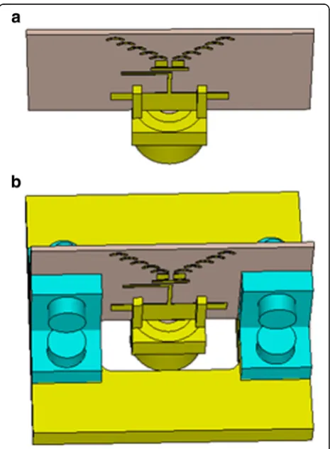
The antenna design described above in Sections 2.1, 2.2 and 2.3 is fed with a suitably designed 50-ohm coaxial SMA connector as in Fig. 15a. As the goal is to use the antenna in an array, a common mechanical support plate to connect and support multiple antenna elements is needed. The supporting plate is designed with a square hole in the centre as shown in Fig.15b. The pres-ence of the supporting plate with a hole has two func-tions: (1) It sufficiently isolates the ground of the designed antenna and maintains a purity in the tuning of the resonant frequency. (2) It enhances the obtained gain pattern by providing for improved cross polar levels. The 3D co-polar gain radiation pattern obtained out of
the antenna without the backplate and with the holed backplate is shown in Fig. 16. The 3D cross-polar gain pattern for the same two cases is shown in Fig.17.
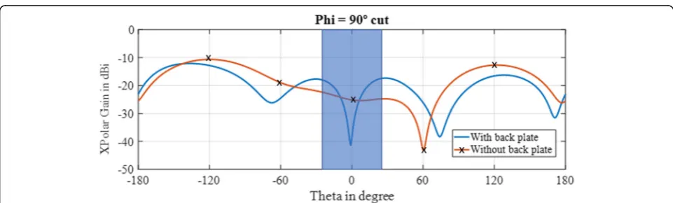
The cross-polar discrimination (XPD) improvement for the case with the backplate is compared with the case without and is shown in the Cartesian plot in Fig. 18. It can be clearly seen that the XPD is
im-proved considerably with the use of a holed
Fig. 13Real part of the refractive index of the unit cell parasitic arc-shaped resonators from centre towards edges
Fig. 14Gradient depiction of the gradient variation of the
Fig. 163D co-polar radiation pattern of the antenna.aWithout backplate.bWith backplate
Fig. 173D cross-polar radiation pattern of the antenna.aWithout backplate.bWith backplate
backplate by 15 dB along the boresight direction for a beamwidth of 20°.
3 Measurements and discussion
The designed antenna obtained by combining the
steps outlined in Section 2 is shown in Fig. 19 and
consists of a dipole driver element with arms printed
on opposite sides of the substrate and a printed re-flector to improve the forward radiation. A parasitic rectangular director couples the E-field into the two square parasitic elements that act as driving sources to the arrangement of the arc-shaped parasitic unit cell. These are flared in a V shape and spaced 0.2 mm from each other. The dimensions of the proposed quasi-Yagi antenna are shown in Fig. 19. The simula-tions were carried out in Ansoft HFSS. The antenna has an operational band from 13.5 to 15 GHz, with a
fractional bandwidth of 10.52%. The
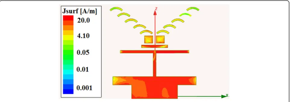
energy-channelling behaviour of the arc-shaped transitions is illustrated by the simulated current densities shown
in Fig. 20 at 14 GHz. To check the validity of the
Fig. 19Low-profile, high-gain quasi-Yagi antenna element dimensions.aFront view.bBack view
Fig. 20Surface current distribution at 14 GHz
proposed structure, a prototype was fabricated as
shown in Fig. 21 and measured in an anechoic
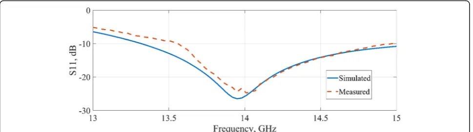
cham-ber. The simulated and measured S11 are compared
respectively by a blue line and red dashed lines in Fig. 22: a 10-dB return loss bandwidth of approxi-mately 1.5 GHz around 14 GHz is obtained. The printed antenna was backed by an aluminium sup-porting structure, with a square gap in the middle to allow for the SMA feeding and to enhance the XPD.
Besides, both the principal pattern cuts as well as boresight direction (0°) gain were measured in a far-field anechoic chamber, directly attaching the proto-type to the support plate of the roll over azimuth positioner, whose dimensions are much larger than the base of the fabricated prototype of Fig. 21. The
model of the support plate is shown in Fig. 23 to
give a comparison of the size. The simulated (blue dashed lines) and measured (red lines) radiation pat-terns for the co-polar component are compared in Figs. 24 and 25 for both principal planes, elevation and azimuth cuts, respectively. A slight asymmetry of the current distributions can be observed that ex-plains the approximately 20° deviation of the max-imum on the elevation cut shown by the red line on
Fig. 24 a. An almost symmetric response is obtained
in the azimuth cut shown in Fig. 24b. The large size of the supporting plate generates a reflected signal that adds to the prototype radiation causing an in-creased degradation of the measured patterns when departing from boresight (0°). Also, both the roll positioner and mast covered by absorbers block the measured signal on the back side which translates to Fig. 22Simulated and measuredS11behaviour of the antenna element operating from 13.5 GHz to 15 GHz for 10-dB return loss
minimum back lobes in the measured pattern as in
Fig. 24a and b. A reasonable agreement between
measurements and simulation patterns is obtained. Moreover, the gain of the antenna was measured using the two-antenna method for its variation over frequency. The simulated (blue dashed line) and measured (red line) gains in the boresight direction are compared in Fig. 26. A gain variation of 1 dB is seen in the band of interest that can be attributed to the ripple associated
4 Conclusion
A low-profile endfire antenna element inspired on
fibre-optic principles is presented. A
gradient-refractive index-based theoretical framework of the design, supported by parametric variation, is dis-cussed. The antenna prototype has been fabricated and experimentally validated. It has an operation over 1.5 GHz of bandwidth centred around 14 GHz with a directional high-gain radiation pattern. The inherent layered structure when incorporated in an array aids
to the better cooling of the antenna front end. The antenna element can find potential use in multi-user massive MIMO antenna arrays as well as in multi-beam switching antenna arrays for 5G. The prototype has been adopted in a massive MIMO array and its performance has been validated. These findings are presented in [12] dedicated to the design and imple-mentation of the massive MIMO array and its multi-beam characteristics. Moreover, a performance
evalu-ation of the fabricated antenna in a unique
reconfigurable array setup applied to practical scenar-ios using spatial modulation is presented in [13].
Abbreviations
5G:5th generation; ASP: Arc-shaped parasitic; CPS: Coplanar stripline; F/ B: Front-to-back ratio; HFSS: High-frequency structure simulator; MIMO: Multiple-input multiple-output; SMA: SubMiniature version A; XPD: Cross-polar discrimination
Authors’contribution
VB proposed the main idea, completed the experiments, analysed the results and wrote the paper. BB contributed in the pattern measurements. LC and JB read the paper and contributed critical constructive reviews. All authors read and approved the final manuscript.
Funding
This work was supported by the 5G wireless project that has received funding from the European Union’s Horizon 2020 research and innovation programme under grant agreement No. 641985.
Availability of data and materials
The data used in the analysis and validation of the proposed antenna was generated by measurements at the vector network analyser and the anechoic chamber. Though this data has been presented in the form of graphs in the paper, raw data is available on request from the corresponding author.
Competing interests
The authors declare that they have no competing interests.
Received: 17 October 2018 Accepted: 3 July 2019
References
1. "Ericsson 5G delivers 5 Gbps speeds”, Ericsson press release July 2014. Weblink: https://www.ericsson.com/en/press-releases/2014/7/ericsson-5g-delivers-5-gbps-speeds.
2. A Harada et al., 5G trials with major Global vendors. NTT Docomo Technical Journal, Special articles on 5G Technologies towards 2020 deployment, Volume 17, No. 4, April 2016.
3. P. Fleming,“5G research at Nokia networks”, 5G day at MIT wireless center, May 2015.
4. N. Kaneda, Y. Qian, and T. Itoh, A novel Yagi–Uda dipole array fed by a microstrip-to-CPS transition, inAsia–Pacific Microwave Conf. Dig., Yokohama, Japan, pp. 1413–1416, Dec. 1998.
5. W. R. Deal, N. Kaneda, J. Sor, Y. Qian and T. Itoh, A new quasi-Yagi antenna for planar active antenna arrays, inIEEE Transactions on Microwave Theory and Techniques, vol. 48, no. 6, pp. 910-918, Jun 2000.
6. G. R. DeJean and M. M. Tentzeris, A new high-gain microstrip Yagi array antenna with a high front-to-back (f/b) ratio for wlan and millimeter-wave
applications. inIEEE Transactions on Antennas and Propagation, vol. 55, no. 2, pp. 298-304, Feb. 2007.
7. G. R. DeJean, T. T. Thai, S. Nikolaou and M. M. Tentzeris, Design and analysis of microstrip bi-Yagi and quad-Yagi antenna arrays for WLAN applications. inIEEE Antennas and Wireless Propagation Letters, vol. 6, pp. 244-248, 2007. 8. J. Floc’h, A. Ahmad, Broadband QUASI-Yagi antenna for WiFi and WiMax
applications. Wirel. Eng. Technol.4(2), 87–91 (2013)
9. D. Smith, D. Vier, T. Koschny, and C. Soukoulis, Electromagnetic parameter retrieval from inhomogeneous metamaterials. Phys. Rev. E, vol. 71, pp. 036617(1-11), Mar. 2005.
10. D. M. Pozar. Microwave engineering. 4th Edition, Hoboken; John Wiley and Sons Inc., 2011.
11. V. Basavarajappa, B.B. Exposito, L. Cabria and J. Basterrechea, Millimeter wave multi-beam-switching antenna, inProc. IEEE International Symposium on Wireless Communication Systems (ISWCS), Bologna, Italy, 29-31 Aug. 2017. 12. V. Basavarajappa, B.B. Exposito, L. Cabria and J. Basterrechea, Binary phase
controlled multi-beam-switching antenna array for reconfigurable 5G applications. accepted for publication in this special issue of EURASIP JWCN. 13. D.N.Viet, M. D. Renzo, V. Basavarajappa, B. B. Exposito, J. Basterrechea and D.
T.P. Huy, Spatial modulation based on reconfigurable antennas: performance evaluation by using the prototype of a reconfigurable antenna. accepted for publication in this special issue of EURASIP JWCN.
Publisher’s Note
Springer Nature remains neutral with regard to jurisdictional claims in published maps and institutional affiliations.