ABSTRACT
DYCUS, JOSEPH HOUSTON. Advancing Atomic Scale Quantification of Interface Structure and Chemistry via Scanning Transmission Electron Microscopy. (Under the direction of James M. LeBeau.)
Electron microscopy is a powerful tool to characterize materials from the micro to
atomic scale. Scanning transmission electron microscopy (STEM) has become notably
important with resolution within the sub–˚Angstr¨om regime. Such resolution provides
information on the relationship between atomic structure and material properties. In
addition, breakthroughs in spectroscopy have provided elemental mapping of
individ-ual atom columns leading to information such as chemical segregation. Although STEM
is a powerful tool, its widespread use is relatively recent, leaving many opportunities
to employ STEM to discover new information in materials systems and develop
tech-niques to further advance capabilities of the instrument. In this work, the combination
of aberration–corrected STEM imaging and spectroscopy are employed to identify
rela-tionships between structure and chemistry in materials systems for interfaces and bulk
materials. Further, by building upon recently developed revolving STEM (RevSTEM),
a calibration scheme has been developed to reduce scan distortion in imaging, enabling
highly precise and accurate determination of atom column positions. Additionally,
path-ways for improving the signal–to–noise in energy dispersive X–ray mapping are shown.
By a combination highly accurate distance mapping and atomic scale EDS, important
materials relationships can be determined such as the effects of elemental segregation on
© Copyright 2017 by Joseph Houston Dycus
Advancing Atomic Scale Quantification of Interface
Structure and Chemistry via Scanning Transmission Electron Microscopy
by
Joseph Houston Dycus
A dissertation submitted to the Graduate Faculty of North Carolina State University
in partial fulfillment of the requirements for the Degree of
Doctor of Philosophy
Materials Science and Engineering
Raleigh, North Carolina
2017
APPROVED BY:
Elizabeth C. Dickey Douglas L. Irving
Brian J. Reich James M. LeBeau
DEDICATION
BIOGRAPHY
Houston Dycus was born in Knoxville, TN, where he lived until he finished his
under-graduate education at The University of Tennessee – Knoxville. During his Junior year
in High School, a strong link to science was formed when he was introduced to classical
mechanics and Newton’s Laws of Motion. The ability to model the trajectory of an
ob-ject with simple relationships sparked a curiosity of science that would ultimately propel
his own trajectory towards studying advanced courses in physics. At The University of
Tennessee - Knoxville, he was first introduced to the field of materials science. The direct
connection of the atomic arrangement of atoms and the behavior they exhibit compelled
him to dig deeper into the matter and find his way into the field of electron microscopy.
ACKNOWLEDGEMENTS
I would like to thank many people for all of their overwhelming support and
encourage-ment through my education. This work is not accomplished from my doing alone, rather
it is the culmination of many years of teaching and teamwork.
First I would like to thank my advisor Professor James Michael LeBeau. Thank you
for the countless hours of instruction and discussion as well as allowing me the freedom
to pursue many of my own ideas. I am also grateful for all of my committee members
for taking their time to provide input into my work. I would like to thank Professor
Elizabeth Dickey for being a fantastic teacher and providing the necessary knowledge of
crystallography and TEM I would need to succeed in research.
I would like to thank all of the Postdoctoral Scholars from the LeBeau group. Thank
you Dr. Xiahan Sang for helping me learn how to script and the tremendous help with
RevSTEM analysis. Thanks to Dr. Ryan White for training me on the Titan. Thanks
to Dr. Weizong Xu for help on several projects in the past few years. Also, Thanks to
Dr. Rohan Dhall for educating me on many details of low-loss EELS. In addition to the
Postdocs, I would like to thank all of my group members for their support and
encour-agement over the years: Dr. Adedakpo Adesoji Oni, Bahar Alipour, Everett Grimley,
Lindsay Hussey, Matthew Junior Cabral, Weiting Chen, and Jim Fitch. I would also like
to thank all of the staff at NC State’s Analytical Instrumentation Facility for keeping
ev-erything running as smoothly as possible and kindness with helping me learn how to use
the equipment. Thank you to all of my collaborators: Prof. Irving, Prof. Collazo, Prof.
Sitar at NCSU; Dr. Findlay and Dr. Allen at Monash and Melbourne; and Professor
Corral at University of Arizona. I would also like to acknowledge my financial support by
Beyond those directly involved in my research, I would like to express my graditude to
everyone in the other areas of my life. First, I cannot overstate the importance of having
such a supportive and caring family. Thank you Mom and Dad for raising me to be the
person I am today and allowing me the flexibility and freedom during my childhood to
develop skills in areas outside of the classroom. Without these opportunities, I would
likely have never appreciated how deeply integrated science is with our everyday lives.
I would also like to thank many of my friends at The University of Tennessee-Knoxville
that were with me as I developed my understanding of materials and have continued
to stay connected and stay a strong part of my life. Finally I would like to thank those
involved in my life as a graduate student and provided another facet of the graduate school
experience. In particular, Jessica Nash, thank you for going through this experience with
TABLE OF CONTENTS
LIST OF TABLES . . . ix
LIST OF FIGURES . . . x
Chapter 1 Introduction . . . 1
1.1 Spectroscopy inside the transmission electron microscope . . . 4
1.2 Motivation and organization . . . 5
1.2.1 Technique Development . . . 6
1.2.2 Applying developed methods to solve materials problems . . . 7
Chapter 2 Background and Methods . . . 10
2.1 Sample Preparation . . . 10
2.2 Preparation of samples with brittle substrates . . . 13
2.2.1 Sample preparation procedure . . . 16
2.2.2 TEM sample quality . . . 19
2.3 Wedge polishing of 2-D layered materials . . . 23
2.4 Atomic scale imaging in the transmission electron microscope . . . 24
2.4.1 Signals in the scanning transmission electron microscope . . . 25
2.4.2 Scattering in the electron microscope . . . 27
2.4.3 Multislice Simulations . . . 29
2.4.4 Position Averaged Convergent Beam Electron Diffraction . . . 30
2.4.5 Revolving STEM . . . 31
2.5 Data analysis . . . 34
2.5.1 Energy dispersive X–ray spectroscopy . . . 37
2.5.2 Template Averaging . . . 40
2.5.3 EDS analysis . . . 40
2.5.4 Quantitative STEM . . . 44
Chapter 3 STEM as a tool for interfacial characterization. . . 46
3.1 Bismuth telluride thin film thermoelectrics . . . 46
3.2 Atomically resolving abrupt interfaces . . . 48
3.3 Resolving ambiguities at interfaces using EDS . . . 51
3.4 Multislice simulations for interfaces . . . 53
3.5 Formation of an interfacial phase . . . 55
Chapter 4 Development of accurate crystallographic measurements at the atomic scale . . . 57
4.0.2 Distinguishing between Accuracy/Precision and Standard
Devia-tion/Standard Error . . . 59
4.1 Materials & Methods . . . 65
4.2 Removing scan distortion . . . 68
4.3 Establishing accuracy of the technique . . . 69
4.4 Application to an unknown structure . . . 71
Chapter 5 Understanding the effects of experimental parameters on the quantification of atomically resolved EDX . . . 80
5.1 Materials and methods . . . 82
5.1.1 Sample preparation and instrumentation . . . 82
5.1.2 Data processing . . . 83
5.1.3 Simulations . . . 83
5.2 Results and discussion . . . 84
5.2.1 Convergence angles and thickness . . . 84
5.2.2 Dwell time . . . 96
5.2.3 Influence on composition . . . 98
5.3 Conclusions . . . 100
Chapter 6 Revealing local strain at passivated SiC/SiO2 interfaces . . . 102
6.1 Silicon carbide MOSFETs . . . 102
6.2 Growth and preparation . . . 104
6.3 Atomically resolved interfaces . . . 105
6.4 Elemental segregation at interfaces . . . 106
6.5 Strain at SiO2/SiC interfaces . . . 109
6.6 Beam induced changes at the interface . . . 110
6.7 Summary . . . 112
Chapter 7 Origins of compositional pulling in Al1−xGaxN films . . . 114
7.1 Materials and Methods . . . 116
7.2 Observation of Ga pulling effects . . . 117
7.3 The strain mechanism hypothesis . . . 119
7.4 The surface morphology hypothesis . . . 123
7.5 Summary . . . 125
Chapter 8 Direct observation of hydroxide surface reconstructions in III-nitrides . . . 126
8.1 Importance of surface reconstructions . . . 126
8.2 Observation of the reconstructed c–plane surface . . . 128
8.3 EELS elemental mapping . . . 130
8.5 Influence of surface steps . . . 133
8.6 Other surfaces in AlN and other III-nitrides . . . 136
8.7 Summary . . . 137
Chapter 9 Conclusions and Future work . . . 138
9.1 Outcomes . . . 138
9.2 Conclusions . . . 139
9.3 Opportunities for Future Studies . . . 140
References . . . 141
Appendices . . . 160
LIST OF TABLES
Table 2.1 Time and cost reported for bulk AlN using Si stacking and
conven-tional mechanical wedge polishing methods. . . 21
Table 4.1 Measured Bi2Te3, Bi2Se3, and Bi2Te3−xSex lattice parameters,aand
c, and fractional atom positions, u and v, for STEM and XRD ±
one standard error. (S) and (L) correspond to data from synchrotron and lab XRD experiments, respectively. Table reproduced from Ref. [1] with permission from Cambridge University Press, Copyright 2015. 73 Table 4.2 Measured Bi2Te3, Bi2Se3, and Bi2Te2.7Se0.3 bond distances using
STEM and DFT. Theory values for Bi2Te2.7Se0.3 were calculated using a linear interpolation via Vegard’s Law between Bi2Te3 and Bi2Te2Se. The van der Waals gap size was determined by applying ACFDT-RPA. Table reproduced from Ref. [1] with permission from
Cambridge University Press, Copyright 2015. . . 75
Table 4.3 Charge per ion via Bader analysis. Table reproduced from Ref. [1]
LIST OF FIGURES
Figure 1.1 Typical HAADF STEM images of [110]GaAs acquired on an
un-corrected JEOL 2010F (blue box) and probe-Cs corrected FEI
Ti-tan (orange box). Integrated intensity profiles from each image are shown on the plot to the right which represents the intensity across the horizontal direction indicated by the arrows. The black bar represents 1 nm.z . . . 2
Figure 1.2 Atomically resolved HAADF image from the Bi2Te3 / GaAs
inter-face. (bottom) Intensity profile across the Bi2Te3/GaAs interface from the region indicated by a red box in from the above image. Figure reproduced from Ref. [2] with permission from AIP
Pub-lishing LLC (AIPP), Copyright 2013. . . 3
Figure 1.3 Example of atomically resolved EDS for a Bi2Te2.7Se0.3 alloy. . . . 4 Figure 2.1 Overview of the steps involving in conventional wedge polishing. (a)
bulk crystal is adhered to a glass slide and diced along the dotted lines. (b) Diced sections are glued together. (c) Resulting sample stack. (d) Sample is adhered to pyrex stub. (e) Sample is polished. (f) The pyrex stub is tilted so that the sample is inclined relative to the polishing platen. . . 13 Figure 2.2 Different approaches for ion milling. (A) Guns are positioned above
(left) and below (right) the sample and fired perpendicular to the glue line. (B) The left gun fires parallel to the glueline from positive and negative angles while the right gun is deactivated. (C) A section of the TEM grid is removed and repeated using the process from (B). (D) A section of the TEM grid is removed and the left gun is fired perpendicular to the glueline. . . 14 Figure 2.3 Schematic of a cross-sectional thin film sample before (left) and
af-ter (right) mechanical wedge polishing. Cracks are shown to prop-agate from the thin area in the substrate throughout the sample.
Cleaved areas are shown below the bottom edge. . . 15
Figure 2.5 Various polishing steps throughout sample preparation for conven-tional and Si-stacking methods with arrows indicating the different sample layers and cleavage sites in both samples. (a,b) Samples at the final steps of flat polishing immediately before the beginning of wedge polishing was performed. (c,d) The cross-section interface shown at the end of wedge polishing. (e,f) The samples shown after low energy ion milling was performed. . . 20
Figure 2.6 Atomically resolved LAADF (left) and HAADF (right) STEM
im-ages for Si-stack prepared bulk AlN. A schematic of the crystal structure is overlaid on the HAADF image showing the position of Al and N positions. . . 22 Figure 2.7 Schematic of a cross-sectional thin film sample before (left) and
af-ter (right) mechanical wedge polishing. Cracks are shown to prop-agate from the thin area in the substrate throughout the sample.
Cleaved areas are shown below the bottom edge. . . 24
Figure 2.8 Illustration of scanning transmission electron microsopy focusing
on the geometrical position of several detectors and spectrometers. 28
Figure 2.9 PACBED pattern of a 12 nm thick AlN sample from multislice
simulation (left) and experiment (right). . . 30
Figure 2.10 Schematic illustrating the effects of sample drift on STEM images. 32
Figure 2.11 Schematic representation of RevSTEM where the encompassing circle represents the image rotation. The sample drift vector is indicated by thick (black) arrows. The sample coordinate system (dashed lines) is provided at the center and surround by the scanned sample area (red) and actual image (gray) for each rotation. At each rotation, the fast scan direction is indicated by a thick red arrow and the slow scan direction follows the right hand rule with the origin at the small gray circles. Figure reproduced from Ref. [3]
with permission from the Elsevier, Copyright 2014. . . 33
Figure 2.12 Illustration of the effects of scan distortion on the collected STEM images. . . 34 Figure 2.13 Projective standard deviation from a GaN sample oriented along
the [11¯20] orientation. . . 35 Figure 2.14 RevSTEM GaN image with overlaid matrix indexes on each atom
column. . . 36 Figure 2.15 RevSTEM GaN image with overlaid matrix indexes on each atom
column. . . 36 Figure 2.16 Different probe intensities based on thickness, element position and
Figure 2.17 Example of X–ray spectroscopy inside a TEM. (A) Schematic of a converged electron beam interacting with a TEM specimen. X– Rays are generated from the sample and collected by the detectors shown as gray disks. The setup reflects the FEI Super–X
configu-ration. (B) An EDS spectrum of SrTiO3 with each characteristic
X–Ray line labeled. . . 39 Figure 2.18 Process of template averaging EDS maps based on a single unit cell
template. . . 41 Figure 2.19 EDS spectrum acquired from an AlGaN alloy. The bottom
spec-trum is rescaled from the gray region from the above specspec-trum. The raw acquired counts, background, and background subtracted (net counts) are all shown. . . 42 Figure 2.20 HAADF detector with regions highlighted that represent the
back-ground intensity and detector intensity used for quantitative STEM image normalization. . . 44
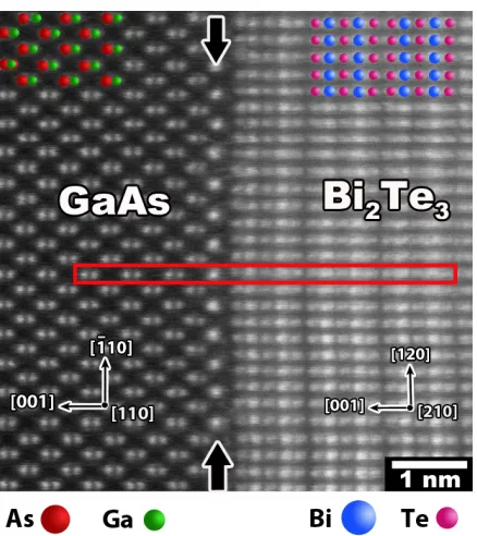
Figure 3.1 HAADF STEM image of the atomically abrupt Bi2Te3(right)/GaAs
(left) interface viewed down 110GaAs. The atom column identities
are denoted by the labels, and the terminal interfacial layer is in-dicated by the highlighted region. Figure reproduced from Ref. [2] with permission from AIP Publishing LLC (AIPP), Copyright 2013. 49 Figure 3.2 Intensity profile across the Bi2Te3/GaAs interface from the region
indicated by a red box in Figure 3.1. Figure reproduced from Ref. [2] with permission from AIP Publishing LLC (AIPP), Copyright 2013. . . 51 Figure 3.3 Atomic EDS map across the Bi2Te3/GaAs interface where the
dot-ted lines indicate the interfacial region. Both raw and noise filtered versions are shown for the constituent maps. The images show that Te dominates the signal at the interface with atomically resolved columns. Figure reproduced from Ref. [2] with permission from AIP
Publishing LLC (AIPP), Copyright 2013. . . 52
Figure 3.4 EDS line profile across the Bi2Te3/GaAs interface chemistry show-ing an atomically resolved Te X–ray signal. The EDS signals from Figure 3.3 were integrated parallel to the interface and averaged using a three-pixel box filter to reduce noise. Figure reproduced from Ref. [2] with permission from AIP Publishing LLC (AIPP), Copyright 2013. . . 53
Figure 3.5 Simulated and experiment images for the Bi2Te3/GaAs interface
Figure 3.6 Schematic of the Bi2Te3/GaAs interface structure showing the lo-cation of a quarter unit cell of Ga2Te3 at the interface. The vertical lines are provided to separate the distinct regions of the sample. The arrows indicate positions where Te is present between Bi2Te3 and Ga2Te3. Figure reproduced from Ref. [2] with permission from
AIP Publishing LLC (AIPP), Copyright 2013. . . 55
Figure 4.1 (a) Powder diffraction pattern and bright-field TEM image of a typ-ical Bi2Te3−xSex nanocomposite sample with (c) a corresponding
atomic resolution HAADF STEM image (probe convergence semi-angle 13.5 mrad) and schematic of the projected unit cell [bismuth (blue)/tellurium (red)]. Figure reproduced from Ref. [1] with
per-mission from Cambridge University Press, Copyright 2015. . . 59
Figure 4.2 (a) HAADF image of Bi2Te3−xSex aligned with atomic resolution
EDS maps revealing the preferential segregation of Se in the
struc-ture (probe convergence semi-angle 13.5 mrad). (b) Schematic Bi2Te3−xSex
alloy structure for each atom row and bond type. (c) Bond lengths in the quintuple layer structure measured using RevSTEM and XRD. 61 Figure 4.3 (a) HAADF image of Bi2Te3−xSex aligned with atomic resolution
EDS maps revealing the preferential segregation of Se in the
struc-ture (probe convergence semi-angle 13.5 mrad). (b) Schematic Bi2Te3−xSex
alloy structure for each atom row and bond type. (c) Bond lengths in the quintuple layer structure measured using RevSTEM and XRD. 63 Figure 4.4 Standard deviation of the distance between nthnear-neighbor atom
columns measured for h100i Si before and after correcting residual scan distortion. Figure reproduced from Ref. [1] with permission
from Cambridge University Press, Copyright 2015. . . 70
Figure 4.5 Plot of the spread in the calibration values obtained from silicon relative to the absolute Si lattice parameter. . . 70 Figure 4.6 (a) HAADF STEM image of pure Bi2Te3 alongh100iwith the
Figure 4.7 (a) HAADF image of Bi2Te3−xSex aligned with atomic resolution
EDS maps revealing the preferential segregation of Se in the
struc-ture (probe convergence semi-angle 13.5 mrad). (b) Schematic Bi2Te3−xSex
alloy structure for each atom row and bond type. (c) Bond lengths in the quintuple layer structure measured using RevSTEM and XRD. Figure reproduced from Ref. [1] with permission from Cam-bridge University Press, Copyright 2015. . . 79
Figure 5.1 Atomically resolved EDX signal from experiment for Ti-K, Sr-K,
and O-K as a function of convergence angle and thickness. Each map has been lattice averaged with a single unit cell template. The scale bar indicates 3.9 ˚A, the lattice parameter of STO. . . 85
Figure 5.2 Atomic resolution EDX signals collected from experiment and
sim-ulation. (a) Example of the experimental lattice averaged Ti signal acquired using a 14 mrad convergence semi-angle with an over-laid 2-D Gaussian fit. The red and blue planes indicate the back-ground and column signals. (b-c) Experimental and simulated col-umn, mean, and background signals from atomic resolution EDX maps for Ti-K (b) and Sr-K (c) for convergence semi-angles of 14 mrad and 20 mrad. (d-e) Contrast ratios for Ti-K (d) and Sr-K (e). (f) Ratio of the contrast for 14 mrad divided by the contrast for 20 mrad. Both plots are consistently above the dashed line reference at unity, indicating that the 14 mrad probe provides consistently greater contrast than the 20 mrad probe. Figure reproduced from Ref. [4] with permission from Elsevier, Copyright 2016. . . 86
Figure 5.3 Atomic resolution EDX signals collected from experiment and
Figure 5.4 Simulated atomically resolved EDX maps for varying thickness and convergence angles for (a) Ti-K and (b) Sr-K. The scale bar repre-sents 3.9 ˚A. Figure reproduced from Ref. [4] with permission from Elsevier, Copyright 2016. . . 91
Figure 5.5 Atomically resolved EDX atom column contrast (a-b) and the
num-ber of relevant ionization events caused as a fraction of the incident beam (c-d) as a function of convergence angle and thickness for Ti and Sr. Figure reproduced from Ref. [4] with permission from El-sevier, Copyright 2016. . . 93 Figure 5.6 Schematic of the orderedγ0-Ni3Al<001>structure with indicated
Ni-Ni (green) and Al-Al (red) atom column separations (a). Atom column contrast (b-c) and x-ray yield as a fraction of the electron beam (d-e) as a function of convergence angle and thickness for Ti and Sr. Figure reproduced from Ref. [4] with permission from Elsevier, Copyright 2016. . . 94
Figure 5.7 Effects of the amorphous surface area on the Ti (a) and Sr (b)
contrast for two convergence angles using a finite effective source size of 1.6 ˚A. . . 95 Figure 5.8 Effects of dwell time in atomically resolved EDX. (a) Total collected
X-ray counts collected per second in an EDX map for 14 mrad and 20 mrad convergence angles plotted as a function of dwell time. Counts are integrated from the entire 2-D map and energy range. (b) X-ray elemental maps collected with varying the dwell time us-ing a convergence angle of 14 mrad with intensities based on the counts in each individual map. Each map was taken at a sample thickness of 25 nm. The scale bar represents 3.9 ˚A. Figure
repro-duced from Ref. [4] with permission from Elsevier, Copyright 2016. 97
Figure 5.9 Simulated and experimental TiK/SrK ratios as a function of
thick-ness for 14 mrad and 20 mrad. . . 100
Figure 6.2 EDS HAADF and elemental maps for (a) the sample with a Ba interlayer and (b) the NO treated sample. Figure reproduced from Ref. [5] with permission from AIP Publishing LLC (AIPP), Copy-right 2016. . . 107 Figure 6.3 EDS spectra for different regions indicated from Figure 6.2. Figure
reproduced from Ref. [5] with permission from AIP Publishing LLC (AIPP), Copyright 2016. . . 108
Figure 6.4 HAADF RevSTEM images for the NO annealed (a) and Ba
inter-layer (b) samples. Strain maps represented by the overlaid boxes on the original RevSTEM images for the xx (c,d) and yy (e,f)
direc-tions with colors corresponding to the color bar on the right. Figure reproduced from Ref. [5] with permission from AIP Publishing LLC (AIPP), Copyright 2016. . . 109
Figure 6.5 HAADF STEM images acquired before (a) and after positioning
the beam at a point on the interface (b). (c) Line profiles across the interface from (a) and (b). Boxes with arrows overlaid represent the area used for the line profiles in (c). . . 111
Figure 7.1 Overview of the AlGaN films grown on sapphire and AlN native
substrates during the same growth run. . . 118
Figure 7.2 Higher magnification HAADF STEM images for each set of QWs
for both sapphire and AlN substrates. . . 119
Figure 7.3 EDS map from the characteristic Ga-K X–rays with a line profile
of the composition determined using the Cliff–Lorimer approach. . 121
Figure 7.4 RevSTEM strain mapping across a single QW for the sapphire and
AlN substrates. . . 122 Figure 7.5 Strain profiles indicating the average strain from each horizontal
row from the strain maps in Figure 7.4. . . 123
Figure 8.1 Images from the reconstructed oxide surface on c–plane AlN
ori-ented along the [11¯20] and [1¯100] directions. Illustrated atomic models for each direction are shown below the images with the clear presence of an inversion plane. Numbers 1,2,3 refer to the stacking position for the atoms. . . 128
Figure 8.2 ADF image and EELS map for the oxide surface reconstruction.
The spectrum corresponding to the horizontal position in the maps is shown on the plot to the right. . . 130 Figure 8.3 Measured distances at the reconstructed oxide surface with average
Figure 8.4 Illustration and experimentally observed image of steps on c–plane AlN surfaces. Colors of the circles corresponds to the horizontal stacking position. . . 135
Figure 8.5 ADF STEM image of the atomically clean m–face surface in AlN. 136
Chapter 1
Introduction
The development of materials is increasingly dependent on the ability to manipulate and
control structure and chemistry at the atomic dimensions. At such scales, properties are
often mediated by features such as interfaces [6, 7], point defects[8, 9], and free surfaces
[10, 11]. This is thus need for tools to characterize structure and chemistry at relevant
length scales. Structural characterization techniques based on diffraction, such as
X-ray diffraction (XRD) and neutron diffraction (ND) provide highly precise information
on the overall structure and chemical makeup, but information is globally averaged.
Interest in localized features such as interfaces emphasizes the need for another means of
characterization.
Often complementary to XRD or ND, transmission electron microscopy (TEM) has
the capability to probe information at the atomic scale, providing insight into local
fea-tures inaccessible by conventional diffraction methods. TEM and scanning transmission
electron microscopy (STEM) have been widely used to probe spatially confined
infor-mation, but the development of aberration correction has created a paradigm shift in
sin-gle atoms [12, 13, 14, 15, 16]. More recently, methods have been introduced to place
STEM image intensities on the same scale as simulation [17], enabling studies to
mea-sure composition [18], thickness [19], and determine the number of atoms within a column
[20, 21, 22].
Figure 1.1: Typical HAADF STEM images of [110]GaAs acquired on an uncorrected
JEOL 2010F (blue box) and probe-Cs corrected FEI Titan (orange box). Integrated
intensity profiles from each image are shown on the plot to the right which represents the intensity across the horizontal direction indicated by the arrows. The black bar represents 1 nm.z
Figure 1.1 shows examples of typical images of [110] GaAs acquired with a microscope
with and without an aberration corrector. Acquisition using the aberration–corrected
microscope provides clear separation of the Ga–As dumbbells. From more than a visual
improvement, the probe-corrected image shows that the left column in each dumbbell is
dimmer than the right. Based on the known structure, GaAs, the polarity of the structure
can be identified knowing that the image is sensitive to the atomic number. For this case,
Ga, Z = 31, comprises the left position of the dumbbell and As, Z = 33, resides in the
right column. For the uncorrected image, it is not possible to discern the polarity of the
structure.
STEM, there are many cases that restrict access to compositional information in which
using ADF STEM alone is ambiguous at best[23, 24, 2, 25]. One such example is shown
in Figure 1.2 where a bright column of atoms is observed between GaAs and Bi2Te3. By
extracting the intensity across the red box, the intensity of the bright column corresponds
most closely to the Bi intensity in Bi2Te3. By a simple Z2 interpretation of the image
intensity, one would expect the bright column to be comprised of bismuth. It is shown
later in this work that this is not the case and other methods must be employed to resolve
the elemental makeup.
1.1
Spectroscopy inside the transmission electron
mi-croscope
Because ambiguities can occur using HAADF alone, obtaining information that is
char-acteristic to the atom type, i.e. spectroscopy, is invaluable. Using STEM it is now possible
to collect spectroscopy and ADF signal simultaneously [26, 27]. One spectroscopic
tech-nique in the TEM is energy–dispersive X–ray spectroscopy (EDS) which relies on the
ionization of bound electrons in the sample excited from the primary electron beam. In
the past, EDS was very limited for characterization in the TEM due low signal. The
X–ray emission occurs spherically, resulting in an emission solid–angle of 4π sterradians.
The collection solid-angle of a single detector however is only approximately 0.2
sterra-dians, resulting in a majority of the electrons not being collected. Conventionally, EDS
inside the TEM was restricted to nanoscale analysis [28, 29, 30, 31]. Recent innovations
in detector technology have greatly improved the collection solid angle, resulting in the
ability to map chemistry at the atomic scale [32, 33, 34, 35].
Figure 1.3 shows the signal obtained from HAADF and EDS for a Bi2Te2.7Se0.3 alloy. Without EDS, it was not known where Se resides in the structure, but by performing
EDS, Se is shown to reside in the center column.
1.2
Motivation and organization
Complete structural characterization requires an understanding of the atoms present in
a position and the distance between neighboring atoms. Although many methods enable
determination of local chemistry, accurate methods for determining distances have
re-mained elusive. Methods have resulted in highly precise measurement [36, 37]; however,
highly precise methods require a reference structure within the sample image to
pro-vide absolute structure measurements. In many cases, areas of known structure are not
available in the same image such as strained samples or materials of unknown chemistry.
Although many benefits exist using STEM, many limitations in STEM imaging
re-main. Because scan coils are responsible for rastering the electron beam across the sample,
any imperfections in the scan strengths or directions will induce distortions to the STEM
image [1, 38, 39]. Further, even for a perfect scanning system, other distortions will occur.
Because of the nature of scanning, each pixel is collected at a different time than the each
of the other pixels. It is important to note that while the sample is in the microscope,
there is always a change in the sample position as a function of time, which is what we
refer to as drift. As the sample drifts during scanning of the electron beam, the actual
distance and angle between pixels will be dependent on the drift rate and direction.
For EDS, although spectrum mapping can provide elemental information, several
major limitations on the quantifiability remain. In comparison to ADF imaging the signal
Several approaches have been employed to overcome low signal–to–noise ratios such as
increased beam current, increased collection time, or template averaging which creates
image based on the average of several areas [40, 41, 42]. For the cases of increasing beam
current and collection time, the sample is exposed to a larger beam dose often creating
damage of the sample. Of the mentioned approaches, template averaging been proven
useful for several studies such as fast EDS mapping to monitor phase transformations
[43, 44]. However, with this approach, local atomic scale information is averaged, resulting
in a loss of detail on an atom–column by atom–column basis. Methods for improving the
signal to noise for quantifying local composition are needed.
1.2.1
Technique Development
In this thesis, methods for improving the quantitative capabilities in STEM are
devel-oped. First, a calibration routine for enabling accurate distance measurements is
de-veloped, providing bond length information on an atom column–by–column basis. By
employing Revolving STEM, a method to minimize sample drift, and implementing a
newly developed calibration routine for restoring distorted images to their true state,
im-ages with highly accurate distance and angle values are produced. The technique is then
applied to the Bi2Te3 – Bi2Se3 alloy system and shown to determine lattice parameters
with lower than 0.1 % error relative to synchrotron XRD [1]. The technique is further
employed to accurately quantify strain in various systems providing insight into a variety
of structure–property relationships [45, 46, 47, 48].
Further, methods for improving the signal–to–noise ratio in EDS are developed to
improve the visibility of atom columns in EDS mapping. By changing the convergence
of the atom column signal above the background by appropriately selecting the
appropri-ate convergence angle. Next, the effects of sample thickness on the atom column contrast
and signal are shown. Finally, the effects of dwell time during mapping are shown which
have a significant effect on the processed counts in the spectrum maps.
1.2.2
Applying developed methods to solve materials problems
Chapter 3 provides a study showcasing the power of combining HAADF STEM imaging
with STEM EDS to unambiguously resolve the Bi2Te3–GaAs interface. Bismuth telluride
and its alloys are common thermoelectric materials employed in power generation and
refrigeration [49, 50, 51]. Bi2Te3 thin films exhibit profoundly increased thermoelectric
performance. As film thickness decreases, the properties become dominated by surface
and interface characteristics. Integration of Bi2Te3 thin-film functionality with electronic
devices requires growth on a range semiconducting substrates. Bismuth telluride has
a rhombohedral crystal structure and belongs to the R¯3m space group. Typically, high
quality exitaxial growth requires substrates with a similar structure symmetry and lattice
spacing. However, the growth of Bi2Te3 (001) on GaAs (001) has exhibited high quality
epitaxy even though there is a drastic symmetry change between the 4-fold (001) GaAs
and the 6-fold (001)Bi2Te3surfaces. Direct atomic structure imaging reveals an atomically
abrupt interface with a bright layer of atoms which would typically indicate atoms with a
higher atomic number. Upon investigation with EDS and multislice simulations however,
the bright column is shown to be comprised of a higher density of lighter elements,
Te. These results highlight the need for combining information from ADF imaging and
spectroscopy to provide an unambiguous interpretation of the interfacial structure.
interfaces. Silicon carbide has become a prominent wide-bandgap material for metal
ox-ide semiconductor (MOS) devices, particularly in power applications [52, 53, 54, 55].
Al-though SiC devices exhibit great properties at high power and high temperature, interface
trap density at the SiC/SiO2 interface limits the field-effect mobility (µF E) [56, 57, 58].
By depositing a Ba interlayer, resulted in a highly improved field–effect mobility [59, 60].
By resolving the interface, The Ba interlayer treatment displays a diffuse bright
interfa-cial layer while the NO treated sample appears to be atomically abrupt between the SiC
and SiO2 layers. Using energy dispersive X-ray spectroscopy (EDS), the interfacial layer
in the Ba treated sample is shown to contain Ba. Further, N is shown to appear at the
NO annealed interface. To understand how the different interfacial treatments affect the
local structure, accurate crystallographic measurements are employed to determine the
strain state for samples that undergo different treatments. For Ba treated samples, there
is no observable strain at the interface, while compression is shown for the NO treated
sample which can affect the gate field–effect mobility.
In Chapter 7, the developed method for accurate real space crystallographic
mea-surements is employed to Al1−xGaxN heterostructures to determine structural behavior
at interfaces. AlN based materials are commonly employed for blue and deep
ultravi-olet (UV) LEDs with emission wavelengths dependent on the composition. One major
issue with modern Al1−xGaxN devices is compositional pulling, which is the formation
of a transition layer consisting in an intermediate composition. Using accurate
crystal-lographic measurements, we image two different samples grown with the same growth
conditions but on different substrates, sapphire and AlN. For the sapphire sample, we
observe compositional pulling, but for the AlN sample we observe no pulling effects. In
contrast to conventional strain mediated mechanism, we present an alternative
interface for QWs with varying composition grown on different substrates. For samples
grown on sapphire substrates, compositional pulling is observed, but no pulling is
ob-served when grown on AlN under the same growth condtions. Further, we show that
even for samples grown at the same time in the same reactor, growth layers will be
com-prised of different compositions for different substrates. Although the compositions are
different, we show that QWs with higher Ga composition grown on AlN do not exhibit
compositional pulling. We further show that the strain conditions for different are similar
for QWs on AlN and sapphire substrates and that the pulling effect is mediated by the
surface morphology rather than strain driven.
In Chapter 8, accurate distance mapping is applied to resolve atomic surface
recon-structions and changes in bond distance in comparison to the bulk structure. In
particu-lar, the formation of an inversion boundary on the surface of c–plane AlN and GaN. By
combining RevSTEM imaging and EELS we directly determine the local chemical and
bonding environment. Further, we will show that first principles DFT simulations result
in lower surface energies than previously proposed models.
Finally, conclusions will be made on the consequences of this work and the
Chapter 2
Background and Methods
This section examines the steps of TEM sample preparation, experimental operating
conditions, and data analysis techniques used throughout the thesis. In several cases,
there will be slight variants to the procedures described here that are tailored to the
materials and analysis required in the following chapters, but these methods will serve
as a guideline for the work performed throughout the dissertation.
2.1
Sample Preparation
The most important step for obtaining meaningful TEM data is the preparation of high
quality samples. Even the most skilled operator using the most powerful microscope
in the world cannot overcome a poorly prepared sample. To meet the criteria for high
quality samples, several standards must be met: (1) The structure at the area of interest
must not be altered during preparation. (2) The sample must be at least as thin as the
intent of the experiment requires. (3) The sample should contain minimal contaminant or
including focused ion beam (FIB), electropolishing, dispersion, exfoliation, or mechanical
polishing. For the purpose of this work, the most heavily relied upon method is mechanical
polishing. In this section, I will present an overview of mechanical wedge polishing as well
as many of the variations employed to achieve prepare more difficult samples.
For mechanical polishing, the starting material is commonly a bulk crystal that is
either single crystalline or polycrystalline. In either case, the initial step is to section the
bulk crystal into smaller rectangular pieces. The bulk crystal is adhered to a glass slide
using Crystalbond. If the sample has a thin film, the film side is placed in the Crystalbond
to reduce damage during cutting. An Allied Techcut 4 low speed saw equipped with a
diamond coated blade was used to create precise cuts with minimal cutting width which
results in a lower amount of the crystal to be lost during cutting. Samples are then cleaned
using acetone and isopropanol. Either M-bond or Epoxybond 110 is applied to the film
side of one sectioned piece and another is placed on top, resulting in a sandwich with films
facing one another. The sandwiches are then cured so good adhesion is assured. Once
the sandwich has cured, it is placed with the glue line perpendicular to the pyrex surface
of a TEM paddle using Crystalbond to adhere the sample to the paddle. The sample is
then polished to the to the finest available film size, then flipped so the polished surface
is facing the pyrex stub and polished again until the sample is approximately 30 µm. At
this point, the front micrometer of the Multiprep is descended so that a 2◦ angle between
the pyrex stub face and the polishing wheel is created. The sample is further polished
until the sample is as thin as can be managed. Figure 2.1 shows the steps involved in
conventional wedge polishing. A Mo TEM grid is then placed on the stub using M-bond
for adhesion.
For further thinning, the TEM sample is commonly ion-milled using a Fischione 1040
effectiveness. A few of which are shown schematically in Figure 2.2. The conventional and
most commonly used method through this work is shown in Figure 2.2 (A). The guns
are fired perpendicular to the glue line which has anecdotaly been shown to cause less
damage for thin films than the approach in Figure 2.2 (B). Further, for bulk samples, this
will result in a larger thin area along the front edge. One ion milled induced artifact is
the introduction of Mo and Ti signal when performed spectroscopy which occurs because
of sputtering of the TEM grid and ion mill posts during the milling process. To produce
larger thin sample areas, lower ion milling angles are typically used. Because the ion beam
has a finite size, a portion of the beam encounter the TEM grid and sputter the TEM grid
material. As an attempt to reduce the sputtering, the portion of the TEM grid thought
to sputter has been removed, successfully milled, and imaged at atomic resolution. The
approach in fact resulted in much less Mo signal; however, the forces to remove a section
of the grid introduced a large amount of bending, creating new problems for TEM. The
prospects of the approach remain promising, as there are numerous better approaches
for machining similar grids without the induced bending.
For many materials conventional preparation is insufficient for obtaining high quality
samples. The preparation of high quality AlN TEM samples is notoriously difficult due
to the brittle and physically hard properties. For wedge polishing of brittle materials, the
thin area near the wedge tip can readily crack or cleave, leaving the remaining sample
relatively thick. For example, a previous wedge polishing study reported that the
prepa-ration of thin films of GaN on a sapphire substrate requires very careful monitoring that
results in a long time commitment at the final thinning steps [61]. To avoid cracking and
cleaving, fil ms with fine particle sizes, slow rotational polishing speeds and low pressures
must be used. For hard materials, this results in an unreasonably long polishing time to
Figure 2.1: Overview of the steps involving in conventional wedge polishing. (a) bulk crystal is adhered to a glass slide and diced along the dotted lines. (b) Diced sections are glued together. (c) Resulting sample stack. (d) Sample is adhered to pyrex stub. (e) Sample is polished. (f) The pyrex stub is tilted so that the sample is inclined relative to the polishing platen.
2.2
Preparation of samples with brittle substrates
Mechanical polishing provides a route towards preparing thin samples [62]. Wedge
polish-ing has become a widely used technique to produce areas below 5 nm thick [15]. For many
brittle and hard materials, inevitable cracking and cleaving occurs in the substrate during
wedge polishing, shown in Fig. 2.3. A previous study using wedge polishing was reported
for preparing thin samples of GaN on a sapphire substrate although the process requires
very careful monitoring, resulting in a long time commitment at the final thinning steps
[61]. For physically hard materials, cracking and cleaving proves problematic for wedge
polishing because the thin area near the wedge edge will detach from the sample leaving
the useable sample area relatively thick. To avoid cracking and cleaving, films with fine
particle sizes, slow rotational polishing speeds and low pressures must be used. For hard
in many cases cracking will continue to occur. For many devices, an AlN substrate is
required for high quality film growth. However, the AlN has a higher hardness and lower
fracture toughness than sapphire, resulting in more cracking and a longer polishing time.
To the best of our knowledge, a method for preparing high quality AlN has not been
reported.
Figure 2.3: Schematic of a cross-sectional thin film sample before (left) and after (right) mechanical wedge polishing. Cracks are shown to propagate from the thin area in the substrate throughout the sample. Cleaved areas are shown below the bottom edge.
In order to achieve extremely thin conditions, low energy ion milling is often
em-ployed. In order to study the atomic structure, the sample structure must be preserved
during sample preparation. However, many consequences can occur during the milling
process such as amorphitization [63, 64], preferential milling of different sample layers
and redeposition of sputtered material on the sample which convolutes interpretation of
be damaged will mill at a faster rate than the substrate and interpretation of the sample
becomes obscured. An alternative method for sample preparation is desired to improve
sample quality while reducing the amount of polishing and ion milling time to prepare
TEM samples.
In this study, we present a method to trivialize the difficulties encountered from
preparing sample with hard and brittle substrates. Samples with AlN and sapphire
sub-strates have been prepared in a period of several hours, reducing the polishing time
by more than a factor of four. In contrast to conventional preparation, this method
re-quires minimal ion milling energies and time to achieve extremely thin conditions. Using
STEM, we show atomic scale images clearly revealing the atomic structure with regularly
observed areas as thin as 10 nm.
2.2.1
Sample preparation procedure
Bulk AlN and sapphire with an alternating AlGaN/AlN thin film were used for TEM
sample preparation. Bulk samples were sectioned into 1 mm x 1 mm sections using an
Allied diamond saw. Two sections from the same bulk material were then mounted on a
TEM lapping paddle using crystalbond with the thin film, if applicable, faced into the
wax, shown schematically in Fig. 2.4 (a). Samples were then polished to approximately
50 µm using diamond lapping films of 30 µm and 9 µm. To reduce cost, 30 µm and 9
µm SiC lapping films were used rather than diamond for polishing of AlN. Sections of
silicon with the same dimensions were then adhered to the substrate to form Si-stacks,
Fig. 2.4 (b), using M-bond 610 and heated at 160 ◦C for two hours to cure. Sections of
the bulk material attached to Si were placed in a dish of acetone followed by isopropanol
surfaces.
From this point, samples were prepared in a conventional cross-sectional wedge
pol-ishing approach. M-bond 610 was dropped onto the film side of one Si-stack. The other
Si-stack was then placed to face the film with M-bond. The cross-sectional sample was
then held at 160◦ C for two hours to cure. The sample was then remounted on the TEM
lapping paddle to polish material in cross-section, shown schematically in Fig. 2.4 (c),
and polished until a uniform surface finish was achieved using 9µm, 3µm, 1µm, and 0.1
µm diamond lapping films. The sample was then flipped 180◦so that the polished surface
is placed in crystalbond. The sample was polished to an approximate thickness of of 100
µm then 30 µm using 9 µm and 3 µm diamond lapping films respectively. The sample
was then wedged with a 3.5◦ angle with 1 µm and 0.1 µm lapping films until thickness
fringes were observed in silicon for the Si-stack samples. Conventionally polished samples
were polished until no increase in fringes appearance was observed. For further thinning,
low energy ion milling was used. All samples were ion milled at LN2 temperature with
energies of 0.8 keV and 0.5 keV for five minutes and ten minutes respectively. Samples
were ion milled at the same conditions to compare the differences in mechanical polishing.
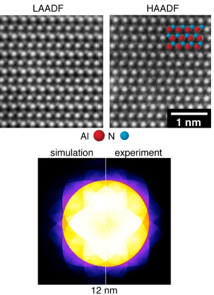
Low-angle annular dark-field (LAADF) and high-angle annular dark-field (HAADF)
imaging was performed using a probe corrected FEI G2 Titan 60-300 kV STEM operated
at 200 kV with a 20 mrad probe forming convergence semi-angle. The probe current was
50 pA. To improve the signal to noise ratio and better evaluate how well the atomic
structure was preserved, a series of 20 frames were acquired and averaged using revolving
STEM (RevSTEM) [65]. For thickness determination, position averaged convergent beam
electron diffraction (PACBED) was employed and matched with simulated PACBED
2.2.2
TEM sample quality
Fig. 2.5 (a) shows the conventional polishing method before the beginning of wedge
pol-ishing. Even at thicknesses of approximately 30µm, cleaving parallel to the sample edge
occurs, as indicated by the arrows. During wedge polishing, the edge of the sample will
recede as the front edge is continually polished away. To produce samples with a smooth
interface, the sample must be polished until all of the cleaving is removed otherwise the
sample will break off at the cleavage site. The Si-stacking method we describe shows the
sample shown after the same polishing step, Fig. 2.5 (b). The amount of cleavage is
re-duced but not completely eliminated. However, the substrates are now bound strongly to
the Si by M-bond and even if cleavage is present behind the thin area during wedge
polish-ing, the sample will stay intact. Once the samples are wedge polished, large cracks often
form and propagate to the interface for conventionally prepared samples. By minimizing
the substrate thickness, the sites which cracks can propagate from is also minimized.
Further, for conventional polishing, an extensive amount of time required to polish the
front edge and reduce cracking and cleaving during conventional polishing and is by far
the most time consuming step. By reducing the substrate area from 500 µm to 50 µm,
the area of the substrate that is polished is reduced by a factor of ten and proportionally
reduces the polishing time.
By using the same polishing force over a much smaller area however, the pressure
on the area would greatly increase and result in more cracking. By adhering Si on both
polished substrates, the force is again distributed over a larger area. Si polishes much
more quickly than substrates of Al2O3 and AlN, resulting in a cross-sectional sample
that polishes faster and with many fewer sites for crack propagation and cleaving than a
µm thick becomes unwieldy so the extra Si layers allow for more precise manipulation.
Samples were wedge polished until thickness fringes stopped becoming more
pro-nounced in the conventionally polished approach, Fig. 2.5 (c), and until silicon thickness
fringes were observed in the Si-stacking method, Fig. 2.5 (d). Although thickness fringes
occur for both samples, the fringes appear more pronounced for the Si-stacking method
even efforts to continue to polish to thinner conditions for the conventional method were
made. During conventional wedge polishing, fragments of AlN would cleave from the thin
edge, reducing the amount of thin area. Cleaving also occurred for the Si-stack method,
however, it appears that more thin area was able to stay intact. It should be noted that
because the samples were bulk crystals without a thin film, the cross-section interface is
fairly large due to the roughness. Also, for Fig. 2.5 (d), the varying contrast beneath the
sample is due to water.
After the samples were mechanically thinned, they were both ion milled at low
en-ergies, 0.8 keV and 0.5 keV, for five and ten minutes at each respective energy. The
sample following ion milling are shown in Fig. 2.5 (e,f). Both samples exhibit more
in-tense thickness fringes than the previous step, but the fringes for the Si-stacking appear
more strongly, indicating that the conventionally polished sample requires additional ion
milling to reach similar thin conditions.
Table 2.1: Time and cost reported for bulk AlN using Si stacking and conventional mechanical wedge polishing methods.
Method Polishing time (hr) Curing time (hr) Diamond films (#) Total cost (USD) Si-stack 1.50 4.00 3 78
Conventional 6.25 2.00 5 130
2.1. The polishing time required was shorter for the Si assisted method than for the
conventional method. Even though the curing time is two hours longer for the Si assisted
method, the overall time remains shorter and the operator may pursue other projects
while the sample cures. Additionally, the number of lapping films used to polish the
sample was greater for conventional polishing than for the Si-stack method. Furthermore,
the greater polishing time and ion milling time will increase the cost even more if the
preparation facility charges an operation fee.
Although the samples were prepared more quickly, it is essential that the samples are
of high quality. To answer questions about the sample quality for the Si-stack method,
high-angle annular dark-field (HAADF) and low-angle annular dark-field (LAADF) STEM
were employed, shown in Fig. 2.6(a) and (c). The LAADF signal is more sensitive to
diffraction contrast while HAADF is sensitive to mass-thickness contrast. For each image,
the atomic columns are clearly resolved. The crystalline thickness is reported by
match-ing the experimental position averaged convergent beam electron diffraction (PACBED)
with simulation shown in Fig. 2.6 (c). Similar sample areas were observed throughout
the edges of the sample and sample areas as low as 4 nm were observed.
From more than a sample quality and time reduction standpoint, the approach
of-fers the traditional advantages of silicon polishing. During flat polishing, the silicon will
change color from red to yellow at thinner conditions [66, 67]. Further, simply using
thickness fringes of a substrate for substrates such as Al2O3 and AlN does not
necessar-ily guarantee that the sample is thin. However, due to silicon’s higher refractive index,
thickness fringes only appear once the sample is much thinner, (<2 µm), in comparison
to when Al2O3 and AlN fringes appear. For studies that require a structure of known
area to calibrate image distances and distortions, the silicon layer can be used without
preparation and imaging of a separate sample.
2.3
Wedge polishing of 2-D layered materials
Conventional wedge polishing provides a simple and reliable method for preparing films
grown on managably thick substrates, i.e. thicknesses>100µm. For the case of 2D layered
materials, the extremely thin conditions are problematic for wedge polishing. Typically,
Figure 2.7: Schematic of a cross-sectional thin film sample before (left) and after (right) mechanical wedge polishing. Cracks are shown to propagate from the thin area in the substrate throughout the sample. Cleaved areas are shown below the bottom edge.
in cross–section is preferable. To prepare cross section samples, we first exfoliate thin
layers from a bulk sample followed by adhering the layers on two different 2 mm ×2 mm
single crystal of silicon. Samples are then glued together using M-bond 610 in a similar
fashion to conventional wedge polishing. An illustration of the procedure is presented in
Figure 2.7. This method was performed to obtain TEM samples for the pure Bi2Te3 and
Bi2Se3 compounds in Chapter 4.
2.4
Atomic scale imaging in the transmission
elec-tron microscope
There are major methods for atomic structure analysis in the TEM: high resolution TEM
(HRTEM) and scanning transmission electron microscopy (STEM). Although both
tech-niques provide atomic scale information, the electron optics are different. For HRTEM,
a parallel electron beam passes through the thin specimen. After the beam – sample
to form a coherent interference pattern. At the atomic scale, the scattering potential
from each atom in the specimen leads to a phase shift resulting in interference dependent
on the atomic structure. At the atomic scale, the interference pattern is sensitive to
pa-rameters such as defocus and crystal thickness. Interpretation of the location of atomic
positions becomes complex and if quantification of atomic positions is desired, a series of
simulations with varying thickness and defocus are essential. Such factors make analysis
of unknown samples rather complicated.
For STEM imaging, an ˚A sized convergent electron probe is formed and scanned
across the sample on a pixel–by–pixel basis, where scattering occurs through the
sam-ple. Perhaps the most commonly used STEM technique is high–angle annular dark–field
(HAADF) imaging which the detector positioned to collect highly scattered electrons,
forming an incoherent image. The incoherent imaging produces intensities that scale the
the atomic number and density of atoms within an atom column, unlike phase contrast
imaging [68, 69]. Consequentially, HAADF STEM images do not suffer from contrast
reversal and the positions of atom columns are directly interpretable, providing an
op-portunity for directly observing crystallography in real space.
2.4.1
Signals in the scanning transmission electron microscope
As scanning transmission electron microscopy is the primary instrument for this research,
a brief overview of the components and electron optics will be introduced. Starting at
the source of the electron beam, a Schottky field–emission electron source with high
brightness and coherent electron beam is used to generate the electron beam that travels
through the column. Once electrons are emitted from the source, the beam is focused
The electron is then focused using the objective lens. Figure 2.8 presents a diagram of
STEM at and below the objective lens. The convergence of the electron beam is often
characterized by the probe–forming semi–convergence angle, α, which is determined by
the cross–over point between the C2 and C3 condenser lenses. The converged beam is
then rastered across the sample by scan coils to image the specimen at a point–by–point
basis. The achievable spatial resolution is dependent on the quality of the electron gun
as well magnetic lenses. FEG sources are used for atomic resolution imaging rather than
thermionic emitters because the emission source is much smaller providing a more
coher-ent source. Further, any imperfections in the lenses will induce aberrations that distort
the probe and degrade image quality. Inevitably, aberrations will occur in electron
micro-scopes that consist of different symmetries and magnitudes. Two types of aberrations that
are most important to consider and difficult to correct are spherical (Cs) and chromatic
(Cc). Chromatic aberration is caused by spread in energy of the emitted electrons that
will result in unequal focusing of electrons. Spherical aberration arrises from a difference
in magnetic field strength applied to electrons traveling at different angles. Aberrations
create a spread in the ability to finely focus the probe known as the disc of least
con-fusion [70, 71]. Because of aberrations, apertures are used to cut off the contribution
from high angular ranges which are more heavily plagued by aberrations. Although the
aperture decreases the contribution of aberrations in the optics, using a smaller
aper-ture will decrease the convergence angle, which reduces the achievable spatial resolution.
The introduction of aberration correctors have allowed for users to increase the aperture
size and improve the capable spatial resolution as well as increasing the probe current
[72, 73, 74]. Most modern aberration correctors are set up to correct for Cs, leaving Ccas
the resolution limiting aberration. Because of the revolution of the aberration corrector,
Once the beam interacts with the sample, it scatters to various angles and generates
X–rays that can be collected by the EDS detectors. The most commonly used signal for
imaging comes from electrons scattered onto the ADF detector. Because of the flexibility
to change the effective detector positions, camera length, the angular range of scattered
electrons can be controlled to generate images based on electrons scattered at different
angles. By collecting electrons scattered to high angles, incoherent imaging is formed.
By collecting over a smaller angular range, more coherent imaging is formed, resulting
in images containing phase information. Further, it is possible to collect coherent and
incoherent images simultaneously by inserting a BF detector below the sample to collect
low scattered electrons while the ADF detector collects high angle scattering. In contrast
to conventional TEM, HAADF STEM imaging is easily interpretable with intensities
based on the sample structure, atomic number, that is preserved much better for different
thicknesses and defocus values. Additionally, an EELS detector can be placed below
the sample to disperse electrons based on their energies, providing spectra sensitive to
different scattering mechanisms such as plasmons, and inellastic collisions [75].
2.4.2
Scattering in the electron microscope
When the electron beam reaches the sample, the electrons from the beam can either be
transmitted or scattered. The electron microscope is set up to collect information from
the various processes. Electrons that are interact with the sample can be deflected by
various angles depending on the type of interaction. Electrons that are deflected without
any energy losses are known as elastic collions while those that result in energy loss
are inelastic collisions. Elastic scattering contributes most strongly to the signal in ADF
Electrons that undergo inelastic collisions will contribute to the collection of spectroscopic
signal by generating characteristic and Bremsstralung X–rays contributing to the EDS
signal as well as electrons with energy losses that will contribute to the EELS signal.
2.4.3
Multislice Simulations
Frozen phonon multislice calculations are often used to compare experimentally obtained
images with simulated structures by calculating the propagation of the wave function
through a thin sample. For multislice simulations, the sample is sliced into many sections
determined by periodically occuring units through depth [76]. The method can be used
to calculate image intensities at different locations on the sample as well as convergent
beam electron diffraction patterns and the distribution of the probe as it travels through
the crystal. Each slice of the sample represents the phase grating that in which the wave
function is diffracted. Afterwards, the resulting wave function travels by using a Fresnel
propagator to the following slice and the process is repeated. The final wave function
after exiting the crystal is used to produce the simulated image.
For more realistic simulations, several iterations of the multislice calculation must
be repeated to account for the vibrations that occur in real crystals. The time between
individual electrons that pass through the microscope column is much greater than the
lifetime of a phonon, meaning that each individual electron will encounter a crystal with
atoms in a different thermal displacement. Therefore, instead of simulations with atoms
residing at their exact lattice position, multiple simulations with varying phonon effects
must be simulated. The Debye–Waller factor quantifies the thermal vibration of atoms
within a crystal along different crystallographic directions. After simulations of different
2.4.4
Position Averaged Convergent Beam Electron Diffraction
In many cases, accurate determination of sample thickness is required to obtain
mean-ingful quantitative information from STEM images. Commonly, the log ratio method
method is used to determine sample thickness from EELS [77, 75]. However, the method
becomes increasingly inaccurate as the sample thickness decreases. Position averaged
con-vergent beam electron diffraction (PACBED) on the other hand, is created by scanning
the focused electron beam across the sample and averaging the CBED pattern from the
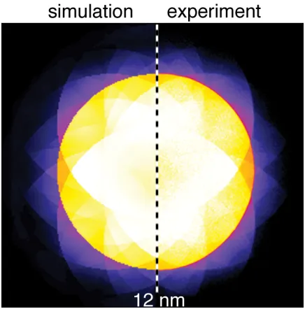
scanned area [78]. Figure 2.9 shows a simulated and experimentally collected PACBED
pattern acquired from a 12 nm thick AlN sample oriented along the [11¯20] direction. In
comparison to EELS log ratio thickness methods, PACBED is much more sensitive for
thin samples.
2.4.5
Revolving STEM
The ability for STEM to probe individual positions on a pixel–by–pixel basis serves as a
major strength but also a major limitation. Because the beam is rastered across an area
of the sample, each pixel is acquired at a different time. In an ideal case, there would
be no sample movement during image acquisition; however, inevitably, some movement
occurs during the imaging process. The resulting image is a distortion of the scanned
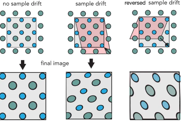
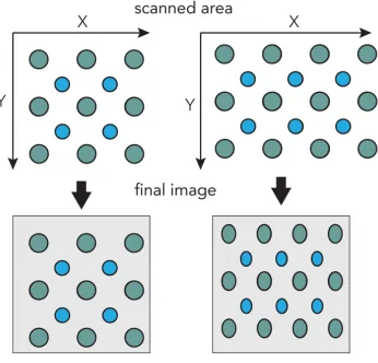
sample area represented by the square image. Figure 2.10 shows three cases: one with no
sample drift, the second with drift in towards the top right direction and the other with
drift towards the bottom right direction. For the ideal case, no distortion is observed for
the final image. For the scenario with sample drift, the red box representing the scanned
sample area is sheared into the proportions of the gray box which can be described by an
affine transformation. The resulting image shows large deviation in the lattice vectors,
originally perpendicular and has also scanned over a larger range. This means that the
scale of the resulting image is not only inaccurate in angle but also in distance with
respect to the ideal case. It is also important to note that the scanned sample area is
effected by the drift rate and direction. If we consider the previous case and increase the
magnitude of the drift rate, we will increase the range of the scanned sample area while
the distortion in the angles remains constant.
In STEM it is also important to consider the flexibility of the scan system. While
the previous image can be thought of as scanning from left to right with an immediate
flyback to the proceeding row, similar to english style of reading, the coils can scan in
any direction. If we instead scan starting from the bottom right of the box from right to
left and then flyback to the above row on the righthand side, the bottom rows will be
Figure 2.10: Schematic illustrating the effects of sample drift on STEM images.
images.
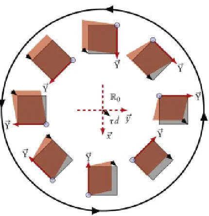
By removing the effects of drift, Sang and LeBeau [65], have created a technique
to minimize the deleterious distortions, Revolving STEM (RevSTEM). As illustrated in
Figure 2.11, the scan directions are changed which also affects the influence of drift. By
collecting many frames from the same area of the sample, it is possible to encode all of
the necessary information to correct for drift and restore the images to their ideal state.
Importantly, this is done without prior knowledge of the sample crystallography.
Although drift is minimized in the RevSTEM images, residual distortion remains in
the images due to imperfections in the scan coils. This occurs because of inequal strengths
of the the different scan coils, creating a dilation or skewing of the recorded image. Figure
2.12 shows an illustration of a distorted STEM image caused by unequal strengths in the
for scan distortion using a simple affine transformation. More details on the calibration
scheme and method are discussed in Chapter 4.
Figure 2.12: Illustration of the effects of scan distortion on the collected STEM images.
2.5
Data analysis
Once RevSTEM images are collected, information pertaining to distance and intensity
measurements becomes easily accessible. Of particular importance is the assignment of
atom columns to a uniquely indexed matrix representation. The first step towards this is
determining which crystallographic directions are of interest for the study. The
distribution of different lattice planes. Figure 2.13 shows an example of the PSD from a
GaN RevSTEM image oriented along the [11¯20] zone–axis. The major crystallographic
directions are shown to occur at 25, 90, 155, and 180 degrees. For the purpose of
measur-ing lattice parameters, we will consider the two direct