Multiplier Design Using Carry Save Adder
Avinash M. Ghorpade1, Amey Mahadeo Muchandi2
Associate Professor, Dept. of ECE, Maratha Mandal Engineering College, Belgaum, Karnataka, India1
PG Student [DECS], Dept. of ECE, Maratha Mandal Engineering College, Belgaum, Karnataka, India2
ABSTRACT:In this paper, we present a low power 32-bit multiplier design, by using Carry Save Adder (CSA). The multiplier design shown in this paper is modelled using Verilog language for 32-bit unsigned data. Optimizing speed and power constraints have become challenging tasks in the design of any reliable and efficient integrated circuit. This paper sets up the design of a 32-bit multiplier which is of high speed, and has low power consumption. By reducing the generated partial products the speed of the multiplier can be increased. There are many ways by which we can reduce the number of partial products generated in a multiplication process. Wallace tree multiplier method is one of them. Therefore, minimizing the number of half adders used in a multiplier will reduce the circuit complexity.
KEYWORDS: Carry Save Adder (CSA), Wallace Tree.
I.INTRODUCTION
Multipliers constitute a very important part of modern computing systems. Multipliers are mainly used in many electronic applications like Digital Signal Processing (DSP), where in multipliers perform various algorithms like FIR, IIR etc. DSP calculations usually involve use of multiply and accumulate operations. In computational systems the most important operation is multiplication. For any VLSI designer reducing the chip area and power consumption is a major challenge. The multiplier performance plays a crucial role in the field of Graphics and Process control. Depending upon the output requirements of the application the multiplier structure will vary drastically. Selection of optimum design structure is the very first step of the design process. Multiplication operation can be performed using various structures starting from serial multipliers and ranging up to complex parallel multipliers. Speed improvement of any sought whatsoever in the multiplier will increase or intensify the frequency of the DSP or can be exchanged for energy by optimizing the circuit size and the voltage supply. Some of the important considerations in the fabrication of DSP systems and high performance systems are smaller area and low power consumption. A major design issue is reducing the chip area and increasing the speed of the multiplier. However, area and speed are usually inversely proportional to each other i.e. improving speed of the design results mostly in larger areas. We can scale down the supply voltage to reduce the power consumption, since the power consumption in CMOS circuits is directly related to the square of supply voltage. And also there is occurrence of noise interference problem in deep-sub micrometer process technologies. These issues have brought forward new difficulties in the design of reliable and efficient microelectronics systems. Hence such design techniques to enhance noise tolerance have been widely developed. Voltage over scaling (VOS) which is a low power technique is used to lower supply voltage below the critical supply voltage such that the systems throughput is not compromised. Due to voltage over scaling input dependent soft errors are introduced in the system, whenever a path which is having a delay greater than the sample period is excited. The performance of the system is severely degraded due to the occurrence of these errors. However, voltage over scaling results in large amount of decrease in SNR ratio [1]. In this project we try to determine the best viable solution for these problem by preparing a 32 bit multiplier by using CSA.
Hence one of the major components required to design a multiplier is Adder. Adders can be of different types such as Ripple Carry, Carry Look Ahead, Carry Select, Carry Skip and Carry Save [5].
II.LITERATURE SURVEY
The circuit and design complexity of digital filters usually is dependent on the amount of adders used in the construction of the multiplier. To avoid the infinite growth of bit width fixed-width designs are adopted in DSP applications In the construction of a fixed-width DSP with n-bit input and n-bit output, the technique of cutting off n-bit LSB output is used. The complexity of the circuitry and power consumption of a fixed width DSP will be about 50% lower than the full length one. But rounding error will be introduced when the LSB part is cut off, which should be compensated precisely and dealt with separately. Numerous literary works have been displayed to diminish the truncation error with variable correction value or with constant correction value. The hardware complexity to compensate with constant correction value will be much simpler than that of variable correction value, but the variable correction method is usually more accurate. Usually compensation method is to compensate the truncation error between the full-length multiplier and the fixed-width multiplier.
III.CARRY SAVE ADDER
We are using Carry Save Adder for the design of our 32-bit multiplier, so let us first understand the working of Carry Save Adder. Carry Save Adder is mainly used in the addition of three or more n-bit numbers. CSA is identical to the Full Adder. Instead of using any other adder here we can use CSA for the addition of the partial product terms of each group. Other adders when compared with CSA are slow and CSA working is more easy to understand. We need to add more than two numbers together in many cases. The easiest way of adding together m numbers is by adding the first two, wherein both the numbers are n bits wide. Then their sum is added to the next one and so on. Totally m − 1 additions will be required, for a total gate delay of O (i.e. m log n), forming a tree of adders, considering only O (i.e. log m * log n) gate delays. With the help of carry save addition, we can reduce the delay to a large extent. The logic is to take three numbers which we want to be added together i.e. x + y + z, and convert them into two numbers c + s, which is given by x + y + z = c + s, this operation is done in O (1) time. The reason why we cannot perform addition in O (1) time is because we must send forward the carry information. In carry save addition, we restrict ourselves from directly passing on the carry information until the very last step. We will first illustrate this concept with an base 10 example.
When we add three numbers by hand, we usually align all the three operands, and then move ahead column by column in the same manner as we perform addition with two numbers [3]. The three numbers in the row are added, and if any overflow is generated it goes into the next column. When there is some non-zero carry, we are actually adding four digits.
Carry: 1 1 2 1
x: 1 2 3 4 5
y: 3 8 1 7 2
z: + 2 0 5 8 7
sum: 7 1 1 0 4
This process is broken down into two steps using the carry save approach. Initially we need to compute the sum by ignoring any carries:
x: 1 2 3 4 5
y: 3 8 1 7 2
z: + 2 0 5 8 7
s: 6 0 9 9 4
Herein each si is the same as the sum of xi + yi + zi modulo 10. Now we can calculate the carry for the same on a column by column basis:
x: 1 2 3 4 5
y: 3 8 1 7 2
z: + 2 0 5 8 7
Here each ci is the sum of the bits from previous column is divided by 10 discarding any remainder. Any carry over from one column goes into the next column. Now, c and s, can be added together and we can verify it to be x + y + z:
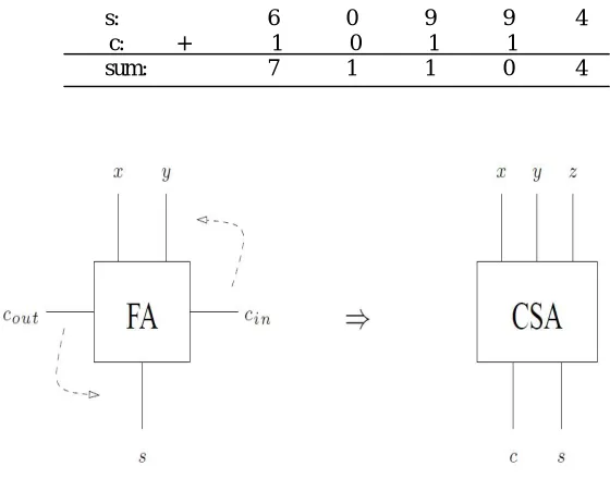
s: 6 0 9 9 4
c: + 1 0 1 1
sum: 7 1 1 0 4
Fig. 1 The Carry Save Adder (CSA) block and the Full Adder have same circuitry.
Fig. 2 One CSA block is used for each bit. This circuit adds three n = 8 bit numbers together into two new numbers. The important point which can be seen here is that c and s can be calculated individually and also each ci (and si) can be calculated individually from all of the other c’s (and s’s). In this way we can achieve our goal of converting three numbers that we wish to add into two numbers that add up to the same sum, and in O (1) time. The same logic can be applied and implemented on binary numbers. Which we can see using the below example:
x: 1 0 0 1 1
y: 1 1 0 0 1
z: + 0 1 0 1 1
s: 0 0 0 0 1
c: + 1 1 0 1 1
sum: 1 1 0 1 1 1
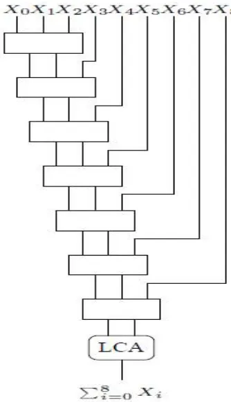
save adder is actually a full adder only but with the cin input renamed to z, the output z is renamed as s, and the output cout is renamed as c. Fig 2 shows how ‘n’ carry save adders can be arranged to add three n bit numbers x, y and z into two numbers c and s. It is also very important to note that the carry save adder block in the zero bit position generates c1 and not c0. Similarly the least significant column when we are adding numbers by hand, c0 will be equal to zero. All of the CSA blocks are actually independent, thus the entire circuitry takes only O (1) time. We still need a LCA to obtain the final sum, for which we require O (log n) amount of delay. The asymptotic gate delay for the addition of three n-bit numbers is in this way is the same as to add just two n-bit numbers. So to what extent does it take us to include m diverse n-bit numbers together? The straightforward methodology is just to repeat this process roughly m times over. This is shown in Fig 3. We have m − 2 CSA blocks wherein every block in the figure really shows numerous one bit CSA blocks in parallel, that we need to experience and after that the last LCA. Whenever we pass through a CSA block, the size of our number increases by one bit.
Fig. 3 Chain of CSA’s used to add m n-bit numbers
Fig. 4 A Wallace tree implementation to add m n-bit numbers.
IV.SIMULATION RESULTS
In this section the results obtained from simulation and the synthesis reports are presented. The aim was to design a highly efficient and low power 32-bit multiplier, which is of high speed and requires lower chip area. The simulation of the 32-bit multiplier is shown in this section. For the simulation process XILINX 13.2 and Modelsim 6.3 software’s were used. The simulation results show that our 32-bit multiplier takes less time to generate the final product and hence we can saw that the multiplier design using CSA consumes less power.
Fig. 6 32-bit Multiplier output result (inputs and output signals are shown in decimal for easy cross verification).
Fig 5 and Fig 6 show the waveforms of the 32-bit multiplier design. Fig 5 shows the inputs and the outputs in binary format, whereas for simplification Fig 6 shows the inputs and outputs in decimal format for easy verification.
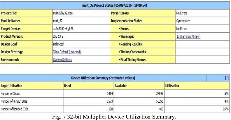
Fig. 7 32-bit Multiplier Device Utilization Summary.
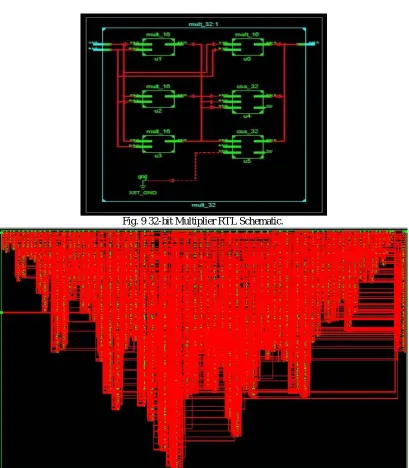
Fig 8: 32-bit Multiplier RTL Schematic.
Fig. 9 32-bit Multiplier RTL Schematic.
V.CONCLUSION
In this paper we present a 32-bit multiplier design which is highly efficient and low power consuming. The multiplication operation using carry save adder is faster and efficient than any other adder. From the results, we see how CSA logic is implemented in each partial product line which improves the overall performance of the multiplier unit. This multiplier is very much helpful in larger multiplications as the delay has been reduced. This design is implemented on 32-bit unsigned data. This design can also be extended over signed multiplication as well as it can be used for designing of higher bit multiplier.
REFERENCES
[1] Mariya Stephen, “Design for Low Power Multiplier Based on Fixed Width Replica Redundancy Block & Compressor Trees”, IJSR, Volume 4 Issue 10, October 2015.
[2] Vrushali gaikwad, Rajeshree Brahmankar, Amiruna Warambhe, Yugandhara Kute, Nishant Pandey, “32 Bit Parallel Multiplier Using VHDL”, IJETT, Volume 9 Number 3, March 2014.
[3] Prof. Loh, “ Carry Save Addition”, CS3220 – Processor Design, Feb 2005.
[4] Raminder Preet Pal Singh, Parveen Kumar, Balwinder Singh, “Performance Analysis of 32-Bit Array Multiplier with a Carry Save Adder and with a Carry Look Ahead Adder”, IJRTE, Volume 2 Number 6, Nov 2009.
[5] B. Parhami, “Computer Arithmetic, Algorithm and Hardware Design”, Oxford University Press, New York, pp. 91-119, 2000.
[6] Stephen Brown and Zvonko Vranesic,”Fundamentals of Digital Logic with VHDL Design”, 2nd Edn. McGraw-Hill Higher Education, USA.ISBN: 0072499389, 2005.
[7] Wakerly, J.F. “Digital Design-Principles and Practices”, 4th Edn, Pearson Prentice Hall, USA.ISBN: 0131733494.
[8] Rajender Kumar, Sandeep Dahiya, “Performance Analysis of Different Bit Carry Look Ahead Adder Using VHDL Environment”, IJESIT, Volume 2, Issue 4, July 2013. ISSN: 2319-5967.