© 2015, IJCSMC All Rights Reserved 978
Available Online atwww.ijcsmc.com
International Journal of Computer Science and Mobile Computing
A Monthly Journal of Computer Science and Information Technology
ISSN 2320–088X
IJCSMC, Vol. 4, Issue. 6, June 2015, pg.978 – 983
RESEARCH ARTICLE
Design and Implementation of Direct Mapped
Cache Memory with Same Tag Bit Information
Pavana Shree B. V, Mrs. Anitha V
Electronics and Communication Department, Visvesvaraya Technological University BELAGAVI, India
Electronics and Communication Department, DAYANANDA SAGAR COLLEGE OF ENGINEERING,Bengaluru, India
E-mail: [email protected]
E-mail: [email protected]
ABSTRACT: As L2 cache is large memory compared to L1 cache so the access time and power utilization will be high compared to accessing L1 cache. So the way-tag architecture needs to present in this cache architecture. In this paper, we propose a new cache architecture referred to as way-tagged cache to enhance the energy efficiency of L2 cache. The proposed method empowers L2 cache to work in an equal direct mapping manner. This leads to significant energy reduction without performance degradation. If the error identified in the location of L2 cache it should correct the error using same tag bit information. At the point when data are fetched from the main memory, it is checked if neighboring cache lines have the same tag bits as those of the data fetched. This same tag bit information is stored in the cache as additional bits to be utilized later. At the point when an error is recognized in the tag bits, the same tag bit information is utilized to recover from the error in the tag bits.
Keywords- Cache, Tag bits
I. INTRODUCTION
A cache is utilized by the central processing unit of a computer to reduce the average time to access data from the main memory. The cache is a smaller, faster memory which stores duplicates of the data from as often as possible utilized main memory locations. A small block of high speed memory called a cache between the main memory and the processor. Cache stores the recently accessed data so that the future requests for the particular data can be served faster.
The configuration of the L1 cache should be to maximize the hit rate, while keeping the cache latency as low as possible. The L2 cache is shared between one or more L1 caches and is frequently much, much larger. While the L1 cache is designed to maximize the hit rate, the L2 cache is designed to minimize the miss penalty.
© 2015, IJCSMC All Rights Reserved 979
cache line this phenomenon known as same tag bits. We utilize this same tag bits to correct the error in cache memory.
The input is driven from CPU. The input will first search to L1 block for cache hit/miss. Assume if L1 cache is hit, the data are accessed from L1cache so no need to search L2 cache. If the error recognized in the address of L1 cache it should correct the error using same tag bit information. Assume the address not accessible in L1 cache means definitely the address will search in the L2 cache. As L2 cache is containing large memory compared L1 cache so the access time and power consumption will be high compared to accessing L1 cache and also increases the number of ways accessed during L2 cache accesses. The proposed way-tagged cache exploits this fact to reduce the number of ways accessed during L2 cache accesses. If the error recognized in the address of L2 cache it should correct the error using same tag bit information.
II. RELATED WORK
W. Zhang [1], The fundamental thought of ICR is to replicate frequently accessed cache lines into other cache lines, which are predicted not to be accessed further, called dead blocks. Duplicated cache lines can be used to correct tag bits errors in the active lines. For this reason, we use a dead block prediction strategy, wherein blocks that have not been utilized used for a while are declared to be dead and their space in the L1cache is reused to keep up copies for the blocks in active use.
J. Hong [3], In this paper, they designed a four way set associative cache .When data are fetched from the main memory, it is checked if neighboring cache set have the same tag bits as those of the data fetched. This same tag bit information is stored in the caches as additional bits to be utilized later. When an error is identified in the tag bits by using parity method, the error can be corrected if the same tag bits were present in adjacent cache sets.
K. Bhattacharya [5], The authors have research in detail the multi-bit soft error rates in large L2 caches and propose a framework of solutions for their correction based on the amount of redundancy present in the memory hierarchy. In this methodology , basic error detection codes like hamming distance or cyclic redundancy codes are utilized to identify the multiple-bit errors, and they are corrected using the redundancy existing as part of the memory hierarchy.
W. Zhang[7], This paper proposes a cost-effective solution to enhance data reliability significantly with least effect on performance. The idea is to include a small fully associative cache to store the replica of every write to the L1 data cache. Because of data locality and its full associativity, the replication cache can be kept small while providing replicas for a significant fraction of read hits in L1, which can be utilized to enhance data integrity against soft errors. This fully associative cache is known as replication cache in this paper.
III. PROPOSED APPROACH
L1 block that is L1 cache contain two tag array and two data array that is 2-way set-associative memory. The input is driven from CPU, it will first search to L1 block for cache hit/miss. Assume if L1 cache is hit, the data are accessed from L1cache so no need for search L2 cache. If the error recognized in the address of L1 cache by parity method, it should correct the error using same tag bit information.
Assume the address is not available in L1 cache, implies without a doubt the address will seek in the L2 cache. As L2 cache is containing large memory compared L1 cache, so the access time and power utilization will be high compared to accessing L1 cache. So the way-tag architecture has to introduce in this cache architecture.
At the time When L1 cache miss happens, we need to access way tag array, if the way information’s of your address is available in way-tag array means you will directly access the L2 cache tag array by utilizing way-decoder. The way-tagged cache needs to send its way tag in the way-tag buffer. Way-tag buffer temporarily stores the way tags read from the way-tag arrays. A way decoder is utilized to decode way tags and generate the enable signals for the L2 cache, which activate only the desired ways in the L2 cache. The way-decoder will guide to access the tag array specifically. Assume the way information’s is not available means the cache works in conventional operation in L2 cache after that, the accessed way information’s are stored in way tag array.
© 2015, IJCSMC All Rights Reserved 980
© 2015, IJCSMC All Rights Reserved 981
This section discusses the results of the architecture designed. Proposed system is synthesized on Xilinx FPGA target device using Virtex 5. The device utilization summary is shown in TABLE. 1. As can been seen from the table, the proposed architecture utilizes 93 slice registers .TABLE.2 gives the comparison of the proposed architecture with the existing architecture in terms of Slice registers, Slice LUTs , Bonded IOBs. From the table, it is evident that the device utilization for the proposed design is lesser compared to the existing architectures.
Logic Utilization
Used
Available
Utilization
Number of Slice registers
93
28800
0%
Number of Slice LUTs
205
28800
0%
Number of Fully used LUT – FF
pairs
64
234
26%
Number of Bonded IOBs
29
360
8%
Number of BUFG/BUFGCTRLs
1
32
3%
Table.1 Device Utilization Summary
Architecture
Slice registers
Slice LUTs
Bonded IOBs
Conventional approach
8249
3884
34
Proposed Way tag array
93
205
29
Table.2 Comparison of various architecture with proposed system
© 2015, IJCSMC All Rights Reserved 982
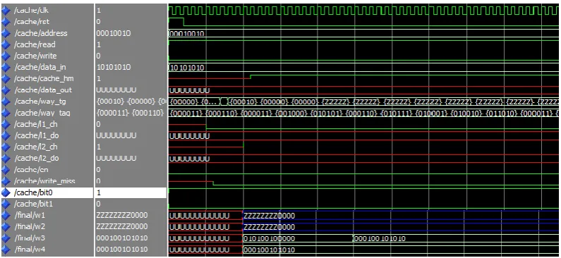
Fig 2. shows the L2 cache accessing as conventional way. If the error detected in the address of L2 cache it should correct the error using same tag bit information.
Fig.3. L2 cache access using Wag tag array
Fig.3 shows the L2 cache accessing by using way tag array. If the error detected in the address of L2 cache it should correct the error using same tag bit information
V. CONCLUSIONS
This paper exhibits a new energy-efficient cache technique for high-performance microprocessors. The proposed way-tagged cache reduces the number of ways accessed during L2 cache accesses. Using the way tags stored in the way-tag arrays, the L2 cache can be accessed as a direct-mapping cache. The idea of way tagging can be applied to many existing low-power cache techniques, for example, the phased access cache to further reduce cache energy consumption. Cache memories are vulnerable to transient errors because of their low voltage levels and sizes. It is becoming important to prevent transient errors and give a correction mechanism for hardware circuits. When an error is identified in the tag bits, the same tag bit information is utilized to recover from the error in the tag bits.
ACKNOWLEDGEMENT
Thanks to my Guide, friends and family member who always support, help and guide me during my dissertation.
REFERENCES
[1] W. Zhang, S. Gurumurthi, M. Kandemir, and A. Sivasubramaniam, “ICR: In-cache replication for enhancing data cache reliability,” in Proc.Int. Conf. Dependable. Syst. Netw., 2003, pp. 291–300.
[2] S. Mukherjee, J. Emer, T. Fossum, and S. Reinhardt, “Cache scrubbing in microprocessors: Myth or necessity,” in Proc. Int. Symp. Dependable Comput., 2004, pp. 37–42.
[3]J. Hong, J. Kim, and S. Kim “Exploiting Same Tag Bits to Improve the Reliability of the Cache Memories” IEEE, 2014.
[4] C. Slayman, “Cache and memory error detection, correction, and reduction techniques for terrestrial servers and workstations,” IEEE Trans.Device Math. Rel., vol. 5, no. 3, pp. 397–404, Sep. 2005.
[5] K. Bhattacharya, N. Ranganathan, and S. Kim, “A framework for correction of multi-bit soft errors in L2 caches based on redundancy,” IEEE Trans. Very Large Scale Integr. (VLSI) Syst., vol. 17, no. 2, pp. 196–206, Feb. 2009.
© 2015, IJCSMC All Rights Reserved 983 Dec. 2005.
[8] Jianwei Dai and L. Wang “An Energy-Efficient L2 Cache Architecture Using Way Tag Information Under Write-Through Policy” IEEE, 2012.