DOI: 10.15662/ijareeie.2014.0307038
Multi output Active Clamped Flyback
Converter
Aruna N S
1, Dr. S G Srivani
2, Balaji P
3,
PG Student [PE] , Dept. of EEE, R.V. College of Engineering, Bangalore, Karnataka , India1
Associate professor, Dept. of EEE, R.V. College of Engineering, Bangalore, Karnataka , India2
Deputy Engineer, Bharat Electronics Limited Bangalore, Karnataka , India 3
ABSTRACT: This paper presents the design of multioutput active clamp fly back converter topology which is operated at 100 KHz in CCM mode respectively. This provides output voltages (positive and negative), lower and higher voltages than input voltage. With the help of active clamp circuit, the transformer leakage energy is recycled, and zero-voltage-switching (ZVS) for primary main switch is achieved .
KEYWORDS: Multioutput, Active clamp flyback Converter, CCM (continuous conduction mode), zero voltage switching (ZVS)
I. INTRODUCTION
Power supplies are amongst the most popular part of electronic test equipment. It is a device that supplies electric power to an electrical load. Power supplies are used extensively in industrial application to meet the following purpose: (a)Isolation between the source and load; (b) Reduction of size and weight.;(c) Controlled direction of power flow; (d) High conversion efficiency; (e) Input and output waveform with a low total harmonic distortion for small filters; (f) Controlled power factor if the source is an ac voltage.
To achieve purpose switched-mode power supply are selected. These supplies include high frequency converter topologies to get improved performance and to realize in compact size,[1],[2]Compare to other topologies in flyback is simple, less components, low cost and it is used for low power application..So it is essential to design these supplies using high frequency converter topologies to get improved performance compact size, reduce the switching losses [3],[4].In this paper multi output active clamp flyback converter topology is presented.. In a flyback converter, when more than one output is present, the output voltages track the input voltage and the load, far better than they do in the forward converter. This is because of the absence of the output inductor, so the output capacitor connects directly to the secondary of the transformer and acts as a voltage source during the turned off period of the switch They are especially popular in multi-output applications, due to the low parts count one diode and capacitor per output. The switch in the flyback converter is operated at hard switching. Therefore the voltage and current stress of switch suffered from the transformer leakage inductance is very high and also an EMI problem from the hard switching limit the power rating for higher power application [5],[6]. To overcome these drawbacks, and to achieve ZVS, active clamp circuit is added. Active clamping is an effective means to clamp the voltages across semiconductor devices as well as to achieve soft switching [7]-[9]. The active-clamp circuit provides the benefits of recycling the transformer leakage energy while minimizing turn-off voltage stress across the power switch [10]-[11]. In addition, the active-clamp circuit provides a means of achieving zero-voltage-switching (ZVS) for the power switch and subsequent lowering of the output rectifier di/dt. This results in decreased rectifier switching loss and output switching noise.
DOI: 10.15662/ijareeie.2014.0307038
II. SYSTEM MODEL AND ASSUMPTIONS
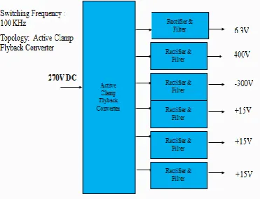
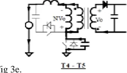
Fig 1: shows the block diagram of multioutput active clamp flyback converter. Fig2: shows the circuit configuration of the active clamp flyback converter. The magnetizing inductance is represented as Lm. The resonant inductance Lr is the sum of transformer leakage inductance and external inductance. The resonant capacitance Cr is equal to the parallel combination of the parasitic capacitance of main switch S1 and auxiliary switch S2. The auxiliary switch S2 and clamp capacitor Cclamp represent the active clamp circuit to recycle absorb the surge energy due to the leakage inductance so as to reduce the voltage stress of main switch S1. The resonant capacitance Cr and inductance Lr are resonant to achieve ZVS operation for main switch S1. Before the system analysis, some assumptions are made as: (1) The resonant period generated by the clamp capacitance Cclamp and resonant inductance Lr is greater than turn off time of main switch; (2) The resonant inductance is less than magnetizing inductance (Lr<<Lm); (3)All semiconductors (switches and diodes) are ideal; (4) The converter is operated in the continuous conduction mode; (5)the energy stored in the resonant inductance is greater than energy stored in the resonant capacitance in order to achieve ZVS operation for main switch.
Fig 1. Block diagram of multioutput active clamp flyback converter
Fig 2. Circuit configuration of the active clamp flyback converter
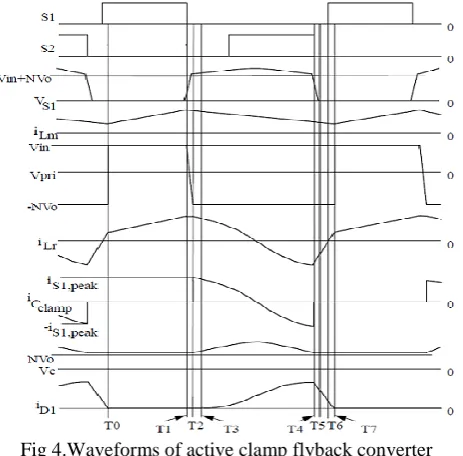
Fig (3a),(3b),(3c),(3d),(3e),(3f) and Fig(3g) shows necessary equivalent circuits for each interval and Fig (4) shows waveforms of active clamp flyback converter respectively .
DOI: 10.15662/ijareeie.2014.0307038
T0-T1: At T0, switch S1 is on, and the auxiliary switch, S2, is off. The output rectifier, D1, is reversed biased. The magnetizing inductance is being linearly charged as it charges in "normal" flyback operation.
Fig 3b.
T1-T2: S1 is turned off at T1. Cr is charged by the magnetizing current which is also equal to the current through the resonant inductor. The charge time is very brief, leading to an approximately linear charging characteristic.
Fig 3c.
T2-T3:At T2, Cr is charged to the point where the anti-parallel diode of S2 starts to conduct. The clamp capacitor fixes the voltage across resonant inductor Lr and the transformer magnetizing inductance to Vc (≈NVo), forming a
voltage divider between the two inductances,(where Vc is clamp voltage, N is turns ratio and Vo is output voltage). Since Cclamp is much larger than resonant capacitor Cr, nearly all of the magnetizing current is diverted through the diode to charge the clamp capacitor. Consequently, the voltage appearing across the magnetizing inductance, Vpri, decreases as Vc increases, according to the voltage divider action, Vpri=-Vc( Lm/Lr+Lm).
Fig 3d.
T3 - T4:At T3, primary voltage Vpri has decreased to the point where the secondary transformer voltage is sufficient to forward bias D1. The transformer primary voltage is then clamped by the output capacitance to approximately NVo. Lr and Cclamp begin to resonate. In order for S2 to achieve ZVS, the device should be turned on before clamp capacitor current Iclamp reverses direction.
Fig 3e.
T4 - T5: The auxiliary switch, S2, is turned off at T4, effectively removing Cclamp from the circuit. A new resonant network is formed between the resonant inductor and the MOSFET parasitic capacitances. The transformer primary voltage remains clamped at NVo as Cr is discharged.
DOI: 10.15662/ijareeie.2014.0307038
T5-T6: Assuming the energy stored in Lr is greater than the energy stored in Cr, At T5 Cr will be sufficiently discharged to allow S1’s body diode to start conducting. The voltage across the resonant inductor becomes clamped at Vin+NVo
Fig 3g.
T6-T7: S1 is on, and the secondary current is decreasing as the resonant inductor current increases. At T7, the secondary current decreases to zero (because the resonant inductor current has equalled the magnetizing current), and D1 reverse biases, allowing the polarity to reverse on the transformer primary. The magnetizing and resonant inductances begin to linearly charge again, starting another switching cycle (T7 = T0).
Fig 4.Waveforms of active clamp flyback converter
III. CIRCUIT DESIGN
Assumed that the maximum duty cycle of active clamp flyback converter is Dmax. The turn ratio between the transformer primary side and secondary side is equal to N = Np/Ns = [Vin min *Dmax/Vo(1-Dmax)].
If the clamp capacitance is large enough, the voltage across resonant inductor is neglected. Peak current of the main switch,
Is1,peak = {(Po total/ η Vin max Dmax)+(Vin min*Dmax*Ts/Lm)}
where, Ts is switching period,
Vin min is minimum input voltage, Po total is total output power, Ƞ is efficiency.
Voltage stress of rectifier diode
VD1,max = (Vin max/N)+Vo
Peak secondary diode current ID1peak =( 2Po/Vo*(1-Dmax))
Calculation of output capacitance
DOI: 10.15662/ijareeie.2014.0307038
where,Vout ripple = 1% of Vo, Fs is Switiching frequency.
Resonant capacitance : Cr=parallel combination of the parasitic capacitance of main switch S1 and auxiliary switch S2. So, Cr= 200Pf
Resonant inductor Lr is given by, Lr = ([1]/4π^2* fr^2*Cr).
Clamp capacitance is given by, Cclamp = [[1-D min vin)Ts]^2]/[П^2*Lr].
where, Dmin Vin=(Dmax Vinmin)/Vmax,min. With all these design factors keeping in mind we the design parameters are summarized as follows.
Designed parameters
Input Vin 270V+-1%
Output voltage Vout
6.3V/3.5A 400V/30mA -300V/30mA 15V/250mA 15V/250mA 15V/250mA
Po total 70W
Table 1: Design parameters
IV. RESULT AND DISCUSSION
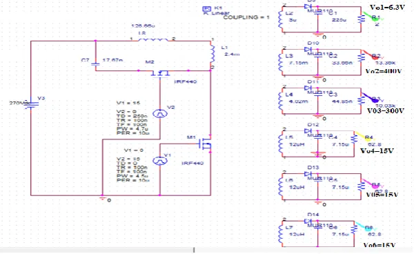
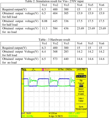
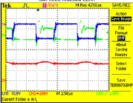
A 70W system parameters of converter are shown in table 1. Fig.5 shows simulation circuit of multioutput active clamp flyback converter respectively. Table 2 and 3 gives simulation and hardware results respectively. Fig.(6) and (7) shows the experimental waveforms of the gate-to-source voltages of main switch and auxiliary switch of main switch. The time delay between the auxiliary switch turn-off and main switch turn-on to ensure main switch turn on at ZVS respectively. Fig.(8) gives the experimental waveforms of gate signals of main switch Vs1,gs and auxiliary switch Vs2,gs and transformer primary voltage Vpri, Ipri. When main switch is turned on, the transformer primary side voltage is equal to Vin. If the main switch is turned off, the primary side voltage equals (-nVo). Fig. (9) shows the gate-to-source and drain- to source voltage for main switch. Before the mains switch is turned on the drain-to-source voltage has been reached zero. Fig. (10) gives the switch Vs1,gs and auxiliary switch Vs2,gs. and transformer experimental waveform of clamp capacitor voltage.
DOI: 10.15662/ijareeie.2014.0307038
Table 2: Simulation result for Vin= 270V input
Vo1 Vo2 Vo3 Vo4 Vo5 Vo6
Required output(V) 6.3 400 300 15 15 15
Obtained output voltage(V) for full load
6.5 404 305 15.9 15.9 15.9
Obtained output voltage(V) for half load
8.08 445 336 17.5 17.5 17.5
Obtained output voltage(V) for no load
11.3 584 436 23.69 23.69 23.69
Table : 3 Hardware result
Vo1 Vo2 Vo3 Vo4 Vo5 Vo6
Required output(V) 6.3 400 300 15 15 15
Obtained output Voltage(V) for full load
6.4 368 283 14.2 14.2 14.2
Obtained output Voltage(V) for no load
6.5 573 440 14.6 14.6 14.6
Fig 6 : the gate-to-source voltages of main switch(blue) in channel 1 and gate to source voltage of auxiliary switch(green) in channel 3.
DOI: 10.15662/ijareeie.2014.0307038
Fig 8: the gate-to-source voltages of main switch(blue) in channel 1 and gate to source voltage of auxiliary switch(green) in channel 3.Andthe transformer primary voltage Vpri(red) in channel 2 and primary current Ipri (pink)
in channel 4
Fig 9: the gate-source voltage (blue) of main switch, gate to source voltage of auxiliary switch(green) and drain- to-source voltage(red) of main switch. Before the mains switch is turned on the drain-to-to-source voltage of main switch
has been reached zero.
DOI: 10.15662/ijareeie.2014.0307038
V. CONCLUSION
The operation, functioning of 70W active clamp flyback converter for multioutput studied. The simulation circuit is designed and the required multioutput output voltages of 6.3V, 400V, 300V, 15V, 15V, 15V are obtained. The magnetizing and leakage energies are recycled and returned to the source. These benefits allow power converter designers to achieve ZVS and reduces voltage stress on switch.
REFERENCES
[1] Mohan, N., Undeland, T. M., and Robbins, W. P. “ Power Electronics: Converters, Applications and Design”. Third edition. New York: Wiley, 2012.
[2] Muhammad. H. Rashid.” Power electronics circuits, Devices, and Applications”, third edition. Pearson , 2011 [3] A. I. Pressman, “Switching Power Supply Design”, Mc Graw- Hill, Second Edition. 1999
[4] K. Billings, “Switching mode power supply handbook”, New York, 1989.
[5] H. S. -H. Chung, S. Y. Hui, and W. -H. Wang, “A zero-current-switching PWM flyback converter with a simple auxiliary switch,” IEEE Trans. Mar. 1999.
[6] A. Emrani, E. Adib, and H. Farzanehfard, “Single-switch soft-switched isolated DC-DC converter,” IEEE Trans. Apr. 2012.
[7] K. Yoshida, T. Ishii, and N. Nagagate, “Zero voltage switching approach for flyback converter,” in Proc. Int. Telecommun. Energy Conf. (INTELEC), 1992
[8] R. Watson, F. C. Lee, and G. C. Hua, “Utilization of an active-clamp circuit to achieve soft switching in flyback converters,” in Proc. IEEE. 1996
[9] G. Spiazzi, L. Rossetto, and P. Mattavelli, “Design optimization of soft switched insulated DC/DC converter with active voltage clamp,” in Proc. IEEE Industry Applicat. Soc. Annu. Meeting, 1996
[10] Analysis, design and implementation of an active clamp flyback converter 2005 IEEE