A Performance Comparision of OTA Based
VCO and Telescopic OTA Based VCO for
PLL in 0.18um CMOS Process
Krishna B. Makwana
Master in VLSI Technology, Dept. of ECE, Vishwakarma Enginnering College, Chandkheda, Gujarat, India
ABSTRACT:This paper describes a performance comparison of two Voltage Controlled Oscillator for Phase Locked Loop. OTA Based VCO and Telescopic OTA Based VCO for PLLs in a 0.18 μm digital CMOS process are designed and their performances are compared based on the measurement results. Measured performances shows that jitter and power consumption in Telescopic OTA Based VCO is reduced as compared to OTA Based VCO with wide frequency range. These designs are suitable to design low power and low jitter Phase locked loop.
KEYWORDS: Phase Locked Loop (PLL), Voltage Controlled Oscillator (VCO), Operational Transconductance Amplifier(OTA), low power,Jitter
I. INTRODUCTION
A CMOS Voltage controlled oscillator (VCO) is a critical building block in PLL which decides the power consumed by the PLL and area occupied by the PLL. VCO constitute a critical component in many RF transceivers and are commonly associated with signal processing tasks like frequency selection and signal generation. RF transceivers of today require programmable carrier frequencies and rely on phase locked loops (PLL) to accomplish the same. These PLLs embed a less accurate RF oscillator in a feedback loop, whose frequency can be controlled with a control signal. Transceivers for wireless communication system contain low-noise amplifiers, power amplifiers, mixers, digital signal-processing chips, filters, and phase-locked loops.[4]
Voltage controlled oscillators play a critical role in communication systems, providing periodic signals required for timing in digital circuits and frequency translation in radio frequency Circuits. Their output frequency is a function of a control input usually a voltage. An ideal voltage-controlled voltage oscillator is a circuit whose output frequency is a linear function of its control voltage.[4] Most application required that oscillator be tunable, i.e. their output frequency be a function of a control input, usually a voltage.
In recent years LC tank oscillators have shown good phase-noise performance with low power consumption. However, there are some disadvantages. First, the tuning range of an LC-oscillator (around 10 - 20%) is relatively low when compared to ring oscillators (>50%). So the output frequency may fall out of the desired range in the presence of process variation. Second, the phase-noise performance of the oscillators highly depends on the quality factor of on-chip spiral inductors.[4] For most digital CMOS processes, it is difficult to obtain a quality factor of the inductor larger than three. Therefore, some extra processing steps may be required. Finally, on-chip spiral inductors occupy a lot of chip area, typically around 200 *200-300 * 300 m^2, which is undesirable for cost and yield consideration.[4]
II. CIRCUIT DESCRIPTION
A. OTA Based VCO
The operation of OTA Based VCO is similar to the ring oscillator. Fig 1. Shows a Basic Concept of OTA Based VCO. Conventional ring oscillators are designed from an impair (n) number of digital inverters. Fig.1a shows this traditional topology for (n)=3. The proposed circuit needs only one single ended OTA and one simple CMOS inverter to provide oscillation. Two simple CMOS inverters have been added to generate a buffered digital output.[1]
.
Fig.1 a) Ring Oscillator b) Concept of OTA[1]
Our proposed clock generator (or digital oscillator) is shown in Fig.2. This ring oscillator is basically composed by the digital inverter inv_1 and a rail-to-rail OTA between X and Z nodes. The OTA simulates a unit gain voltage follower and replaces inv_A and inv_B in Fig.1a.[1] Here, unit gain voltage follower is performed by the current feedback between the OTA output node and the OTA input negative node.
B. Telescopic OTA Based VCO
A telescopic OTA based current controlled oscillators offer the desired characteristics that suits integration in a PLL system.
1) OTA Stage: The circuit diagram of single ended telescopic OTA is shown in Fig. 3. The NMOS transistors M0, M1 forms the input differential pair. M2 and M3 is the cascode device of the input pair.[3] They are biased to be in saturation for this current range.PMOS transistors M4 to M7 forms the single ended cascade current mirror load. The devices are sized to handle this current swing and reduce the overdrive voltage so that the output swing of the OTA is well enough to trigger the oscillations.[3] An OTA designed from a classical differential input stage of two MOS transistors (in saturate mode of operation) exhibits a transconductance GM proportiona to I0.
Fig 3. Telescopic OTA[3]
. Based on this previous consideration, the OTA slew-rates will also be proportional to GM. we propose to approximate the frequency of oscillation is proportional to root of I0. The oscillation frequency of the proposed ICDO can be controlled from the OTA DC bias current.
Fig 4.. Baising Circuit[3]
3)Inverter Stages: The circuit diagram of output stage with two inverters cascaded is shown in Fig. 5. The size of these inverters is kept minimum which improves the speed and reduces the chip area. CMOS transistors M8, M9 and M10, M11 are identical.[3]
To integrate this ICO in PLL system a V to I Converter stage should be preceded. A simple MOS device when operated in saturation region produces a current proportional to the input voltage. This change in drain current with respect to change in input votage is called transconductance.
Fig 5. Inverter stage[3]
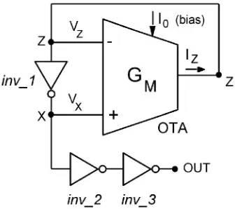
.A device with high transconductance converts small voltage change to large output current,which induces high frequency of oscillation in the designed ICO. The electrical representation of the proposed VCO block is shown in Fig. 6.
Figure 6 Voltage Control Oscillator[3]
III SIMULATION RESULT
A. Output Waveform
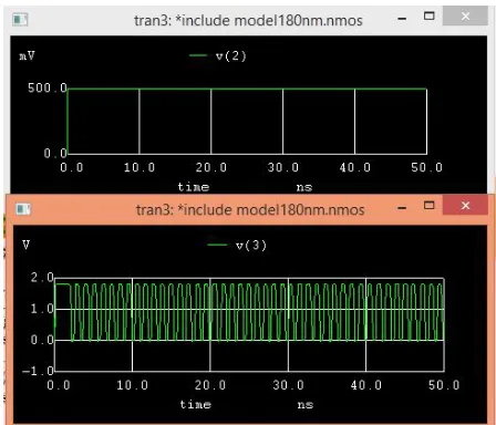
Figure 8 shows the output waveform of Telescopic OTA Based VCO when input control voltage is 1V. The output Frequency of VCO is 2890MHz.
Fig 8. Input and Output waveform of Telescopic OTA Based VCO
Fig.9
shows the graph of input voltage of VCO vs Output frequency of VCO. When the control voltage is varied from0V to 1.8V, the. Oscillation frequency of the designed Telescopic OTA Based VCO ranges from 2 MHz to 3000 MHz.. Gain of the VCO (KVCO) was calculated from the graph shown in Fig. 10, to be 2890 MHz/ V. It is also seen that the control voltage and output frequency vary linearly for a range of 430 to 1700 MHz. Thus the most suitable biasing of the PLL control voltage would be 0.4 V to 0.75V.
Fig.9 Frequency vs Control Voltage
B. Performance Comparision
tuning frequency range for PLL. Also the power consumption in Telescopic OTA Based VCO is reduced as compared to OTA Based VCO Shown in Table I.
TABLE I Measured Performance
IV CONCLUSION
This paper compares the performance of two VCO’s for PLLs, a current starved VCO and source coupled VCO with the design experiment and with the qualitative evaluation. Our measurement results show that in power consumption and tuneable frequency range, Telescopic OTA Based VCO is superior than OTA Based VCO.
ACKNOWLEDGEMENT
Any accomplishment requires the effort of many people and this work is not different. And it is my prime duty to acknowledge the person who directly or indirectly helped me. So,I take opportunity to heartly thank our project in charge respected Prof. NARESH PATEL for his valuable guidance and touch of inspirationand motivation throughout the work without whose help the work would not have been in the shape what it is. I am also thanking full to other relevant staff of workshop, library, and Department for their co-operation, help and guidance. I am also thankful to my co-colleagues for building good work to make the success of project.
REFERENCES
1. Herv Barthlemy, Stphane Meillre and Sylvain Bourdel, “ Single ended rail to rail CMOS OTA based variable frequency ring oscillator”,IEEE ISCAS,Vol 4, Page(s): 537-40, 2004
2. Gauri Shankar Singh, Devesh Singh, S.Moorthi,” Low Power Low Jitter Phase Locked Loop for High Speed Clock Generatio. Asia Pacific Conference on Postgraduate Research in Microelectronics & Electronics (PRIMEASIA), Page(s):192 – 196, ISSN : 2159-2144, December 2012.
3. S. Aditya_ and S. Moorthi_.”A Low Jitter Wide Tuning range Phase Locked Loop with Low Power Consumption in 180nm CMOS Technology” Asia Pacific Conference on Postgraduate Research in Microelectronics & Electronics (PRIMEASIA),IEEE, Pages:- 228 – 232, 2013
4. Rashmi K Patil, Vrushali G Nasre,” A Performance Comparison of Current Starved VCO and Source Coupled VCO for PLL in 0.18μm
CMOS Process”, International Journal of Engineering and Innovative Technology (IJEIT), Volume 1,Issue 2, February 2012. 5. Behzad Razavi, Design of Analog CMOS Integrated Circuits, International Edition, McGraw Hill publications, 2001. 6. “Operational Amplifiers”, Ching-Yuan Yang, National Chung-Hsing University, Department of Electrical Engineering. 2004.
Parameter OTA Based VCO
Telescopic OTA Based VCO Technology 0.18um 0.18um
i/p tunning range 0.65-1.2V 0.4-0.75V
Range of Oscillation Frequency
640-800MHz 400-1700MHz
Power
Consumption 0.32mW 5.14mW
![Fig 3. Telescopic OTA[3]](https://thumb-us.123doks.com/thumbv2/123dok_us/7790211.1290483/3.595.196.398.306.544/fig-telescopic-ota.webp)
![Fig 4.. Baising Circuit [3]](https://thumb-us.123doks.com/thumbv2/123dok_us/7790211.1290483/4.595.211.371.432.584/fig-baising-circuit.webp)
![Figure 6 Voltage Control Oscillator[3]](https://thumb-us.123doks.com/thumbv2/123dok_us/7790211.1290483/5.595.97.504.157.442/figure-voltage-control-oscillator.webp)