Modelling and Analysis of SET Effect in
Charge Pump PLL
Abhishek G M 1, Varsha Prasad 2
P.G. Student, Department of ECE, Nitte Meenakshi Institute of Technology, Bengaluru, Karnataka, India1
Assistant Professor, Department of ECE, Nitte Meenakshi Institute of Technology, Bengaluru, Karnataka, India2
ABSTRACT: In this paper we analyse the effect of Single event effect (SEE) in charge pump phase locked loop and the responses with different aspects such as voltage and current with respect to time. We demonstrate this impact of Single event transient (SET) effect on the charge pump circuit by modelling in matlab and Simulink tool. This SET effect has an impact on settling time, pulse width and frequency of the synthesized signal. A SET pulse of small amplitude and period is generated and tested for the modelled circuit examining the settling time and impacts of this pulse is studied. This generated pulse is tested before the low pass filter unit, Charge pump and for the Voltage controlled oscillator unit. The obtained responses are figured out and studied which will be further helpful for the radiation hardening of the system respectively. This is modelled using the MATLAB and SIMULINK tool.
KEYWORDS: Charge Pump (CP), Phase Locked Loop (PLL), Single Event Transient (SET), Voltage Controlled Oscillators (VCOs), Phase Frequency Detector (PFD).
I. INTRODUCTION
Electronic gadgets utilized on shuttle must be shielded from the impacts of radiation. This method of shielding the devices from the radiations of the externals is known as radiation hardening. The examination of the impacts of radiation on test PLLs demonstrates the simple escalated outline of a customary charge pump based PLL is not reasonable for radiation hardening applications. Frequency synthesizers are crucial building obstructs in wave frequency, correspondences, and simple sign handling for producing high precision wave signs. A case study of clementine failure, in which an noise caused due to the asteroid hit the device, which was very small in fact had a huge impact in the synthesis of the signal at the receiver part which led to the loss of data eventually failure of the device. Hence this study is helpful in analysis those effects on the system which is can be resourced to design radiation hardened system in further work.
II. RELATEDWORK
III.PROPOSED SYSTEM
The simple circuit of charge pump PLL comprised of the Phase Frequency-detector circuit for phase detection which has a feedback from the divider which is as shown in the figure. The system also comprises of the charge pump which converts voltage to current pulses.
A. Overall Structure of CP PLL
Fig. 1 Proposed Charge Pump PLL
The figure above represents the conventional charged pump PLL block diagram, which constitute of the Phase Frequency Detector (PFD), Charge Pump (CP) circuit, Loop Filter, Voltage controlled oscillator (VCOs) and the Frequency Divider Circuit. This circuit is modelled for the analysis of the SET effect on the system. The charge pump circuit senses the changes in voltage converting it to the current pulses. The VCO governs the frequency agility of the circuit.
B. Charge Pump model
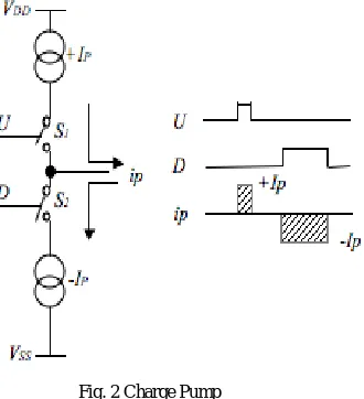
The Charge pump model comprises of an arrangement of current sources with sizes of IP1 and IP2 amps separately. As a rule the present sources are symmetrical in this manner IP1 = IP2 = IP. These are connected to the source and the ground respectively which acts as the sink as shown in the figure.
Fig. 2 Charge Pump
signal from the PFD which when fed, the upper signal leads to the positive current pulse, charging the capacitor at the loop filter and the down signal leads to the negative current pulse, eventually discharging the capacitor at the loop filter to the ground. These are activated by the switched S1 and S2 shown above. These switches both will never be ON. This enhances pumping the current into the filter, hence the name.
Fig. 3 Phase model of Charge Pump
When QA is high the capacitor charges and discharges when QB is high as shown in the above diagram. The
resultant curve is the difference of the signal pulse obtained.There are many types of Charge Pumps available namely,
Conventional Tri-Stage
Current Steering
Differential input with Single-Ended output
Fully Differential charge pumps
Which are based on the power consumption, speed, clock skew, Power and also based on clock generator. There are many non-idealities in charge pump like leakage current, mismatching of timing and charge sharing, etc. though there are many advantages of the charge pump as it devours less power than active filters, and has less noise comparatively. It is better with the objective of putting the loop filter in the chip.
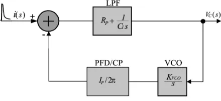
C. SET analysis for the voltage response
The below block shows the modelled Charge pump for which the small current pulse i(s) is provided indicated below
Fig. 4PLL model for SET characterization
Here IP is the charge pump current, KVCO is the gain of the VCO, RP is the resistance of the loop filter and
C1 is the capacitance of the loop filter and C2 is very less comparatively which can be neglected. Transfer function
H(s) =Vc(s) i(s)
H(s) = s(RpC1s + 1)
s2 + RpC1s +
On substitution we get the primary output of VC, as illustrated below,
Vc(t) = Ip∗Rp(e fτ(t)−e ( )fτ(t−T))
Where ( ) varies with the , as shown in the simulated results, the transient VC responses by varying
the pulse width (T), and by varying w.r.t the SET pulse amplitude IP and by varying the settling time constant
is mentioned in the simulated result.
Fig. 5 Transient VC response as a function of T, IP and settling-time constant τωn
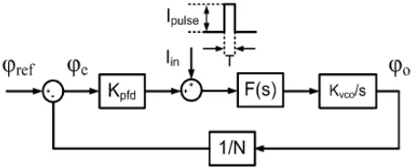
D. SET Analysis for the Error Response
The below block shows the current pulse Ipulseof small magnitude impacting on the PFD/CP, which also
excites the VCO output of the same. The error response is plotted by using the below mentioned transfer function and using the tool matlab and Simulink the response is obtained as follows.
The transfer function for the same is given by,
φe Iin(s) =
KvcoF(s)
Ns + KpfdKvcoF(s)
In time domain the current equation is given by
Iin(t) = IPulse* (u(t) – u(t-T))
Laplace transformation of the same is
Iin(s)= ( − )
For the error function the reverse Laplace transformation is applied to get the following error response equation as follows,
( ) = − − −
− − ∗{ ( )− ( − )}
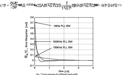
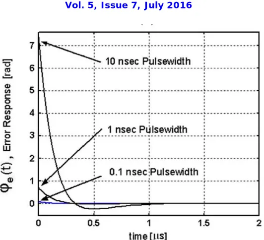
Fig. 7 Error response for different band width
Fig. 8 Error response for different pulse width
E. SET analysis for the Output Voltage
The below model is designed and the SET pulse i(s) is provide before the VCO block diagram as shown and characterised.
Fig. 9 PLL model for output characterization
The SET signal is of very small magnitude and of the time period 1ms. The impact of the same is measured and plotted accordingly. The transfer function of the output voltage Vc(s) varies w.r.t the pulse i(s), and is calculated as
G(s) = Kvco/s
The above equation G(s) shows the open loop transfer function, the overall equation for H(s) is given by
H(s) = ( )
( )=
∗
On simplification the Output is found to be,
V(s) = ∗( )
∗ ∗( / )
Where,
I(s) = Iset(1/s - / )
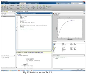
The model designed and conclusions are affirmed by simulations done utilizing the tool Simulink and matlab codes are also being synthesized. The simulation result of the PLL is a shown in the following figure.
Fig. 10 Simulation result of the PLL
IV. CONCLUSION
From the above experiment and analysis we understand the effect of SET behaviour on thedifferent stages of the component on the system. If this small pulse has a huge impact on the overall output, hence from the study, in order to mitigate this effect, optimization of the parameters such as RP, ζ, ωn, T, is necessary. And this study is beneficial
in further building the radiation hardened circuits by the analysis and effectively choosing the component parameters.
REFERENCES
[1] HoonHee Chung, Wenjian Chen, BertanBakkaloglu, Hugh J. Barnaby, Bert Vermeire, and SayfeKiaei, “Analysis of Single Events Effects on Monolithic PLL Frequency”, IEEE Transactions On Nuclear Science, Vol. 53, No. 6, December 2006.
[2] Zhao Zhenyuy, Li Junfeng, Zhang Minxuan and Li Shaoqing, “Modeling and analysis of single-event transients in charge pumps”,Computer School, National University of Defense Technology, Changsha 410073, China.
[4] F. M. Gardner, “Charge-pump phase-lock loops”, IEEE Trans. Cammun., vol. COM-28, pp. 1849-1858, Nov. 1980.
[5] Li Zhiqun, Zheng Shuangshuang and HouNingbing, “Design of a high performance CMOS charge pump for phase-locked loop synthesizers”, Journal of semiconductors, Vol. 32, No.7, July 2011.
[6] Anantha Nag Nemmani, Martin Vandepas, Kerem Ok, KartikeyaMayaram and Un-Ku Moon, “Design Techniques For Radiation Hardened Phase-Locked Loops”, School of Electrical Engineering and Computer Science, Oregon State University, Corvallis, OR 97330, July 2004. [7] Floyd M. Gardner, “Phase Accuracy of Charge Pump PLL’s”, Fellow, IEEE.
[8] T. D. Loveless, L. W. Massengill, W. T. Holman, B. L. Bhuva, “Modeling and Mitigating Single-Event Transients in Voltage-Controlled oscillators”, IEEE TRANSACTIONS ON NUCLEAR SCIENCE, VOL. 54, NO. 6, DECEMBER 2007.
[9] R. Koga, S. D. Pinkerton, S. C. Moss, D. C. Mayer, S. Lalumondiere, S. J. Hansel, K. B. Crawford, and W. R. Crain, “Observation of single event upsets in analog microcircuits,” IEEE Trans. Nucl. Sci., vol. 40, no. 6, pp. 1838–1844, Dec. 1993.
[10] M. W. Savage, T. L. Turflinger, J. L. Titus, H. F. Barsun, A. L. Sternberg, Y. Boulghassoul, and L. W. Massengill, “Variations in set pulseshapes in the LM124A and LM111,” in IEEE NSREC 2002 RadiationEffects Data Workshop Record, 2002, pp. 75–81.
[11] Y. Boulghassoul, S. Buchner,D.McMorrow, V. Pouget, L. W. Massengill, P. Fouillat, W. T. Holman, C. Poivey, J. W. Howard, M. Savage, and M. C. Maher, “Investigation of millisecond-long analog singleevent transients inthe LM6144 op amp,” IEEE Trans. Nucl. Sci., vol. 51, no. 6, pp. 3529–3536, Dec. 2004.