1-1-1966
The design of a hardware symbol table for use in an algebraic
The design of a hardware symbol table for use in an algebraic
computer.
computer.
Williams D. McGee University of Windsor
Follow this and additional works at: https://scholar.uwindsor.ca/etd
Recommended Citation Recommended Citation
McGee, Williams D., "The design of a hardware symbol table for use in an algebraic computer." (1966). Electronic Theses and Dissertations. 6433.
https://scholar.uwindsor.ca/etd/6433
THE DESIGN OF A HARDWARE SYMBOL TABLE
FOR USE IN AN ALGEBRAIC COMPUTER
BY
WILLIAM D. McGEE
„ A Thesis
Submitted to the Faculty of Graduate Studies through the Department of Electrical Engineering in Partial Fulfillment
of the Requirements for the Degree of Master of Applied Science at the
University of Windsor
Windsor8 Ontario
INFORMATION TO USERS
The quality of this reproduction is dependent upon the quality of the copy
submitted. Broken or indistinct print, colored or poor quality illustrations and
photographs, print bleed-through, substandard margins, and im proper
alignm ent can adversely affect reproduction.
In the unlikely event that the author did not send a com plete m anuscript
and there are missing pages, these will be noted. Also, if unauthorized
copyright material had to be removed, a note will indicate the deletion.
®
UMI
UMI M icroform EC52614Copyright 2008 by ProQuest LLC.
All rights reserved. This m icroform edition is protected against
unauthorized copying under Title 17, United States Code.
Approved
cized control, and input-output statements* The
problem of gaining access to memory,by means of the
symbolic addresses in the program, remains*
This Thesis presents three proposals for reducing
translation time. All three solutions require a hardware
table which is fast in its operation. This Thesis
presents the design of a table utilizing electrically
alterable, non-destinctive read-out, magnetic devices*
ACKNOWLEDGEMENTS
The author wishes to express his thanks to Dr,
P.A.V. Thomas, who supervised this work, for his helpful
suggestions and guidance.
The author is grateful to the Research and
Development Labs of Northern Electric Company Limited,
in Ottawa, for supplying the cores used in this design.
Acknowledgement is also due the National Research
ACKNOWLEDGEMENTS ... .
TABLE OF CONTENTS ...
LIST OF FIGURES ... .
I. INTRODUCTION ... ...
II. ALGEBRAIC COMPUTER ...
III. POSSIBLE SOLUTIONS
3.1 Proposal 1: A Fast Translation Before Execution ... 3.2 Proposal 2: Access By Symbolic Address 3.3 Proposal 3: Fast Translation During
Execution ... 3.4 Conslusions ... .
IV. SYSTEM DESIGN
4.1 Preliminary Specifications ... 4.2 The Basic Unit - A Multiaperture
Magnetic Device .... 4.3 The Two Stable States ... 4.4 Interrogating The Core ... 4.5 Core Characteristics ... ... 4.6 Machine Address Memory ... 4.7 Machine Address Memory Read Circuitry
4.S Symbolic Address•Memory ...
4.9 Writing Into The Symbolic Address
Memory ... ...
4.10 The Inhibit Winding... ... 4.11 Writing Into The Machine Address Memory 4.12 Restoring The Machine Address Memory
V. THE TEST M O D E L ... ... .
VI. RECOMMENDATIONS AND CONCLUSIONS .
BIBLIOGRAPHY... ... .
VITA AUCTORIS... ... ... ...
LIST OF FIGURES
figure Page
1. The Hardware Symbol Table ... 5
2. Flowchart of Translation Process ... 7
3. Access By Symbolic Address ... 9
4. A Multiaperture Magnetic Deyice ... 14
5. The Two Stable States 14 6. The Interrogation, Restore, and Output Windings ... 16
7. Read Cycle - Unblocked C o r e ... ... 16
S. Read Cycle - Blocked Core ... IB 9. Hysteresis L o o p ... IB 10. Core Characteristics ... 20
11. Machine Address Memory Output Lines ... 25
12. MAM Read Circuitry... 27
13. Timing of Strobe Pulse ... 29
14* Core Arrangement in S A M ... 31.
15* SAM Write Circuit ... 33
16. Writing a *1* ... 34
17. Writing a *0’ ... 34
IB. The Inhibit Winding... 36
19. Effect of Inhibit on Non-selected Cores . 36 20. Common Unblock Line ... 37
21. The Test M o d e l ... 40
1964, a study of the feasibility of building an algebraic
computer. The proposed machine would execute, directly,
instruction similar to those comprising Fortran and Algol
The great advantage to having such a computer is that no
compiling would be necessary and the program would be
executed immediately after being loaded into memory.
One of the major design problems is the method of
gaining access to memory. In this thesis, three possible
solutions to the problem are described and the reasons
for requiring a hardware table given. The remainder of
the thesis is devoted to the design of the table and a
prediction of its performance based upon the test results
II. ALGEBRAIC COMPUTER
It is the nature of the proposed algebraic com
puter that it have, as its machine language, mathematical
statements, such as SUM = X + Y, and anglicized control
statements, such as GO TO 123, as found in Fortran -
Algol type languages. With this property, compiling -
the translation of algebraic statements into a series of
conventional computer machine language instructions - is
eliminated. However, the symbolic addresses, whether
variable names, such as SUM, X and Y in the above example,
or statement labels,such as 123 above, remain to be
indentified with actual memory locations. In conventional
computers, a symbol table, which equates symbolic
addresses to machine addresses, is created in memory and
before execution begins, all symbolic addresses in the
program are replaced by their machine address equivalents.
This replacement consumes a considerable amount of time,
a good deal of which is spent searching the symbol table.
The reduction of symbolic address replacement time,
hereafter called translation, can be realized by either
eliminating the need for translation altogether, or con
structing a hardware table which will compare a symbolic
address to the entire collection of symbolic addresses
which occur in the program, and automatically give the
Ill POSSIBLE SOLUTIONS
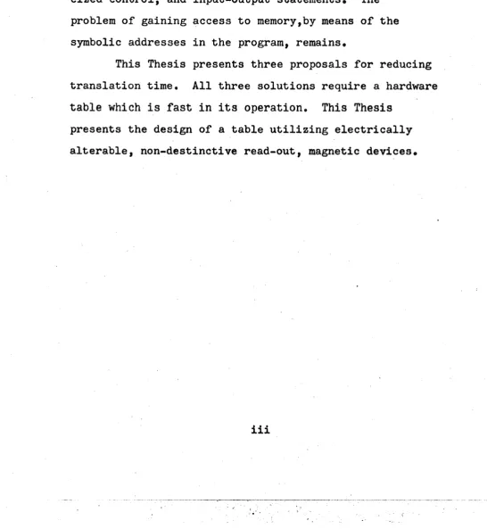
3.1 Proposal 1: A Fast Translation Before Execution
One means of reducing translation time is a
modification of the translation process of conventional
computers. The difference is that the symbolic addresses
and corresponding machine addresses are stored in a hard-
ware table rather than in main memory. See Figure 1.
While the program is being read into main memory,
the symbol table is constructed in the hardware table
with a one to one correspondence between the symbolic
addresses and machine addresses. Immediately after read
ing the program into main memory, the computer selects
the symbolic addresses from the program sequentially and
interrogates the table via the symbolic address register.
The operation of interrogation automatically compares the
contents of the symbolic address register (SAR) with
every symbolic address in the symbolic address memory
0AM) simultaneously, and energizes only the machine
address memory (MAM) read line which corresponds to an
equal compare in the SAM. The result of the MAM read
is the entering of the machine address equivalent to the
symbolic address in SAR, into the machine address
register (MAR).
>
o
< c5
Ll)
s
<X
1
1 u
1 > -1 1 O l i i 1 £ &
1 Ul 1
1 7 A. F -o £ o
I
]
main meMofcV
flcc&s
R ^ .^ S Sf r
O IX)
S AM ACCe&S Re&tSTc#
The machine address is now entered into the
program in main memory in place of the symbolic address.
Assume for the moment that the main memory is
organized in 6-bit bytes, and that there are several
bytes per word. Assume also that the main memory contains
4096 words. The memory is then addressable by a 12 - bit
address, i.e. 2 bytes. All single character (1 byte)
symbolic addresses must be converted to 2-byte machine
addresses upon translation and thus an extra byte must be
made available during storage of the program for the
extra byte required. See Figure 2 for a flow chart of
translation operation.
The SAM and MAM need only be large enough to
accommodate the largest number of different symbolic
addresses in the program. This ndmber is considerably
smaller than the number of words in main memory.
The use of the hardware table eliminates the need
for searching through a symbol table one comparison at a
time.
One disadvantage of this scheme is that the program
stored in main memory no longer contains symbolic addresses,
which are very useful in debugging the program.
This scheme requires logic capabilities beyond
those involved in the execution of the program. In
M
id
o
OL
U)
V
UJ cO
H
2 P
U
i p
4 ° J >2i«
(— ku
o
m£ 3 g *
</> i o
< o
-2 v»
r v» v
r
t
^ -: in
{g'Zli) < oi
CL I 5
io '“L °
U)0-*-p Oi O'* (L
6
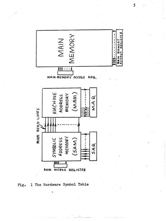
3.2 Proposal 2: Access By Symbolic Address
Another method of reducing translation time is to
have associated with the main memory, the symbolic
address memory (SAM), as described in Proposal 1. In
this scheme, there is a one to one correspondence between
the words of the SAM and the words in the main memory.
See Figure 3. In this scheme, no translation is necessary.
Every word in main memory is accessible by its symbolic
address which is assigned when the program is loaded. The
main memory must also be accessible by conventional machine
address means, because the program must be loaded and
executed sequentially.
This system, comprising the symbolic address
memory directly connected to the main memory, constitutes
a hardware table, as described in Proposal 1.
The great advantage of this system is that no
translation whatsoever is required. During the loading of
the program into main memory, the statement labels are
loaded in the SAM word corresponding the the word in main
memory in which the statement starts. At the samfe time,
variable names are loaded into the SAM starting at the
last word and working back. The instant loading of the
program is complete, execution can begin.
The great disadvantage of the system is in its
s m
f\CC ESS
R£Gr(&T£ft
MA
1W fflEMDfeVACCESS REGISTER
M A I N
MFMOftV
r , k
MfhiK) merrtOdY '
o u t p o t f t e 6 « s r e « 5 /» ftFig. 3 Access By Symbolic Address
10
statements in a program have a label, thus a large per
centage of the SAM is unused during execution of a given
program. Because of its size, and the special circuitry
required for its implementation, the cost of constructing
this system would be very high*
3.3 Proposal
J:
Fast Translation During ExecutionA third method of solving the problem of reducing
translation time is quite similar to Proposal 1. The
system requires a hardware table as described in Proposal
1. The table is loaded with symbolic addresses and
machine addresses as in Proposal 1; but, instead of
replacing the symbolic addresses in the program, the
table is consulted every time access to memory by symbolic
address is required. The machine address is then used
to retrieve or enter information into the main memory.
The symbolic addresses remain intact in the
program but the symbol table must be interrogated every
time a symbolic address appears for execution. While
the time required to retrieve the machine address is
small, the total time spent consulting the table can
accumulate to a significant value.
3.4 Conclusibns
All of the above proposals require some form of
IV. SYSTEM DESIGN
4*1 Preliminary Specifications
The symbolic address memory must be of course
capable of storage, but more specifically, must be of
the electrically alterable non-destructive read-out
(NDRO) type. The latter specification is necessary
because the entire SAM is interrogated at once, and the
information read from the SAM is not stored.
The SAM must also be capable of executing the
Boolean function, EXCLUSIVE-OR. That is, the output of
each SAM word must indicate whether or not the word is
exactly the same as the contents of the SAR.
The machine address memory need not be of the
NDRO type, although its use simplifies the read cir
cuitry.
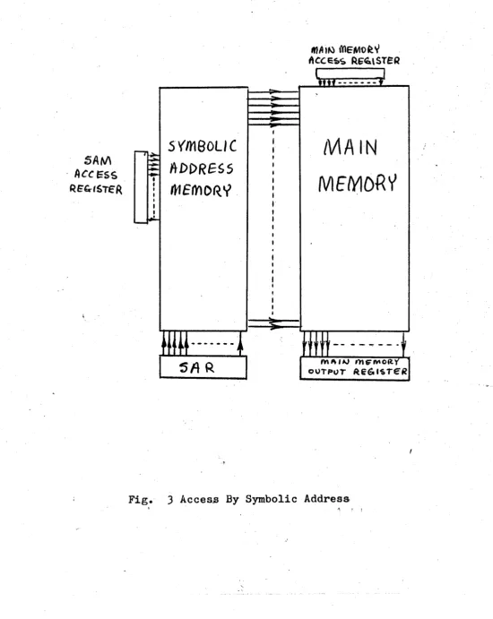
4.2 The Basic Unit - A Multiaperature Magnetic Device
A multiaperature magnetic core most hlosely
fulfils the required specifications. Flip-flops are
still too expensive to use on such a large scale, and
the logic required to perform the exclusive-or function
would make the cost prohibitive.
*
There are several electrically alternable NDRO
consists of a major aperature, Al, and four minor
apertures, A2, A3, A4 and A5. It is constructed so
that the minimum cross sectional area of the legs,
L2 and L3» about the minor apertures, is one-half the
cross sectional area of the major legs (11).
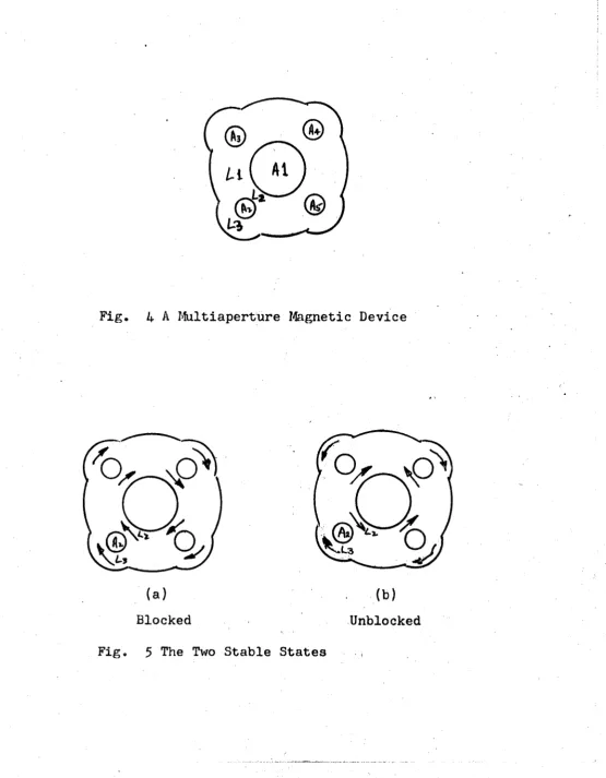
4.3 The Two Stable States
The two states of the core are called the blocked
i
state and the unblocked state.
If the remanent flux in the core is everywhere in
the same rotational direction about the major aperture,
and of such a density as to saturate the core, then it
is said to be in the blocked state. See Figure 5a.
If the remanent flux in the core is divided, such
that half is directed clockwise about the major aperture,
and half counterclockwise, and of such a density as to
saturate the legs about the minor apertures, then the
core is said to be in the unblocked state. See Figure 5b.
4V4 Interrogating The Gore
The core is interrogated by an attempt to switch
the direction of the flux about a minor aperture. The
14
Fig. 4 A Multiaperture Magnetic Device
(a)
Blocked Unblocked
then there is no flux change and hence no output.
If the core is unblocked, as in Figure 5b, and an
interrogating field of is applied to leg L3, then the
flux about the minor aperture A2 is switched and a
positive voltage pulse appears at the output. The core
is left in the unblocked state, but the flux about A2 is
in the counterclockwise direction. If another interroga
tion of the core were made, the output would be zero;
thus the flux direction about the minor aperture must be
restored to its original state, i.e. the clockwise diredt-
ion.
The restore field, which is of the same strength
as the interrogation field, is applied by another winding
on leg L3. The read cycle wave forms and core states
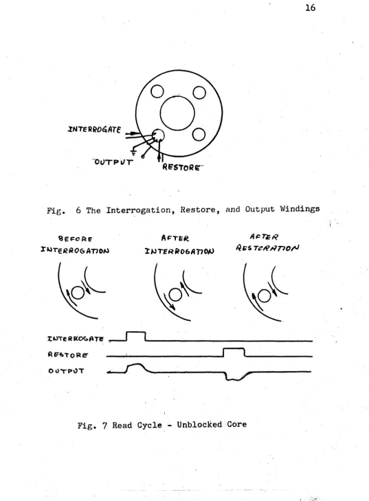
for the unblocked case are shown in Figure 7.
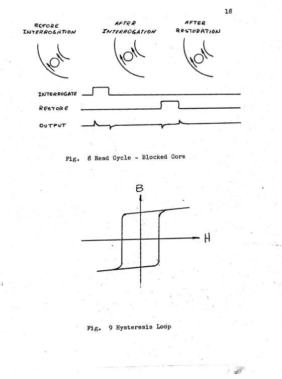
If the core is blocked, as in Figure 5a, and the
same read cycle is used, the field applied to leg L3
attempts to reverse the flux in L3« The flux in L2 is
already saturated counterclockwise about A3# thus a
different path must be found. The alternatetis around
the major aperture Al, a much longer path. If is
made large enough to reverse the flux around a minor
16
Fig. 6 The Interrogation, Restore, and Output Windings
IlOTeRKOGAre
fimoRe"
o o y p o t
and states. Likewise, when the restore field is applied,
there is no change of flux in L3 and the core is left in
its original state - blocked
Both the blocked and unblocked cores give a noise
output, because the hysteresis loop is not perfectly
rectangular. See Figure 9« With the application of the
interrogate field, there is a slight change of flux in
the core, which produces a noise spike at the beginning
of the pulse, and at the end. It is necessary, therefore,
to operate the core with interrogate and restore fields
which maximize the resolution between the two possible
outputs. The optimum fields can be determined from the
core characteristics.
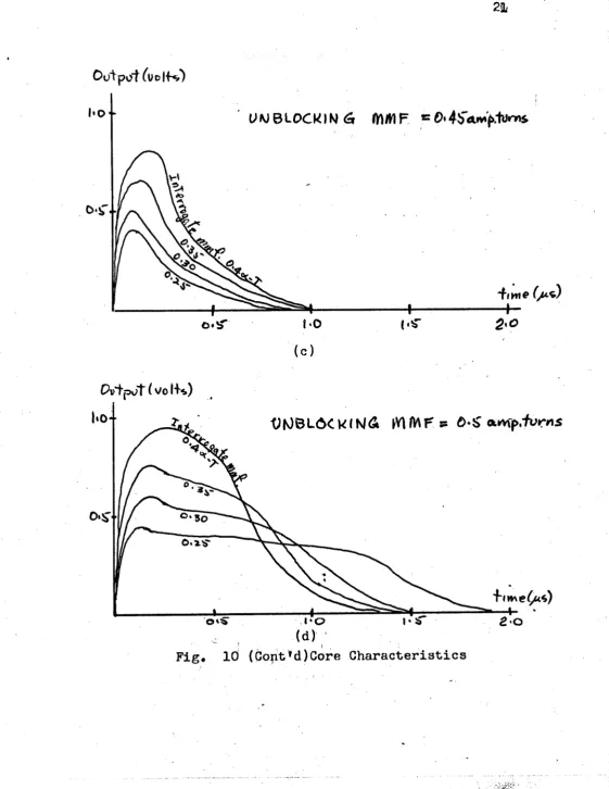
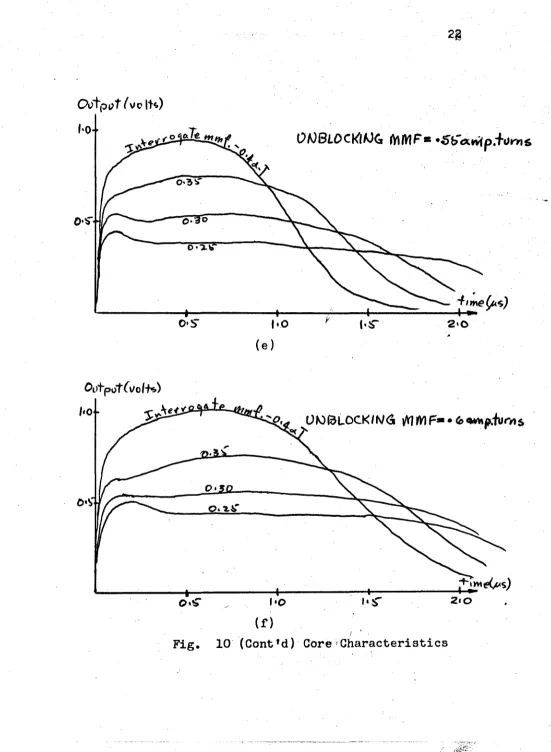
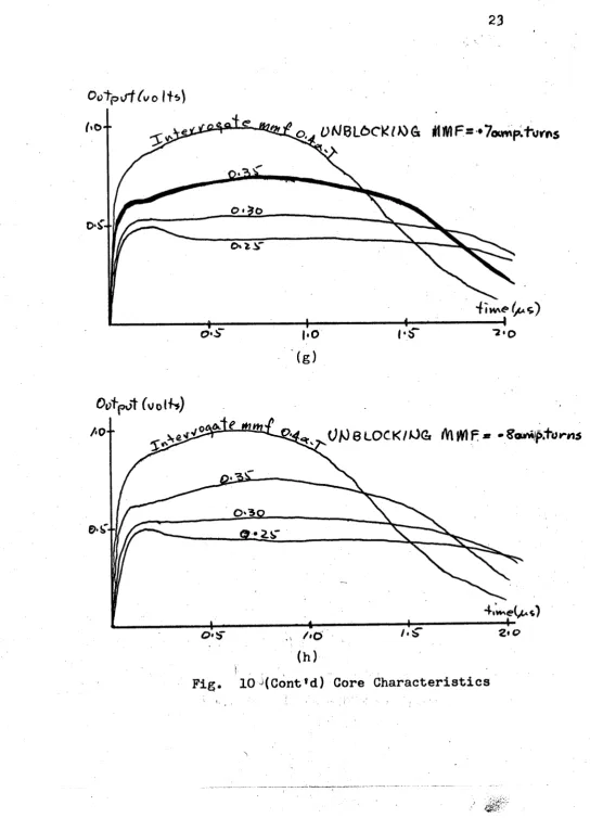
4.5 Core Characteristics
A set of typical core output characteristics were
collected in order to determine the optimum interrogation,
restore and unblocking fields. The output characteristics
are shown in Figure 10, and a discussion of them follows.
The core is set to the blocked state by the
application of an mmf large enough to produce saturat
ion in the same rotational direction about the major
lMTF/?/90<S/47>0A/
AFre/5
T*/T£/Q#0<£,A
Trot/
A F T S G
ResrrogATyoAJ
iJOTEftftOfiATc
i?FSTO (ie i --- j ~ i
o u t p u t
Fig. B Read Cycle - Blocked Core
B
H
reverse the direction of half the flux in the core. The
core characteristics show that the output is identical
for unblocking fields of .6 amp.-turns or greater, as
shown in Figure lOf through 10H. On this basis, the un
blocking mmf is chosen to be .7 amp.-turns.
The core can be set to the unblocked state by the
interrogation field, if it is large enough; thus the
interrogation field must be kept low enough so as to have
no effect on the flux about the major aperture, i.e.
less than .4 amp.-turns.
An interrogation field of .35 amp.-turns is chosen
in order to give a large and relatively flat output for an
unblocked core, and a relatively small noise output for
a blocked core. It is to be noted that 1.0 micorsecond -
after the interrogation field is applied, the noise
output decays to approximately 10 mv. for a blocked core.
4.6 Machine Address Memory
The machine address memory (MAM) can be constructed
20
1*0
UNBLOCK IM G
W M ? ~ Oampti
L>r*s1*0
(a)
Otftpot(\jo l-K)
UM© LOCK I MG M M F = 0 -4 ^
h o
(b)
UW BLOCkIM <k mmF * £• 4bWf>tu™s
t-0
(c )
Output
(
Vo Its)U N )B L6C klM & M M F ss d>-S **vfp. t v r n s
time£a*)
&c>
2g
Output A/c IH)
OAJSlOCklAJG flUVjF**
•&&"txriip,i'Oirn&
2*0
*
(e)
OotpotCvol'h’)
fro-U K ) B
l o c k i n&
m m f - •<*>«** v»s•o
(f)
Oo"fp\ft
(v
o
1t*)uN%i.d>c)fZiK>(a m f * +
(g)
£VfpJt
(voi'f'*)
0 ^ 8 L O C K / O G MjVIP* -Sa*vi)p.+orris
AO
(h)
24
destructive read-out element, such as the multiaperture
device described above, eliminates the need to rewrite
the information back into the memory after it has been
read-out. The design of this part of the hardware table
makes use of the NDRO element described in Section 4*4
It is the purpose of the SAM to select the word in
the MAM which is to be read. The design of the SAM is
given in a later section, so it is assumed here that a
word has been selected.
Every bit in a given word is interrogated
simultaneously by the same line, giving a parallel read
out of the entire machine address. See Figure 11. The
bit output line passes through the same bit in every
word of the MAM. Since only one word in the MAM is in
terrogated at one time, the output is naturally from the
word interrogated. The output is either a logical fl*
or logical 'O’ and has a shape as shown in Figure 10.
The output is sensed at a time after the noise
pulse decays, i.e. at about .75 microseconds, tbeprevent
the noise pulse from erroneously entering information
into the machine address register.
4.7 Machine Address Memory Read Circuitry
When and only when there is complete coincidence
between the contents of a SAM word and the contents of
26
a criterion for the design of the SAM must be establish
ed on the basis of the demands of the read circuitry of
the MAM.
Two possible means of achieving MAM read-out are
shown in Figure 12. Pnp transistors are used for no
other reason than they were more readily available at
the time of the design.
A read transistor of Figure 12a requires that the
SAM word output be negative, and of such a value as to
overcome the positive gias on the base, and allow it to
pass current through its corresponding MAM read line.
Thus a threshold is determined, which can be exceeded
only when the SAM output voltage is made up of the in
dividual unblocked output of every interrogated core in
the SAM word. Since the unblocked output can vary
slightly from core to core, and since the output pulse
is rounded, the resolution between the full output and
the full output minus the output from one unblocked
core, is quite small. For these reasons this criterion
does not seem too promising.
Consider now Figure 12b. Here a read transistor
is normally conducting because of the negative bias on
the base. However, no current flows through any read
line because the strobe transistor is normally non
conducting. When interrogation of the SAM occurs,
I I O—A/'A—
!#*•
R£<\V>
.,„TftAwsi
%ro/is.
X-jT*1va
O-» 0 vO
-J U> q
3 g s d Q s D o>
^AN— ^o—a/V^—
SO'
J + -
L
j
H 1'
(jqQ—AA*—
28
line wherever a disagreement occurs. In this case, the
read transistor is cut-off for the duration of the output
pulse. When no disagreement occurs, the output voltage
consists only of the noise spike, which decays rapidly.
Thus, during a portion of the output pulse time, the read
transistor is biased negatively. If the strobe pulse is
timed so as to make the strobe transistor conduct during
the SAM output pulse, as shown in Figure 13, the negative
power supply is then connected to the collectors of all
the read transistors. Those cut-off by a positive out
put from the SAM will not pass current to its read line.
That one which has not been cut off, passes current to
interrogate the MAM. The resolution in this system is
quite high. In the worst ease, i.e. the output being
from one unblocked core, the read transistor is cut off
by the .7 volt output pulse.
The design of the SAM is based upon the require
ments of Figure 12b, as described above.
4.8 Symbolic Address Memory
It is required that when there is perfect agree
ment between the contents of the symbolic address register
and a word in the SAM, that the output be zero. When
there is a disagreement in at least one bit, the output
F
i
g
.
13
T
i
m
i
n
g
of
S
t
r
o
b
e
Pu
lq
30
The core arrangement of Figure
Ik
stores one bitin SAM. A logical *lf is stored when the left hand core
is blocked, and the right hand core is unblocked. A
logical *0* is stored when the left hand core is unblock
ed, and the right hand core is blocked.
There are two interrogation lines, one called
interrogate ♦I1, the other interrogate *0* and one or
the other is activated, depending on the value of the
corresponding bit in the symbolic address register.
If a *1* is stored and a fl f is interrogated the output
is zero. However, if a fl* is stored and a *0* is
interrogated then the output is a positive pulse. Like
wise, when a '0f is stored and a *0* is interrogated,
the output is zero. When a f0* is stored and a *1* is
interrogated the output is a positive pulse.
This circuit performs the logical function
exclusive-or, giving a *0* output when there is agreement,
and a fl ? output when there is a disagreement.
A word in the SAM consists of several bits, the
number depending on the maximum character length of the
symbolic address, and the number of bits required to
code each character. Each bit in the word is interrogat
ed according to its corresponding bit in the SAR. The
bit output lines of the word are connected in series, so
that output voltages contributed by the bits are summed.
1*-———
Oo'ifijj
'0 '
T M T e f t R O S A T G I
A L O & i C A L iO )
r*JTEi^ft064Te' rb
32
k»9
Writing Into The Symbolic Address MemoryWriting into the symbolic address memory is most
easily accomplished by blocking all the cores and then
unblocking all the required ones. The blocking winding is
common to all cores in the memory because the writing is
done only once, while the program is being stored in main
memory, and there is no necessity for being able to
change the contents, once the program is being executed.
The write circuit is shown in Figure 15® Before
the program is loaded into main memory, all the cores are
blocked. The correct word in the symbolic address
memory is selected either by a standard linear selection
circuit ( a binary to n-imal decoder) or by the coin
cident current method. An unblocking field is applied to
outer leg of every core in the word coincidentally, the
inhibit field, of the same strength as the unblocking
field is applied according to the contents of the symbolic
address register. If a logical *1* is to be written,
then the inhibit *1® field is applied and inhibit *0* is
not. In this manner, the left hand core remains in the
blocked state and the right hand core becomes unblocked.
See Figure 16. The opposite is done for writing a *0®.
V
m
2
o
i ■ " ■■ , •
i ■ i
F
i
g
.
15
SA
M
W
r
i
t
e
C
i
r
c
u
i
Bepofec O/O&L0CK
U(JftL.OtK
INHIBIT ‘t ’
l / M B L O C k
*1*
rWMtfetT 'O’
TMH»Brr‘o*
J V.
0>Ul?Z.0O /<
UNBLOCK
4 'v— ^
J A 3 W I B I 7 1* ' T»JHI©/T‘o»
Fig, 16 Writing a ’I*
6 E F O & e
VAJ8LOCK
i*»H.err *i>
UW BLOCK
INHIBIT V
XA3«>eiT'o*
UNBLOCK
o
a/
jqlock:
U N L O C K
xrOHieiT*» J M H *6 (T O
lUHiBird'
r
l
Consider the cores which are affected by this field
although not selected. If the wire were simply passed
through the minor aperture, the field would unblock
the core. However, if the field is concentrated in
the outer leg by making one loop, as in Figure 13,
then only one-half the current is required, and the
field induced in the inner leg only one-half the un
blocking field. Thus, the inhibit field only affects
the flux in the outer leg of the cores, and, in the
case of blocked cores tends to saturate the leg in the
direction in which it is already saturated. Thus there
is no change. In the case of an unblocked core, the flux
around the minor aperture is saturated in the clockwise
direction but the core remains unblocked. See Figure 19
for wave forms and core states.
4*ll Writing Into The Machine Address Memory
The similar writing procedure is followed in the
machine address memory as in the symbolic address memory.
All the cores are initially blocked (at the same time as
in the SAM). The unblocked line from each word in the
symbolic‘address memory is wired to the corresponding
36
Fig.
18
The Inhibit WindingeepoRe f\FT£-»e
U N 6 I O C f e
I
£
<
<
H )
M
bD
• H
20
C
o
m
m
o
n
U
n
b
l
o
c
k
L
i
33
In writing fl f the inhibit field is not present
and thus the core becomes unblocked. In writing a *0*,
the inhibit field in present and inhibits the core from
becoming unblocked. Thus when the memory is interrogated
a ,1* is represented by a positive output, and a *0* by
zero output.
4.12- Restoring The Machine Address Memory
The machine address memory also must be restored,
after interrogation, to return the unblocked cores to
their original state. A common restore line can be used
1
design.
Two negative pulses Tq and T^, of 2.5 micro
second, pulses, duration and separated by 2 microseconds,
were used to drive the circuit.
To enter information into this three bit word,
first all six cores were first blocked by turning SW1 to
block and all others to OFF, and starting the pulse
train. Then certain cores were unblocked using the
unblock and inhibit windings as described in section
The word was then interrogated and restored
continually with pulses TQ and T^, respectively. The
pulse To was used to operate the strobe transistor.
The effective read current was measured by observing the
voltage on the collector of the strobe transistor.
The outputs for different numbers of disagreements
in what was stored and what was interrogated, are
shown in Figure 22.
It is seen that when there is complete coincidence
that is, when all interrogations are of blocked cores,
the effective read current flows. If this wire was
< s '« V
-t- VJ.
~ C\1
i t
V o
°
p~
k
o*
i oi V)
V Si
o
u
•+* 'J
-
-h
^ >
0 ‘~ V -0
s
.
.
--fl
• H h„■*n
v * yfl < < O
»-
M-*’2 CM
5 »" J
^ o
0 ^ 5 ^ 1 ^ co^
^ }-* * w o i c*>
V)
«n Q) «
<-<b *»
CM
- fi
*) 4*
«fi y»
£ W o 2 o v» V) 0 d P
5 1 *
i«0—
"(HW'
o
-4 sTfcoee
sptm
_
Oi/t p o t
mAm _
a c a d coefeeur
J- - L
A-v —
0'SrfG
&/VTS
X M T E ftfe©6 AT(£_ ^ STRoee
5A/VV
O U T P U T
iflfl Ayvt
ReAO euftRCPT
O/U i= 0 / $ A < & # E e / n s / v T
r/0Te ef?oaATe_ &STRoSe
S A j W __
Oo tP U T I'M A«V\
R E f l O C O f t f t E U t
TtOO P/ 5A<5 #E£ME/<J
TS
X|0 TERfcOC,ATE__ ^ STRoSE
SArw __
o u t p u t
/MAtfV\ ___
ftEA ©
COQR&J
TX X
T w e e £>/$
a& GeErnevrs
42
would be read.
For all other cases, that is, where there is at
least one disagreement, no current flows. Thus the aim
model with the required number of bits. That is, if the
maximum length of the symbol is 6 characters, and each
character is coded with 6 bits, then the total number
of bits required to code the symbol is 36. Problems,
not encountered on the small model built here, may be
present on a full scale model.
The results described here show that the basic
design is sound and since the interrogation of the
table is in parallel mode, its operation is quite fast,
compared to the interrogation of a symbol table stored in
the main memory.
The use of this hardware symbol is not restricted
to an algebraic computer, but could be used in convent- 6
ional computers to reduce translation time.
This Thesis then presents a contribution to the
BIBLIOGRAPHY
1* Chu, Yaohanj Digital Computer Design Fundamentals.
I960
1964
1966
Completed Grade XIII at Walkerville Collegiate
Institute, Windsor, Ontario.
Acquired B.Sc. in Engineering Physics at
Queen*s University at Kingston, Ontario.
Candidate for the degree of M.A.Sc. "in
Electrical Engineering at the University of
Windsor, Windsor, Ontario*
c
p'