Improving the Performance of PV Module by using Dc to Dc
Buck and Buck-Boost Converter with Maximum Power
Point Perturb and Observe (P and O) Algorithm: A Review
Wadekar A.N
1, CH. Mallareddy
2, A. Shravankumar
3Dept. of Electrical Engineering, Fabtech College of Engineering & Research, Sangola, Maharashtra, India1
Professor, Dept. of Electrical Engineering, Fabtech College of Engineering& Research, Sangola, Maharashtra,
India2
Professor, First Year Engineering Dept, Fabtech College of Engineering & Research, Sangola, Maharashtra, India3
ABSTRACT:Now a day the energy crises are one of the important issues at the global level. So the solar energy is the renewable energy source available to overcome these kinds of issues. By considering the present scenario of the electrical energy in the world it is highly important to generate electrical power by using non-conventional resources. Solar energy is the key answer to all these questions. But the main disadvantages with solar energy is that its initial cost and its output is greatly depends upon the atmospheric condition. Hence a maximum power extracting technique should be used so that the above problem with solar energy can be avoided. In this study, we have gone through the last decade research papers and at last this research paper shows the comparison between various dc to dc converters.
KEYWORDS:PV module, dc to dc buck converter, buck-boost converter, MPPT technique, P and O algorithm.
I.INTRODUCTION
On this earth almost every source of energy is because of the SUN directly or indirectly. On this earth India is richest in terms of solar radiation where almost India receives 250 to 300 days per year solar radiations. This is enough to provide 6000 Trillion Kwh per year. Now to extract this much power from the sun solar cells plays an important role. But since the output of solar cells is adversely affected by the atmospheric condition, there should be a technique which is used to get maximum amount of power from these solar cells. There are broadly two types of solar cells amorphous silicon cell and crystalline silicon cell. In this paper amorphous silicon cell is used. To extract maximum power from the solar cell irrespective of the atmospheric condition dc to dc converter can be used which convert variable dc output into fixed dc output. There are various types of converters out of witch specific type should be applicable to appropriate one.
II. PV CELL MODELLING
PV cell consist of semiconductor material. It is made up of N type and P type semiconductor layers with trivalent and pentavalent impurities respectively. There has been tremendous work done for the modelling of pv cell by di dio, d.la cascia. There are two ways to model the PV cell into matlab Simulink one by using one diode model and either by using two diode model. Hence the modelling of PV cell can be represented by either one diode model or two diode model. Since there are five unknown parameters [7]; Iph, Io. N, Rs and Rp and two diode models has seven unknown parameter Iph, n1, Io2, n2, Rs, and Rp. On the other hand, solar panel is composed of parallel
solar panel. However the characteristics of one diode model as compared with two diode model is not having much difference from known unknown parameter point of view. Hence the focus is given on the modelling of one diode model for solar panel.Hence it can be represented by single diode model or two diode model. Though two diode models shows the substantially good characteristics than the one diode model but it doesn’t provide that much difference with increase in complexity hence in this paper one diode modelling is preferred.
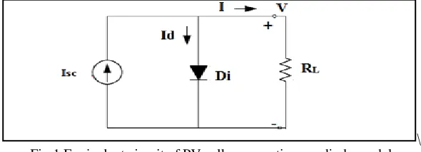
\ Fig:1 Equivalent circuit of PV cell representingone diode model
Fig. 1 shows the one diode model in which an ideal current source is represented along with the parallel diode (this diode represent the output voltage polarity of a PV cell). There are two main parameters of PV cell i.e. open circuit voltage (VOC) and short circuit current (ISC). Under short circuit condition RL=0 hence the short circuit current equals
the total current I (ISC=I). On the other hand under open circuit condition RL=∞ hence the current bypasses through the
intrinsic diode (Di) therefore by using Kirchhoff’s current law (KCL)
ISC= I + Id
i.e. I = ISC-Id
Where, Id is diode current given by the schokely diode equation as follows.
𝐼𝑑 = 𝐼𝑠(𝑒
𝑞𝑉
𝑛
𝑖𝑑𝑒𝑎𝑙
𝑘𝑇
− 1)
Where, Isis reverse saturation current of diode (A), q is electron charge (1.602×10⁻¹⁹C),
V is the volt across diode or PV cell (V), k is Boltzmann’s constant (1.381×10⁻²³
J/K), T is junction temperature in kelvin (k). nideal is the diode ideality factor.
As the one diode model including losses is sufficient to represent the characteristics of PV cell but it does not consider recombination in the PV cell. Hence one extra diode is added in to the above one diode model which gives non ohmic current path in parallel with intrinsic PV cell.
III. MAXIMUM POWER POINT TRACKING
There are several types of direct technique algorithms such as follows:
1. Perturb and Observe method (P&O).
2. Incremental conductance method(IC).
3. Parasitic capacitances.
4. Voltage control maximum power point tracker.
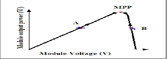
Out of which P & O method is simple and easy to apply hence here this method is used. This algorithm uses a simple feedback loop and some measured parameter. In this method a periodically module voltage is perturb and the corresponding power is compared with that at previous perturb cycle. In this algorithm some perturb is introduced in the system. Because of which there are various power levels of the module. As the power increases the perturbation continuous in the same direction and if power decreases then the same perturbation continues in the opposite direction as shown in fig 2. As the steady state condition occur the maximum power point oscillate along the maximum point therefor the value of perturbation should be as small as possible.
Fig. 2: Graph of power v/s voltage of P & O method.
IV. DIFFERENT CONVERTER MPPT TOPOLOGY
Maximum power point converter is nothing but the dc to dc converter which helps for getting maximum output from the solar cell irrespective of the solar irradiation and temperature condition using the appropriate algorithm. There are various types of converter such as buck converter boost converter and buck-boost converter. This converter is inserted between the solar cell and its load. Since there are various types of dc to dc converter hence it is quite difficult to understand which converter is suitable. Hence there should be an appropriate method which going to deal with these issues. The dc to dc converters are mostly work near about 100% efficiency and many designers have succeeded to get near about this efficiency.
A basic dc to dc converter is known as buck converter whose circuit diagram is shown in fig 3 which employs of a dc input voltage (Vg), switch network which is a single pole double through (SPDT) switch, low pass filter and a load resistor (R). When the switch is connected to position1 then the switch voltage (Vs) is equal to the DC input voltage (Vg) and when the switch is connected to position 2 then switch voltage (Vs) is zero. Here the SPDT switch can be realized by using power semiconductor devices such as MOSFET, IGBT, and BJT etc.
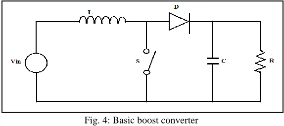
Fig. 4: Basic boost converter
Above boost converter is an alternative way for the buck converter. Boost converter is required to step up the input voltage to the desired output voltage with the help of a transformer action. It is consist of an inductor L, diode D, capacitor C, resistor R, switch S and input voltage V. All these components in the co-ordinated manner supply power to the load in a greater magnitude than in input. The control action of the boost converter is depending upon the switching frequency of the switch (S). The operation of boost converter is depending upon charging and discharging of the capacitor C shown in the above fig. When switch S is open then inductor L starts charging the capacitor through diode D, as soon as switch S is closed charged capacitor starts discharging through load resistor R.
Fig. 5: Buck-Boost Converter.
A Buck-Boost converter is a dc to dc converter which can step up and step down the output voltage with respect to its input voltage. The buck-boost converter is a combination of buck converter and boost converter in the cascaded form. The output of this converter is also the depend upon the switching frequency along with the product of both buck and boost converter duty cycles. The main advantage of buck-boost converter is that it has wide range of output voltage from maximum to almost zero. In the inverting topology the output of this converter is exactly opposite to the input one. Along with all the advantages of the buck-boost converter it has a major drawback that there is no neutral connection in the circuit because of which there is no isolation between input and output supply
.
1. When switch is on (closed) inductor L directly connected to the supply and hence energy stats accumulating in the inductor. At the same time charged capacitor starts supplying to the load.
2. When switch is off (open) then charged inductor L gets connected to the capacitor C and starts supplying to the load.
Fig. 6: Basic Circuit diagram of Cuk Converter.
Many years ago Dr. Cuk has invented the integrated magnetic circuit called DC transformer, where the fluxes created by inductor L1 winding which is connected to the input side is equal and opposite to the fluxes created by the inductor L2 winding as shown in fig 6. Hence DC fluxes are opposite to each other and thus results in mutual cancellation of the DC fluxes. Cuk converter is having more advantages over the buck-boot converter. The main advantages of Cuk converter are that it provides the capacitive isolation between the input and output in the circuit which was not there in the case of buck-boost converter
.
The operation of the Cuk converter is dividing into two modes.
Mode1. When switch is off (open) the stored energy in the inductor L1 is connected to the load through the capacitor C1. Capacitor C1 plays a very important role in transferring the energy from inductor L1 to load.
Mode2. When switch S is turned ON (closed) then current through inductor L1 is rises at the same time capacitor C1 reverse biased diode D hence make it off therefore now capacitor C1 discharges through capacitor C2, inductor L2, and through load resistor R.
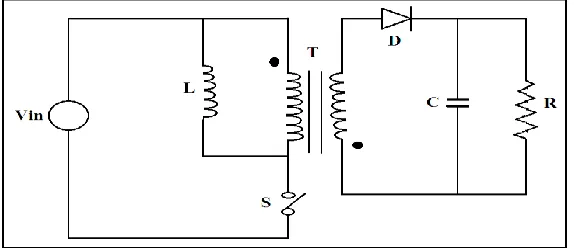
Fig. 7 shows the basic circuit of fly-back converter which is derived from boost converter. The basic operation of fly-back converter is dividing into two modes.
Mode1: when switch S is closed (ON) the primary winding (dot) get connected across the input supply due to which current in the primary winding starts increasing linearly. Due to which primary fluxes starts developing. On the other hand diode is connected to the secondary winding (un-dotted) of the transformer hence it gets reverse biased which tends to block the current flowing in the secondary winding.
Mode2: when switch S is open (off) after being closed for some time then due to the nature of the inductor it reverses its polarity at the same time primary current which were flowing through the primary winding interrupted because of which the diode D which was in the reverse biased earlier becomes forward biased and starts conducting.
V. DIFFERENCE BETWEEN CONVERTER TOPOLOGY
VI. COMPARISON BETWEEN VARIOUS DC TO DC CONVERTERS
The below given table shows the comparison between various dc to dc converters:
Table1:Comparison between various dc to dc converters:
S.N Buck Boost Buck-Boost Cuk Fly-back Forward
1.
Source current waveform is same
as buck-boost
Source current is approximately
smooth
Source current waveform is same as buck
Source current is smooth Source current is smooth Source current is smooth 2.
Because of more stresses on the
input side
No such case More stresses on the source side
No such
case No such case No such case
3. Efficiency is more Less compare to buck
Less compare to buck but more
than boost Less compare to buck but more than boost and buck-boost - -
4. Less voltage ripple
at output More More Less Less Less
5.
Same reference between input and
output
Same Same Same Different Different
6. Single output Single Single Single Multiple Multiple
VII. CONCLUSION
.
When the external environment changes suddenly the system cannot track the maximum power point quickly. With the use of different types of dc to dc converter it is possible to track the maximum power point (MPP) with increase in efficiency of the system, but on the other hand with the excess use of dc to dc converter there can be decrease in overall efficiency of the system. Hence there will be an approach where with the help of detail study of the comparison of dc to dc buck and buck-boost converter topologies, to suggest an appropriate converter.
REFERENCES
[1] V. Di Dio, D. La Cascia, R. Miceli Member IEEE, C Rando. “A Mathematical Model toDetermine the Electrical Energy Production in Photovoltaic Fields underMismatchEffect”. Clean Electrical Power, 2009 International Conference on9-11 June 2009 46 – 51.
[2] V. Di Dio, D. La Cascia, R. Miceli Member IEEE, C Rando. “A Mathematical Model toDetermine the Electrical Energy Production in Photovoltaic Fields underMismatchEffect”. Clean Electrical Power, 2009 International Conference on9-11 June 2009 46 – 51.
[3] Gregor Simeonov. “Resonant Boost Converter for Distributed Maximum Power Point Tracking in Grid-Connected Photovoltaic Systems”. Graduate Department of Electrical and Computer Engineering University of Toronto, 2010, page(s) 13-24.
[5] Trishan. Esram. Student Member, IEEE, and Patrick L. Chapman, Senior Member, IEEE “Comparison of Photovoltaic Array Maximum Power Point Tracking Techniques”. Energy Conversion,IEEE TransactionsonVolume: 22, DOI:10.1109/TEC.2006.874230Publication Year: 2007, Page(s): 439 – 449.
[6] A. Luque, S. Hegedus, “Handbook of photovoltaic science and engineering”, John Wiley & Sons, Singapore, 2003.
[7] A. Gow and C.D. Manning, “Development of a photovoltaic array model for use in Power electronics simulation studies”, IEE Proc. Electr. Power Appls.vol. 146, no.2, Pp.193-200, Mar. 1999.
[8] Hairul Nissah Zainudin Saad Mekhilef Department of Electrical Engineering University of MalayaKuala Lumpur, Malaysia. “Comparison Study of MaximumPower Point Tracker Techniques for PV Systems “.Proceedings of the 14t International Middle East PowerSystems Conference (MEPCON’10), Cairo University, Egypt, December 19-21, 2010, Paper ID 278.
[9] Saurav Satpathy 108EE074. “Photovoltaic power control using Mppt and boost Converter”. A thesis submitted in Partial fulfillment of the requirements for the Degree of Bachelor of Technology in Electrical Engineering by
[10] Dr. B.J. Ranganath Dean academic EIT, Ummathoor, Mysore, India Mr. Amurth R.T Research Scholar JJTU, Jhunjhunu -333001, Mysore India. “Design of DC/DC Buck- Boost Converter Charge Controller For Solar Power Applications”.
[11] Robert W. Erickson. “DC-DC Power Converters”. Department of Electrical and Computer Engineering University of Colorado Boulder, CO 80309-0425. Aerospace and Electronic Systems, IEEE Transactions on Volume: AES- 21, DOI:10.1109/TAES.1985.310664 Publication Year: 1985 , Page(s): 791 - 799 Cited By: Papers (42)
[12] Srushti R.Chafle, Uttam B. Vaidya Z.J.Khan “Design of cuk converter with Mppt Technique”. M-Tech Student, RCERT, Chandrapur, India Professor, Dept. of Electrical & Power, RCERT, Chandrapur, India HOD & Professor, Dept. of Electrical & Power, RCERT, Chandrapur, India. International journal of innovative Research in electrical, electronics, Instrumentation and control engineering Vol. 1, issue 4, July 2013.