SCDBI
Encoding Scheme for NoC Links
N. Rajesh
Master of Technology,Department of ECE, Vardhaman College of
Engineering,
B.V.S.L.Bharathi
Assistant professor, Department of ECE, Vardhaman College of
Engineering,
M.Venkata Theertha
Master of Technology,
Department of ECE, Vardhaman College of
Engineering,
ABSTRACT
As the technology shrinks, the power consumed by links dominating the power consumed by routers. We can reduce power consumed by links by using clock gating and data encoding schemes. Clock gating is one method to reduce switching power in NoC links and we can provide this at the time of synthesis by using EDA tools. The data encoding scheme exploits the wormhole switching techniques and works on an end-to-end basis. That is, flits are encoded by the network interface (NI) before they are injected in the network and are decoded by the destination NI. This makes the scheme transparent to the underlying network since the encoder and decoder logic is integrated in the NI and no modification of the routers architecture is required Data encoding schemes are other techniques to reduce switching power in NoC links by reducing self transition and coupling transition in links. In t his paper, we proposed data encoding scheme called self and coupling driven bus invert (SCDBI). By using this method we can reduce the switching power by 34.64% without any significant degradation in area and performance.
Keywords
Synthesis, Coupling capacitance, self capacitance, data encoding, low power, network on chip (NoC), power analysis.
1.
INTRODUCTION
As the number of IP cores integrated into a system on-chip (SoC) increases, the role of the interconnection system becomes more and more important because these are the limiting factors for performance and power consumption in current and next generation SoCs [2].In ultra deep submicron silicon design is mainly dominated by interconnection issues. As the number of cores increases, the total length of the interconnection wires increases, resulting in long transmission delay, larger area and higher power consumption. Another problem is, the length of wires decreases with technology, in turn, it will increase coupling capacitance, and the height of the wire material increases resulting in greater fringe capacitance [3]. In the multi core era, as the number of cores increases significantly on SoC, the communication systems also need to change to support the multi core communication demands. NoC is the solution to scalability issues of future many-cores systems and to achieve the performance, reliability, and power requirements.
The importance of interconnects in complex many -core chips has outrun the importance of transistors as a dominant factor of performance, power, cost, and reliability [6], [7]. There are few other types of interconnect architectures like simple bus architecture, point to point architecture and segmented bus architecture etc. but NoC can only address the global interconnect problems (like delay, power, noise, scalability, reliability), system integration and productivity problem (i.e. long designing problem), and emergence of chip multiprocessors. NoC-based interconnect is formed by three basic elements those are network interfaces (NIs), routers, and links. As technology moves down, the power dissipated by the routers and NIs is dominated by links. In this paper we have focused on power dissipated by network links. The power dissipation in links is due to switching activity (both self and coupling) induced by subsequent data pattern traversing the link [1]. Data encoding schemes are the best way to reduce power dissipated by the network links by reducing the switching activity in links. The basic idea is to encode the data before traversing through links to reduce the switching activity of the links [1]. In this proposal, the data is encoded before transmission and is decoded at the destination. It is transparent approach with respect to the NoC fabric as it does not require modifications to router.
This proposal will reduces the power with the expense of overhead (both in terms of power dissipation and silicon area) due to the encoding and decoding logic integrated into the NI. The rest of this paper is organized as follows. An overview of the proposed data encoding scheme is presented in Section 2. In Section 3, we perform a general quantitative analysis. The proposed data encoding scheme i.e. SCDBI along with a possible hardware implementation and its analysis is presented in detail in Section 4. Synthesis and simulation have shown in Section 5. Finally, in Section 6&7 we draw our conclusion and discuss possible future developments.
2.
OVERVIEW OF THE PROPOSAL
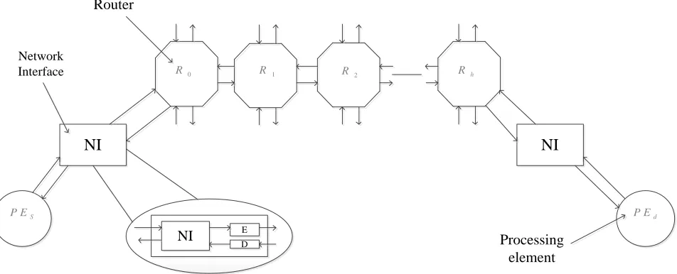
NI
NI
0R R 1 R 2 R h
S
P E P Ed
NI
ED Network
Interface
Router
[image:2.596.63.539.76.269.2]Processing
element
Figure 1.
General sche me of the pr oposed appr oac h.As shown in Fig. 1, the NI is integrated with an encoder (E) and a decoder (D) block. Encoder encodes all the outgoing flits of the packets except header flit to minimize the power dissipated by links in which the packet is traversed. The header flit contains control information (destination address, packet size, and so on) so no need to encode. Header flit should be processed by the routers through the routing path. In the same way, the incoming flits in the NI (with the exception of the header flit) should be decoded by the decoder block.
3.
GENERAL QUANTITATIVE
ANALYSIS
In this section, the general model to quantify the power saving is defined using an end-to-end data encoding technique as sketched in Fig. 1.Then, impacts of several architectural and communication-related parameters on power saving will be analyzed .
Let us consider a packet of n + 1 flits
{ , 1, 2, ..., }
pkt bH b b bn
(1)
Where,
b
H is the header flit and b ii, 1, 2, 3....n are the body flits.Let us consider that a packet is transmitted from source
processing element (PEs) to destination processing element
(PEd) involving h hops (see Fig.1). And that packet will hop through h links and will be processed by h + 1 routers (from
0 R
toRh). The power dissipated to transmit the packet can be expressed as
( ) ( )
( ) 2( 1) ( 1) H ( 1) B ( 1)
p pkt n pNI h pR h npR h n pL
(2)
Where
(H)
R
p
and
( )B R
p
the power dissipated by the router
when header flit and the body flit, respectively and pNI is power dissipated by the network interface and
p
Lis power dissipated by alink to transmit a flit. Now, let us take the case in which the NI encodes body flits of the packet before traversing through links and decodes each received body flit at another end of link. In this case, the power dissipated to transmit the packet can be expressed as
( ) ( )
( ) 2 2 ( 1) H ( 1) B ( 1)
p pkt pNI n pNI h pR h npR h n pL
(3)
Where, p NI
is the power dissipated by the NI integrated with
the encoder and decoder logic andp L
is the power dissipated to transmit an encoded flit over a link. Let us indicate with
pED the power contribution of the encoding/decoding logic.
We can approximate
p
NI as the pNI plus the overhead due to the encoding/decoding logic
pNI pNI pED
(4)
Substituting (4) in (3) we have
( ) ( ) ( ) 2 2 ( ) ( 1) H ( 1) B ( 1)
p pkt pNI n pNI pED h pR h npR n h p L
(5)
1 ( ) / ( )
PR P pkt P pkt
(6)
4.
PROPOSED ENCODING SCHEMES
In this section, we present self and Coupling Driven Bus Invert (SCDBI) encoding scheme. Its goal is to reduce the power dissipation in NoC links by reducing switching activity. First, we will briefly analyze the different factors involving in determining the power dissipated by a link.
4.1
Powe r ModelThe dynamic power (short circuit+ switching power) consumed by the interconnects and drivers is given by
2
[ 0 1( ) ]
p T cs c T cc c v F
l dd ck
(7)
Where vddis the supply voltage, Fck is the clock frequency, cs is the self capacitance (which includes the parallel-plate
capacitance and the fringe capacitance), cl is the load capacitance, and cc is the coupling capacitance. 0 1T is the average number of effective transitions per cycle for cs and Tc is the average number of effective transitions per cycle for cc .We can compute 0 1T
by counting the number of 01 transitions in the links in two consecutive
transmissions and Tc is by counting the correlated switching among physically adjacent bus lines. Precisely, we can differentiate four types of coupling transitions as follow. If one line toggles while other stays unchanged then it is a Type I transition. If one line switches from low to high while the other switches from high to low a Type II transition will occur. A Type III transition occurs when both lines switch simultaneously. Finally, if both lines do not switch i.e. they will be in a same state then it is said to be Type IV transition is occurred. The effective switched capacitance is different for different transition types. So, the coupling transition activity
Tc is a weighted sum of the different type of coupling
transition contributions. We can express Tc as 1 1 2 2 3 3 4 4
Tc k T k T k T k T
(8)
According to [2], 1k = 1, 2k = 2, and 3k = 4k = 0 and here, 1
k
is considered as reference for other types of transition. The
effective capacitance in Type II transition is twice the effective capacitance of Type I transition. We know that in Type III transition both signals will switched simultaneously,
cc is not charged (here we consider that there is no misalignment between the two transitions). Finally, in Type
IV transition there is no dynamic charge distribution overcc. Based on this, (7) can be expressed as follow:
2 [0 1( ) (1 2 2) ] p T cs cl T T cc vdd ckF
(9)
In the next subsection, we present SCDBI encoding scheme, its goal is to minimize transitions to minimize the switching activity.
4.2
SCDBI
Looking at (7) and (8) we have
[ 0 1 (1 1 2 2 3 3 4 4) ] p Tcs k T k T k T k T cc
(10)
The link power consumption if the data is inverted,
' ' ' ' ' ' ' ' '
[0 1 (1 1 2 2 3 3 4 4) ] p Tcs k T k T k T k T cc
(11)
Where, ' 0 1 T
, ' 1 T
, ' 2 T
, ' 3 T
and ' 4 T
are the self transition activity and the coupling transition activities of Types I, II, III, and IV, respectively, if the data is inverted before being transmitted. We need to determine the relationship between the coupling transition activities if the flit is transmitted as is and with its bits inverted. Table I reports for each transition type and how it mutates if the flit is inverted. Data are organized as shown in table I. We can observe from Table I that Type I transitions will remain as Type I transitions even if the flit is inverted and Type II and Type III transitions will changed to Type IV transitions if the flit is inverted. Type IV transitions will mutates either in Type II or Type III
transitions. In particular, transitions indicated as * 4 T
in the table mutate in Type III transitions whereas that indicated
with ** 4 T
mutate in Type II transitions. In the same way, it is
simple to find that ' 0 1 T
= 0T0. We can express (12) as a function of 1T , 2T , 3T ,
* 4 T
and ** 4 T
as
' ' ** *
[0 0 ( 1 1 2 4 3 4 4( 2 3)) ] p T cs k T k T k T k T T cc
(12)
If '
p p , then invert the data flits. Taking (10) and (12) and according [2] k11,k2 2, k3k4 0 and cc/cs 4, we obtain the following invert condition:
**
8 8
0 1 2 0 0 4
T T T T
(13)
In conclusion, the SCDBI encoding scheme simply inverts the flit before its transmission if and only if the invert condition (13) is satisfied.
[image:3.596.311.543.390.607.2]
Table 1 How Transitions Mutate If Data Is Inverted
Time
Normal
Inverted
1
t
t
Type I
00 00 11 11
01 10 01 10
Type I
00 00 11 11
10 01 10 01
1
t
t
Type II
01 10
10 01
Type IV
01 10
01 10
1
t
t
Type III
00
11
11
00
Type IV
00 11
00 11
1
t
t
Type IV
00 11 01 10
00 11 01 10
T
4**T
4*Type II and III
00 11 01 10
11 00 10 01
T
3T
2Do not invert
invert
invert
Y
Y
Y
N
N
N
**
2 4
T
T
* *
2 4
T T
0 1 0 0
T T
Figure 2. Flowchart to evaluate the invert condition (13)
Consider w bits of the incoming body flits are indicated
with
x
i, i0,1, 2, ...w1 whereas the previously encodedhas to be inverted (inv = 1) or left as is (inv = 0) at decoder side. The first level of the encoder determines the transition
type. The four input blocks 2T and ** 4 T
assert their output if
1 1
y yi i x xi i
is a 2T or a ** 4 T
transition, respectively.
The two input blocks 0 1T and 0T0 assert their output if yixi
is a 0 1T or a 0T0transition, respectively. Ones counters and comparators are required to design SCDBI encoder. This encoder designed by using equation (13) and from figure2 [1].
5.
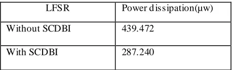
SYNTHESIS REPORT
[image:5.596.53.282.374.443.2]The encoder and the decoder had been designed in Verilog HDL described at the RTL level, synthesized with cadence RTL Compiler and mapped onto TSM C 45 nm technology library. We have calculated the power consumed by Linear Feedback Shift Register (LFSR) with and without using SCDBI and those results are shown in table II. The power saved by SCDBI is 34.64%. The impact on area is very less and it is approximately 8%. The data is inverted whenever SCDBI finds self transitions and coupling transitions in NoC links and we can observe that in table 2.
Table 2
Power dissipation without SCDBI and with SCDBI
LFSR Power d issipation(µw)
Without SCDBI 439.472
With SCDBI 287.240
6.
CONCLUSION
The power dissipated by the links of a NoC contribute significant fraction of the total power budget [5]–[7]. In this paper, we have proposed the use of data encoding techniques as a viable way to reduce power dissipation in NoC links. The SCDBI sc heme is transparent because they operate on an end-to-end basis and no need to modify the router architecture, only the NI is to be augmented with the encoder and decoder. Although, it represents an overhead, does not introduce a significant penalty both in terms of cost (i.e., silicon area) and latency. The simulation results and synthesis results have shown that, by using the SCDBI encoding scheme it is possible to reduce the power contribution of both the self switching activity and the coupling switching activity in inter-routers links. Precisely, as compared to a baseline implementation in which no data encoding techniques are used, a reduction of up to 34.64% of power dissipation has been observed without any significant degradation in terms of both performance and silicon area.
7.
FUTURE SCOPE
Network on Chip (NoC) is an emerging model to provide communication on M ulti Processor System on Chip (MPSoC-contains multiple processors on a single chip). So the power consumption is more. By integrating encoding logic to Network Interface (NI-one part of NoC) power can be decreased significantly without any significant overhead area and overhead. Already, we have Bus Invert (BI), Coupling Driven Bus Invert (CDBI) and other encoding schemes but BI reduces the power dissipation of links only if self transitions exist and for CDBI, if coupling transitions exist so the power saving is less than power saving by using SCDBI.
8.
REFERENCES
[1] M aurizio Palesi, Member, IEEE, Giuseppe Ascia, Fabrizio Fazzino, Member, IEEE, and Vincenzo Catania “Data Encoding Schemes in Networks on Chip” IEEE Transactions On Computer-Aided Design Of Integrated Circuits And Systems, vol. 30, no. 5, may 2011pg.no.774-786
[2] K. W. Kim, K. H. Baek, N. Shanbhag, C. L. Liu, and S. M. Kang, “Coupling-driven signal encoding scheme for low-power interface design,” in Proc. IEEE/ACM Int. Conf. Comput.-Aided Design, Nov. 2000, pp. 318–321. [3] M. R. Stan and W. P. Burleson, “Bus invert coding for
low power I/O,” IEEE Trans. Very Large Scale Integr. Syst., vol. 3, no. 1, pp. 49–58, M ar. 1995.
[4] H.-J. Yoo, K. Lee, and J. K. Kim, Low-Power NoC for High-Performance SoC Design. Boca Raton, FL: CRC Press, 2008.
[5] G. D. M icheli and L. Benini, Networks on Chips: Technology and Tools.San M ateo, CA: M organ Kaufmann, 2006.
[6] L. Benini and G. D. Micheli, “Networks on chips: A new SoC paradigm,” IEEE Comput., vol. 35, no. 1, pp. 70–78, Jan. 2002.
[7] J. Henkel, H. Lekatsas, and V. Jakkula, “Encoding schemes for address busses in energy efficient SoC design,” in Proc. 11th VLSI-SoC Int. Conf. Very Large Scale Integration, Dec. 2001, pp. 744–749.
[8] M. Palesi, F. Fazzino, G. Ascia, and V. Catania, “Data encoding for low power in wormhole-switched networks-on-chip,” in Proc. EuromicroConf. Digital Syst. Des., 2009, pp. 119–126.