http://dx.doi.org/10.4236/jsip.2015.63022
Implementation of High Performance
Electronic Circuits for Zero Suppression and
Encoding of Digital Signals
Ashraf H. Yahia
1, Amr Radi
1, Salwa M. Youssef
21Physics Department, Faculty of Science, Ain Shams University, Cairo, Egypt 2Higher Technological Institute, 10th of Ramadan City, Egypt
Email: [email protected], [email protected]
Received 18 June 2015; accepted 22 August 2015; published 25 August 2015
Copyright © 2015 by authors and Scientific Research Publishing Inc.
This work is licensed under the Creative Commons Attribution International License (CC BY).
http://creativecommons.org/licenses/by/4.0/
Abstract
This paper presents a design of a data processing circuit for receiving digital signals from front end-electronic board chips of a specific nuclear detector, encoding and triggering them via specific optical links operating at a specific frequency. Such processed signals are then fed to a data acqui-sition system (DAQ) for analysis. Very high-speed integrated circuit hardware description lan-guage (VHDL) algorithms and codes were created to implement this design using field program-mable gate array (FPGA) devices. The obtained data were simulated using international standard simulators.
Keywords
DAQ, FPGA, VHDL, ASICs, ISE, ISim
1. Introduction
Field programmable gate array (FPGA) is a chip designed to be programmed and reprogrammed by customers after manufacturing. Customized designs can be made after the chip fabrication. FPGAs are considered to be the most powerful programmable logic devices today [1].
asso-ciated with ASICs at cost of 5 to 25 times area, delay and performance.
While software provides the flexibility to execute a large number of tasks, typically its performance when run on a sequential processor is orders of magnitude slower than ASICs and FPGAs. These two factors make FPGAs an attractive middle ground for applications that require performance that cannot be achieved by soft-ware running on sequential processors; but yet require a degree of flexibility not possible with ASICs imple-mentation. Traditionally, FPGAs have been used for applications that process large streams of data, where processes can be executed in parallel and independent of each other. In fact, FPGAs can achieve several orders of magnitude faster speeds compared to microprocessors by exploiting the parallelism in applications [2] [3].
Since many applications such as signal processing [4], network communications [5], video communications [6] [7], cryptographic applications [8], neural networks [9]-[11], genetic algorithms [12]-[14] and other specific computations have inherent parallelism profiles that are easily exploitable; they can be implemented using FPGA in a relatively easy way to accelerate their computation.
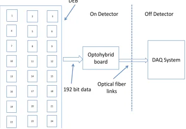
In this paper, we have written an algorithm to be implemented on an FPGA system for processing the data to be conveyed to the DAQ. The detector system consists of a nuclear detector, a readout system and a DAQ as shown in Figure 1. Moreover, the block diagram that describe the readout system components of the detector.
The detector converts the energy deposited/induced by a particle (or photon) to an electrical signal. This ana-log signal is fed to the readout board, which basically contains front-end electronic board chips. A chip has two main functions: the first function is the triggering which provides programmable “fast OR” information based on the region of the sensor hit; the second function is the tracking, which provides precise spatial hit information for a given triggered event. Thus the digital data leaves the chip in parallel.
There are several goals for this study: First, Collecting the digital data from the front-end electronic board chips. Second, removing the redundant zeros from the digital data, which will be referred to as Zero Suppression (ZS) and indicating which chip has hit. Finally, processing those signals to handle specific type of optical fiber is to be able to trigger them to the DAQ system. Our algorithm/code is written in Verilog and VHDL as hardware description language and implemented on Xilinx Spartan 6 board. FPGA Spartan 6 family is described in [15].
2. Data Processing System Design
[image:2.595.125.504.443.705.2]The block diagram shown in Figure 1 illustrates the main system components for the readout of the detector
Figure 1. Block diagram of the main design system components. 1
4
7
10
13
16
19
22
5 2
8
11
14
17
20
23
3
9
12 6
15
18
21
24
Optohybrid
board
DAQ System
Off Detector
On Detector
Optical fiber
links
192 bit data
system and is divided into two main parts; namely On-Detector and Off-Detector. Visible in the On-Detector part is the division of the detector into 24 sectors. The 128 strips from each sector are connected to the inputs of the front-end chip via a connector on a board known as the detector readout board. The chip itself is mounted on a hybrid, which plugs into the readout board connector. The control, readout and power to/from the chip hybrid is delivered via electrical signals running through a large flat pcb known as the Detector Electronic Board (DEB). An opto-hybrid board also plugs into the DEB, an FPGA as well as optical receivers and transmitters to provide the link to the Off-Detector region.
The above figure shows the process of collecting the output digital signals data from the front-end electronic boards, reducing data size, identifying which chip has hit and changing data size to adapt the chosen optical fi-ber.
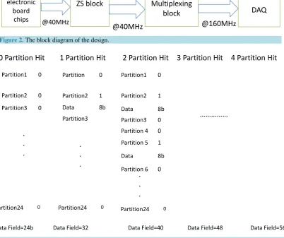
It is clear that the top-down design, which is written in VHDL and Verilog mainly, consists of data processing module, Zero Suppression component and multiplexing component.
2.1. Zero Suppression (ZS) Component
In this component, the size of the data packet is a function of the number of hits in the chip. This enables very small data packets and hence the highest possible data transmission rate. This is very reasonable for operation at high trigger rates. The disadvantage is that for high occupancy some losses could be incurred.
[image:3.595.113.518.344.713.2]The principle is as follows: The 192 channels, Figure 2, are divided up into 24 partitions. Each partition con-tains 8 channels. For each event only the partitions containing data will be transmitted. The sequence for gene-rating the zero suppression data field is shown Figure 3. The packet has already identified how many partitions
Figure 2. The block diagram of the design.
Figure 3. Zero suppression data field.
ZS block
Multiplexing
block
64b
192b in
Parallel
DAQ
16b
@160MHz
@40MHz
@40MHz Front-end electronic board chips0 Partition Hit
1 Partition Hit
2 Partition Hit 3 Partition Hit 4 Partition Hit
Data Field=24b Data Field=32 Data Field=40 Partition1 0
Partition2 0 Partition3 0 Partition 0 Partition2 1 Data 8b Partition3 Partition1 0
Partition2 1
Data 8b
Partition3 0 Partition 4 0 Partition 5 1
Data 8b
Partition 6 0
.
.
.
Partition24 0 Partition24 0.
.
.
Partition24 0.
.
.
[image:3.595.114.517.373.710.2]are contained within the data field. Then, a sequence of partition bits arrives to identify which partition contains data.
A “0” means empty partition and a “1” means partition containing hits. The sequence is in order, hence the first bit represents partition one containing channels 1 - 8, the second bit represents partition 2 containing chan-nels 9 - 16 etc.
If a “1” is detected in the sequence then the following 8 bits represent the 8 channels within that partition. Hence the example with 2 partitions hit shows hits within partitions 4 and 6. Once all the partitions have been read the sequence stops.
2.2. Multiplexing Component
This component gets the 64 bits of data at 40 MHz clock cycle from the ZS component and multiplexes them to 16 bits at 160 MHz, Figure 2. So the data at that time is ready to be triggered via the optical links, which are connected to the DAQ system as shown in Figure 1. All the design has been implemented on the Spartan6 board [15], which is embedded in the opto-hyprid.
The opto-hybrid consists of mezzanine board mounted along the DEB board. The tasks of the opto-hybrid board are to synchronize the data sent by the front-end electronic chips, zero-suppress the trigger data, code them and send them via optical links to the triggering electronics.
3. Verification and Results
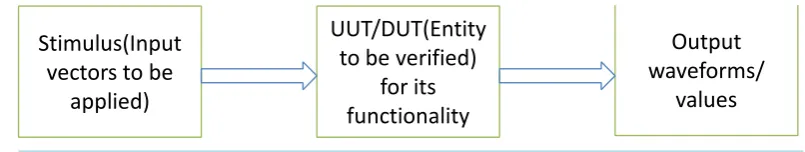
Verification of the circuit functionality is usually done as the first step once completing VHDL code. Verifica-tion of design without actual hardware in place is done using simulaVerifica-tion. For simulating any design two things are required; that is, design to be tested and stimulus to inputs. Two approaches are used in VHDL for simula-tion: one is assigning input values in simulation window and getting the output waveforms and the other is using testbenches.
In this work testbench has been used. Testbench is different from VHDL simulation of the circuit which uses run-time assignment of input values. The purpose of a testbench is to verify the functionality of a developed model or package. Figure 4 shows a typical testbench structure [16].
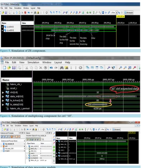
That has been done using ISim simulator that let’s you perform functional (behavioral) and timing simulations for VHDL, Verilog, and mixed-language designs. So for the first component, that is the ZS, the simulation re-sults are shown in Figure 5 as has been expected. As an example, consider the case of three chips under hit; the output result is found to be 24 bits for the 24 chips on the DEB followed by 8 bits of data (for each chip). So in our example, the output will be 24 + 8 + 8 + 8 = 48 bits. To output 64 bits, the rest will be filled with 16 bits as filler. This is in consistence of the results that has been taken from the simulator.
For the second component, that is the Multiplexing component which takes its input data from the ZS at a rate of 40 MHz/25ns clock cycle, the output depends on the control signal (ctrl). Four control signals have been used. The first ctrl signal of “00” gives the first 16 bits of the data string, the same output happens for the second, third and fourth ctrl signals; i.e. “01”, “10” and “11”. Figure 6 shows the simulation of this component in case of “10” ctrl. As one notices, the result of the simulation is as had been expected (encircled in the figure).
[image:4.595.109.512.634.710.2]For the whole system design (including both previously mentioned components); to simulate the circuit it should take 192 bits of input data for an output of 16 bits (each of which is 160 MHz/6.25ns clock cycle). This matches with the optical fiber characteristics (which connects the opto-hybrid board and the DAQ system, shown in Fig-ure 1). Figure 7 shows the simulation results of the whole module, named as data processing module. This fig-ure shows the results of the case where three chips had hit as had been expected. The given simu lated results were a direct product of the use of ISE program and ISim simulator [17] together with the available input data.
Figure 4.Typical test bench.
Stimulus(Input
vectors to be
applied)
UUT/DUT(Entity
to be verified)
for its
functionality
Output
waveforms/
Figure 5.Simulation of ZS component.
[image:5.595.88.540.78.617.2]Figure 6. Simulation of multiplexing component for ctrl “10”.
Figure 7.Simulation of data processing module.
4. Conclusion
5. Future Work
We will use new algorithm that allows raising the number of chip hits which could be recognized. In addition, we will use new versions of FPGA chips to improve the performance of the design.
References
[1] Nie, C.L. (2012) An FPGA-Based Smart Database Storage Engine. Eidgenössische Technische Hochschule Zürich, Department of Computer Science, Systems Group.
[2] Hauck, S. and Dehon, A. (2008) Reconfigurable Computing. Morgan Kaufmann, United State.
[3] Xu, J. (2009) A FPGA Hardware Solution for Accelerating Tomographic Reconstruction. MSc Thesis, University of USA, New York, 17-18.
[4] Vetterli, M., Kovačević, J. and Goyal, V.K. (2014) Foundations of Signal Processing. Cambridge University Press, Cambridge.
[5] Cheung, O. and Leong, P. (2002) Implementation of an FPGA Based Accelerator for Virtual Private Networks. IEEE
International Conference on Field Programmable Technology (FPT), Hong Kong, 16-18 December 2002, 34-43.
http://dx.doi.org/10.1109/fpt.2002.1188662
[6] Gause, J., Cheung, P. and Luk, W. (2000) Static and Dynamic Reconfigurable Designs for a 2D Shape-Adaptive DCT. In: Hartenstein, R. and Grüunbacher, H., Eds., Field-Programmable Logic and Applications, FPL, Springer-Verlag, New York, 96-105. http://dx.doi.org/10.1007/3-540-44614-1_11
[7] Villasenor, J., Jones, C. and Schoner, B. (1995) Video Communications Using Rapidly Reconfigurable Hardware.
IEEE Transactions on Circuits and Systems for Video Technology, 5, 565-567.
[8] Hämäläinen, A., Tommiska, M. and Skyttä, J. (2002) 6.78 Gigabits per Second Implementation of the IDEA Crypto-graphic Algorithm. In: Glesner M., Zipf, P. and Renovell, M., Eds., Field Programmable Logic and Applications.
Reconfigurable Computing Is Going Mainstream, LNCS 2438, Springer-Verlag, New York, 760-769.
http://dx.doi.org/10.1007/3-540-46117-5_78
[9] Bade, S. and Hutchings, B. (1997) FPGA Based Stochastic Neural Network Implementation. Proceedings of the IEEE
Workshop on FPGAs for Custom Computing Machines, Napa Valley, 10-13 April 1994, 189-198.
http://dx.doi.org/10.1109/FPGA.1994.315612
[10] Lysaght, P., Stockwood, J., Law, J. and Girma, D. (1994) Artificial Neural Network Implementation on a fine-Grained Fpga. Field-Programmable Logic, 849, 421-431.
[11] Gadea, R., Cerd, J., Ballester, F. and Mochol, A. (2000) Artificial Neural Network Implementation on a Single Fpga of a Pipelined On-Line Back Propagation. Proceedings of the 13th Conference on International Symposium on System
Synthesis, Madrid, 20-22 September 2000, 225-230. http://dx.doi.org/10.1109/ISSS.2000.874054
[12] Graham, P. and Nelson, B. (1996) Genetic Algorithms in Software and in Hardware—A Performance Analysis of Workstation and Custom Computing Machine Implementations. Proceedings of the IEEE Symposium on FPGAs for
Custom Computing Machines, Napa Valley ,17-19 April 1996, 216-225. http://dx.doi.org/10.1109/fpga.1996.564847
[13] Bland, I.M. and Megson, G.M. (1998) The Systolic Array Genetic Algorithm, an Example of Systolic Arrays as a Reconfigurable Design Methodology. Proceedings of the IEEE Symposium on FPGAs for Custom Computing
Ma-chines, Napa Valley, 15-17 April 1998, 260-261. http://dx.doi.org/10.1109/fpga.1998.707907
[14] Aporntewan, C. and Chongstitvatana, P. (2001) Hardware Implementation of the Compact Genetic Algorithm.
Pro-ceedings of the 2001 IEEE Congress on Evolutionary Computation, Seoul, 27-30 May 2001, 624-629.
http://dx.doi.org/10.1109/cec.2001.934449
[15] Xilinx (2009) Spartan-6 FPGA Configuration User Guide Xilinx, 2.7. [16] Kau, G. (2011) VHDL: Basics to Programming, 150.