HDLC Implementation in Wireless Sensor Networks
Deepika Sharma
Electronics and Communication Engineering, Lovely Professional
University Punjab, India
Rajeev Kumar Patial
Assistant Professor, Electronics and Communication Engineering, Lovely
Professional University Punjab, India
ABSTRACT
The work aims the designing and implementing an efficient HDLC chip. We use pipelining technique in HDLC register module which increases the throughput of the system and also helps in decreasing the delay of the system. In pipeline technique, number of instructions has been executed at the same time. The HDLC chip designed here supports two way communications means it supports full duplex communications which means that it can transmit and receive continuously. In this paper we adopt Xilinx’s Spartan-3E for HDLC implementation and for hardware simulation we use Modelsim SE 6.2C.
Keywords
Cloud Computing, Billing, SaaS, PaaS, IaaS
1. INTRODUCTION
The WSN change the way by which the people interact with the physical world by using the new technologies. Wireless technologies for telecommunications, are Global System Mobile, Code Division Multiple Access, General Packet Radio Service and Wi-MAX etc. has great impacts on the personal communication[1]. As the complexity of environmental monitoring system e.g. temperature, humidity etc. is increasing, the information gathered by a WSN cannot meet the requirements of the human being’s. In order to achieve these requirements, we introduce image, videos, audio and some other multimedia information to WSN [2].
In daily life PSTN is a commonly used voice communication network and acts as a bridge between telephone user’s and WMSN. To access interface to PSTN, HDLC protocol is used which provide the reliable information during transmissions. HDLC is a bit-oriented protocol. This protocol is defined in data link layer i.e. Layer 2 of OSI model. HDLC is a commonly used layer 2 protocol and was developed by the International Organization for Standardization (ISO). HDLC comes under the ISO standards ISO 3309, ISO 8885 and ISO 4335.
HDLC is a code transparent protocol which means that it can transmit any bit pattern between two flags. HDLC uses a special bit pattern 01111110 (0x7E) as a delimiter or also called as flag. This flag pattern can be found anywhere between two flags. HDLC has many subsets, out of which two are used as a Synchronous Data Link Control and Link Access Procedure- Balanced.
Technically HDLC has following aspects [5]:
1.1
Stations and Configurations
1.2
Operational Modes
1.3
Non-Operational Modes
1.1
Stations and Configurations
HDLC has three types of stations for data link control: 1.1.1
Primary Station
Primary Station acts as master stations which send command frame to secondary station and receive response frame from secondary station. It is responsible for data flow on the link and also takes care of error recovery at data link level.
1.1.2
Secondary Station
Secondary station acts as slave to primary station. It receive command frame from primary station and send response command to primary station. It is controlled by primary station and activated when receive command from primary station.
1.1.3
Combined Station
Combined Station takes care of functionality of primary and secondary station. These stations can communicate with two stations in balance mode and have capabilities of both primary and secondary station. These stations can transmit and receive both command frame and response frame.
Following three configurations are defined by HDLC as:
1.1.4
Unbalanced Configuration
1.1.5
Balanced Configuration
1.1.6
Symmetrical Configuration
1.2
Operational Modes
In HDLC, mode is defined as the relationship between two devices involved in an exchange i.e. the mode describes who controls the link. Exchange of data between two stations using unbalanced configurations are always conducted in normal response mode. Different modes of operations in HDLC are:
1.2.1
Normal Response Mode (NRM)
1.2.2
Asynchronous Response Mode (ARM)
1.2.3
Asynchronous Balanced Mode (ABM)
1.3
Non- Operational Modes
In non-operational mode there are two disconnected mode (NDM and ADM) which is totally different from operational mode. In disconnected mode, the secondary station is logically disconnected not physically from the link. HDLC also defines three non-operational modes as given below:
1.3.1
Normal Disconnected Mode (NDM)
1.3.2
Asynchronous Disconnected Mode (ADM)
1.3.3
Initialization Mode (IM)
proposed architecture and simulations under the environment of Modelsim 6.2C.
2.
ARCHITECTURE OF HDLC
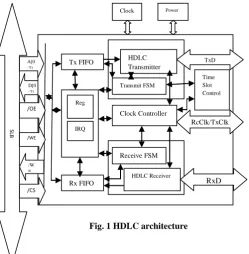
[image:2.595.39.289.185.440.2]The block diagram of HDLC is off-chip modules and on-chip modules. The off-chip modules consist of clock, power and SLB (Simple Local Bus) and on-chip module contain different sub-modules. In this architecture, data transmitted by the CPU is transmitted and received through different sub-modules. The detailed explanation of the architecture is given as below [12]:
Fig. 1 HDLC architecture
Fig. 1 HDLC architecture
2.1
Design of Off-Chip Interface Module
The off-chip modules consist of clock, power and SLB (Simple Local Bus). The interface of Power, Clock and SLB to HDLC chip is explained as:
2.1.1
Interface between CPU and HDLC chip
The CPU and HDLC chip are connected through SLB interface. HDLC’s registers are used by CPU for implementation and data transmission.
2.1.2
Receiving and sending interfaces of HDLC
Data is transmitted between two HDLC chips simply by connecting two chips together. The transmission mode supported by HDLC chips are Bus mode and TDM mode.
2.1.3
HDLC Chip Clock
The clock is generated by crystal oscillator. The transmission and reception of data is done on the basis of the rising and falling edge of the clock. The HDLC chip supports multiple clock modes.
2.2
Design of On-Chip Module
The on-chip module contain different sub-modules like controller module, Transmit FIFO Module, Transmit Module, Receive FIFO Module, Receive Module, Clock Controller Module, Time-slot Module.
2.2.1
Controller Module
The chip controller module includes R/W access to control registers and IRQ module.
2.2.2
Transmit FIFO Module
Transmit FIFO is an asynchronous dual-port FIFO. CPU implements FIFO writing via SLB’s write clock. After the read clock is generated by Transmit FSM, FIFO data is transmitted to HDLC Transmitter.
2.2.3
Transmit Module
This module includes two sub-modules i.e. HDLC Transmitter and Transmit FSM. HDLC transmitter transmits the data and Transmit FSM transmits the state i.e. ideal state or next state.
2.2.4
Receive FIFO Module
In this module, several blocks build up a queue, and every Block is an asynchronous dual-port FIFO. CPU implements FIFO reading via read clock. Data in Receiver is transmitted to Receive FIFO after the write clock is generated by Receive FSM. Receiving FIFO can adjust the size of every Block as per requirement. Small frame can be stored in every single block and large frame can be stored in several Blocks.
2.2.5
Receive Module
This module includes two modules, HDLC Receiver and Receive FSM.
3.
DESIGN AND IMPLEMENTATION
OF HDLC’S ON-CHIP MODULES
The implementation of HDLC’s On-chip modules is given as below:
3.1
Design and Implementation of HDLC
Controller
CPU is connected to HDLC chip via SLB Bus. By SLB Bus, CPU can operate FPGA HDLC chip’s registers through the chip-select and address lines. Through EMC (External Memory Controller) module, CPU maps register address to the chip's address space, and software only needs to read and write the appropriate address. CPU is connected with HDLC chip by CS, OE, WE, Address, Data, INT etc.
3.2
Design and Implementation of
Transmit Module
Transmit Module is consists of two sub-modules i.e. HDLC transmitter and Transmit FSM. Transmit is of 8-bit and send control signal, frame head, address and FCS etc to HDLC transmitter and also send the frame data in the same sequence as stored in FIFO. HDLC transmitter checks for the state of transmit FSM. After receiving the data, the HDLC transmitter counts the number of 1’s in the data signal. If there are five consecutive 1’s, then it assert extra zero to the transmitted data to differentiate data from the flag bit i.e.01111110 (0x7E).
3.3
Design and implementation of Rx
Module
Rx Module adopts the state machine with double-layer architecture. That is to divide the whole sending procedure into two layers, and two relatively independent state machines run in the two separate layers. The upper state machine represents the Receive FSM, while the underlying state machine stands for the HDLC Receiver.
Receive FSM receives various kinds of control signals and data, implements state transition by various kinds of control signals, decides the operations required in the current state, and transmits the operating instructions to underlying state machine HDLC Receiver. Having received the data, the underlying state machine HDLC Receiver determines whether to implement zero-remove D[0
:7]
Clock Power
SLB
Receive FSM Transmit FSM
HDLC Receiver HDLC Transmitter
Clock Controller Tx FIFO
Rx FIFO
Time Slot Control
TxD
RcClk/TxClk
RxD
A[0 :7]
/OE
/WE
/W E
Reg
IRQ
to the received data, according to the instructions of the upper layer. The processed data will be transmitting to the upper layer state machine and the receiving FIFO.
4.
PROPOSED SCHEME
4.1
Motivation
Central Processing Units are derived by a clock. Each clock pulse are not assume to do the same thing; rather, logic in the CPU directs pulses to different places to perform a useful work. There are many reasons that the whole execution of a machine instruction cannot suppose to be at once. For example, if one clock pulse stores a value into a register, it will take some time for the value to be stable at the outputs of the register. As another example, reading an instruction from a memory unit cannot be done at the same time that an instruction writes a result into the same memory unit. In pipelining, effects that cannot happen at the same time are made the dependent steps of the instruction.
4.2
Proposed method
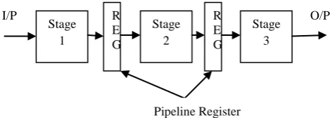
In HDLC, pipelining technique has been used which increases the performance by increasing the throughput and speed of the HDLC controller by performing multiple operations at the same time, but does not reduce instruction latency (the time to complete a single instruction from start to finish) as it still must go through all steps. Wireless sensor networks can increase the spatial and temporal resolution of operational data from pipeline infrastructures and thus address the challenge of near real-time monitoring and eventually control. The use of WSNs for monitoring large diameter bulk-water transmission pipelines has been focused. In pipeline architecture we cannot only speed up the clock but also the time taken by the design to process millions of instruction. In simple architecture without pipeline the next input have to wait until the current processing is completed where as in pipeline the whole process is divided into small process and next input will start after the current input is processed by first stage and also reduce the critical path.
In this paper, pipelining technique has been used with HDLC chip based on FPGA for better performance and throughput. In pipelining architecture N number of inputs are processed at the same time parallel. Pipelining Technique is applied in register module, where we use 8-bit register out of which each register is used for different purpose.
5.
PIPELINING
In a typical system speedup is achieved through parallelism at all stages such as user, multitasking, processing, multi-programming, and multi-threading. A technique used in advanced microprocessors where the microprocessor begins executing a second instruction before the first instruction has been completed. A Pipelining is a series of stages, where some work is done at each stage. To finish the work or any instruction, it has to pass through all stages. It does not reduce instruction latency i.e. the time to complete a single instruction from start to finish until it goes through all steps. Instead, it may increase latency by breaking the computation into separate steps and, the pipeline may stall furtherincreasing latency. Pipelining is frequently used in CPUs, but avoided in real time systems, where latency is a hard constraint.
[image:3.595.317.552.76.160.2]In pipelining we split each instruction into a sequence of steps and process each instruction parallel instead of processing one instruction at a time and finishing one at a time.
Fig. 2 Pipeline architecture
5.1
Data Flow in Pipelining
The data flow chat of pipelining is composed of six steps i.e. Instruction Fetch (IF), Instruction Decode (ID), Read Operands, Operation, Write Back Results, and fetching the next instruction from memory.
5.1.1
Instruction Fetch
The first step is Instruction Fetch. In this step instruction is fetched form the memory. The instruction and program counter (which is incremented) are stored in pipelined registers temporally.
5.1.2
Instruction Decode
The second step is Instruction Decode. The fetched instruction is decoded and various control lines are send to various part of the processor.
5.1.3
Instruction Execution
The third step is Instruction Execution or read operands. In this step any calculations are performed by ALU.
5.1.4
Memory Access
The fourth step is Memory Access or operation. In this stage storing and loading the values to and from the memory.
5.1.5
Write Back
The fifth step is Register Write Back. In this step the writing the results of a calculations to the register.
The sixth step is again fetching the instruction from the memory. And follow all the steps again for the next instruction
5.2
Design Consideration
The list of design consideration is given as below:
5.2.1
Speed
Pipelining reduces the processor cycle time and increase the throughput of instruction. The speed advantage is diminished to the extent that execution encounters hazards that require execution to slow below its ideal rate. A non-pipelined processor is a processor that executes only one instruction at a time. The next instruction will start after the completion of first instruction.
5.2.2
Economy
Pipelining make each step dependent and perform complex operations more economically. However, a processor that declines to pursue increased speed with pipelining may be simpler and cheaper to manufacture.
5.2.3
Predictability
Compared to environments where the programmer needs to avoid the hazards that come in pipelining, use of a non-pipelined processor may make it easier to program and to train programmers. The non-pipelined processor makes it easy by predicting the exact timing of a sequence of instructions [20].
6.
RESULTS AND DISCUSSION
HDLC implementation is done on Xilinx’s Spartan-3E and hardware simulation of HDLC chip based on FPGA is done on Modelsim SE 6.2c. The HDLC chip designed here supports two way communications simultaneously. Various real life scenarios have been created to see how different factors such as delay,
Stage 1
Stage 2
Stage 3 R
E G
R E G
Pipeline Register
frequency and area affect the performance of HDLC chip based on FPGA and Pipelining. Simulation of performance is carried out for HDLC chip based on FPGA in wireless sensor network. Throughput, average delay is used as performance metrics in this study.
Throughput: Throughput is defined as number of items such as cars, instructions and operations that exit the pipeline per unit time.
[image:4.595.50.299.245.676.2]Stage time: In general stage time is defined as the time taken by an instruction on non-pipelined machine per number of stages. The area (peak memory) of the chip gets increased because we need pipelined registers between different stages to store the values.
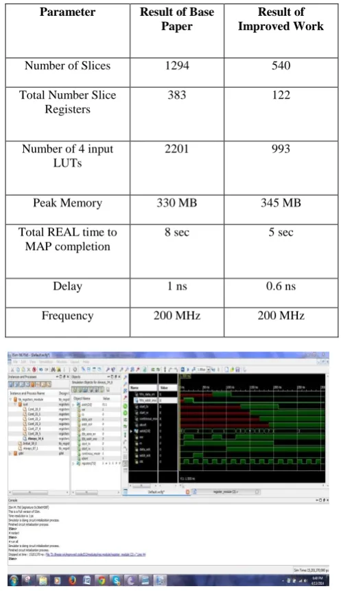
Table 1 Comparison between Base Paper and Improved Work
Parameter Result of Base Paper
Result of Improved Work
Number of Slices 1294 540
Total Number Slice Registers
383 122
Number of 4 input LUTs
2201 993
Peak Memory 330 MB 345 MB
Total REAL time to MAP completion
8 sec 5 sec
Delay 1 ns 0.6 ns
Frequency 200 MHz 200 MHz
Fig. 3 Simulation Waveform of Register Module
Fig. 4 Simulation Waveforms for HDLC Chip 1
Fig. 5 Simulation Waveforms for HDLC Chip 2
Simulation results show that the HDLC chip successfully realizes bidirectional data communication protocol with increased throughput of the overall circuit. The average throughput in pipeline is much better and delay and net skew is also reduced. The implementation of pipelining technique in HDLC Chip increases the speed of the circuit by implementing multiple instructions at the same time and not increasing the clock cycle.
We adopt pipelining technique in our existing design which is operated at the same clock frequency but this technique increase the speed of our system and reduce the delay and also increase the area of chip used. We reduce most of all the parameter by using this technique like delay and completion time etc.
7.
CONCLUSIONS
8.
ACKNOWLEDGMENT
The paper has been written with the kind assistance, guidance and active support of my department who have helped me in this work. I would like to thank all the individuals whose encouragement and support has made the completion of this work possible.
9.
REFERENCES
[1] L.Q. Zhauang, K. M. Goh and J. B. Zhang “The wireless sensor network factory automation: issues and challenges” IEEE International Conference 2007.
[2] Hong Luo, Cheng Chang, Yan Sun “Advanced Sensor Gateway based on FPGA for Wireless Multimedia Sensor Networks” IEEE International Conference 2011.
[3] Xilinx Application Note: “HDLC Controller Solutions with Spartan-II FPGAs” (v1.0) February 1, 2000.
[4] ISO/IEC 3309: 1993 (E), “Telecommunication and information exchange between system-high-level data link control (HDLC) procedures-Frame structure”.
[5] Ben Dewey “HDLC Derived Protocols” Xilinx Application Note SBE, Inc. 2001.
[6] Ms. Kshitija S. Patil, Prof. G. D. Salunke, Mrs. Bhavana L. Mahajan, Dr. A. S. Hiwale “Implementation of HDLC Protocol Using FPGA” International Journal of Engineering Science & Advanced Technology 2012.
[7] Jun Wang, Wenhao Zhang, Yuxi Zhang, Wei Wu “Design and Implementation of HDLC Procedures Based on FPGA” IEEE International Conference.
[8] Qasim, S.M.; Abbasi, S.A. “FPGA implementation of a single-channel HDLC Layer-2 protocol transmitter using VHDL” Microelectronics, 2003. ICM 2003 Proceedings of the 15th International Conference on 9-11.
[9] Gaurav Chandil;Priyanka Mishra;”Study and performance evaluation of Xilinx HDLC Controller and FCS Calculator”,vol.2,issue 10 (October 2012),PP 41-50.
[10]William Stallings, 2007. Data and Computer Communications, Eight Edition, Prentice Hall, pp: 222
[11]Amit Dhir, 2000. “HDLC Controller Solutions with Spartan-II FPGAs,” Xilinx Inc.
[12]Hong Luo Cheng Chang Yan Sun “Advanced Sensor Gateway based on FPGA for Wireless Multimedia Sensor Networks” IEEE internal Conference 2011.
[13]ZigBee Alliance, http://www.zigbee.org/.
[14]J. Song, S. Han, A. K. Mok et al., “WirelessHART: applying wireless technology in real-time industrial process control,” in Proceedings of the 14th IEEE Real-Time and Embedded Technology and Applications Symposium (RTAS '08), pp. 377–386, St. Louis, Mont, USA, April 2008. View at Publisher · View at Google Scholar · View at Scopus
[15]IPv6 over low power WPAN working group, http://tools.ietf.org/wg/6lowpan/.
[16]“ISA100, Wireless Systems for Automation,”http://www.isa.org/MSTemplate.cfm? MicrositeID=1134&CommitteeID=6891.
[17]P. Stig and C. Simon, “A survey of wireless sensor networks for industrial applications,” in The Industrial Electonics Handbook, Industrial Communication Systems, chapter 12, pp. 1–10, CRC Press, 2nd edition, 2011.
[18]D. M. Toma, J. del Rio, and A. Manuel-Lazaro, “Self-powered high-rate wireless sensor network for underground high voltage power lines,” in Proceedings of the 2012 IEEE International Instrumentation and Measurement Technology Conference (I2MTC '12), pp. 1881–1885, Graz, Austria, May 2012. View at Publisher · View at Google Scholar.
[19]Jakob Engblom “Processor Pipelines and Static Worst-Case Execution Time Analysis” ACTA Universitatis Upsaliensis Uppsala 2002.
[20]A description of the advanced scientific computer system, By: Austin, TEXAS INSTRUMENTS Inc.