Enhancement of Bandwidth in Microstrip Patch Antenna
using EBG
Neha Tyagi
Department of ECE Jaypee University, A-10, Sector-62, Noida (U.P.)-India
Shivani Singh
Department of ECE Jaypee University, A-10, Sector-62, Noida (U.P.)-India
Niti Sinha
Department of ECE Jaypee University, A-10,
Sector-62, Noida (U.P.)-India
ABSTRACT
This paper presents the bandwidth and gain enhancement of microstrip patch antenna using EBG for X band (10 Ghz) application. The surface waves must be suppressed to increase the bandwidth and gain by using EBG. By using EBG the stop band characteristics is created over certain frequency and that has been adapted to suppress the surface wave and to enhance the gain and bandwidth of the antenna at the resonating frequency. The main goal of using EBG structures in microstrip antenna is to achieve better gain and efficiency, lower side-lobes and back-lobes levels, and better isolations among array elements, by suppressing surface wave modes. The plot of return loss, gain and directivity with and without EBG are compared in this paper.By using patch antenna with EBG structure the operating bandwidth reaches 27% in the band of frequency 10.2-13GHz.
Index Terms
Bandwidth, Electromagnetic band gap, Gain, Microstrip patch antenna,directivity.
1. INTRODUCTION
With the advancement in the technologies the microstrip patch antennas comes out with best results for wireless devices because of its advantages like low profile, light weight, low cost and ease of fabrication. The size of patch should be around half a wavelength for the structure to work as good radiator[1].To overcome with the disadvantages of microstrip patch antenna i.e. excitation of surface wave, narrow bandwidth and low gain various techniques have been used namely micromachining [2,3], DGS(Defected ground structure)[4], periodic structures called electromagnetic bandgap (EBG)[5-8]. These methods have eliminated the bandwidth problem for most applications. But limitations of gain and surface wave excitation still remain. That is why, in recent years there has been considerable effort in the EBG structure for antenna application to suppress the surface wave and overcome the limitations of the antenna.The surface waves are reduced because of electromagnetic band gap created due to EBG structures. Recently ,there is a great interest in realizing the high efficiency patch antenna on high permittivity substrate, including the use of the latest micromachining technology [2].
In this paper, we propose a design based on concept of electromagnetic band gap (EBG) structures for enhancement of gain and bandwidth and compare the results with the edge feed microstrip patch antenna operating at 10 GHz resonating frequency for X band applications. The surface wave which are excited in the dielectric substrate are suppressed by placing square-lattice metal pads with grounding vias beneath
the patch, which not only improves the gain but also increase its frequency bandwidth. It has been shown in article [9] that, placing EBG cells in E-plane is suffcient for surface wave reduction and it is not required to have H-plane EBG cells. This EBG structures is used in microstrip array antennas between radiating array elements in E-plane to reduce mutual coupling between them by suppressing surface waves. But we are using EBG structures in both E-plane and H-plane over a single microstrip patch antenna. Our proposed antenna gives better performance compare to the conventional rectangular microstrip patch antenna. A substantial gain and bandwidth enhancement has been obtained. The design and simulation have been done by using Advanced Design System Simulator (ADS).
2.
ANTENNA
DESIGN
AND
STRUCTURE
DESCRIPTION
2.1 Microstrip patch antenna without ebg
For the known frequency and substrate parameters (h, ԑr and fo the size of antenna is calculated using the transmission line model. The equations for designing the patch antenna using transmission line model are given as[1]:
a. Width of patch
b. Effective dielectric constant
c. The extended patch length due to fringing field
d. The actual length
e. Effective length due to resonance
Fig 1.Microstrip patch without EBG structure in ADS tool
The patch antenna is feeded through various feeding technique as microstrip line feeding, inset feeding, coaxial feeding, proximity coupling feeding and aperture couple feeding [1]. We are using microstrip line feed of 50 ohm impedance with the ƛ/4 tranformer placed at the edge of patch on its width in this design. Fig 1 shows the proposed design of microstrip patch antenna on dieclectric substrate having dielectric constant =2.5 with height of substrate h=1.5mm,loss tangent=0.0022 and resonating frequency fo=10 GHz. By
using these substrate parameters the dimension of patch calculated as:
Length of patch L=8.37mm Width of patch w=11.338mm
The width of the patch should be chosen larger than the length of patch in order to get the higher bandwidth.The antenna is designed to operate at 10 GHz frequency.
2.2 Microstrip patch antenna with ebg
structures
Electromagnetic band gap structures are defined as artificial periodic objects that prevent/assist the propagation of electromagnetic waves in a specified band of frequency for all incident angles and all polarization states.Two commonly employed features are suppressing unwanted substrate modes and acting as an artificial magnetic ground plane. The main advantage of EBG structure is their ability to suppress the surface wave current. The generation of surface waves degrades the antenna efficiency and radiation pattern. Furthermore, it increases the mutual coupling of the antenna array which causes the blind angle of a scanning array EBG structures are periodic arrangement of dielectric materials and metallic conductors. They are categorized into three groups according to their geometric configuration: (a) three-dimensional volumetric structures, (b) two-three-dimensional planar surfaces, and (c) one-dimensional transmission lines[9]. In this proposed design we are using the 2-D mushroom type
EBG surfaces is shown in fig 3, which have the advantages of low profile, light weight, and low fabrication cost, and are widely considered in antenna engineering.
The parameters of the EBG structure are labeled in Fig. 2.a as patch width W, gap width g, substrate thickness h, dielectric constant εr, and vias radius r. When the periodicity (W + g) is
small compared to the operating wavelength, the operation mechanism of this EBG structure can be explained using an effective medium model with equivalent lumped LC elements, as shown in Fig.2b [10]. The capacitor results from the gap between the patches and the inductor results from the current along adjacent patches.The impedance of a parallel resonant LC circuit is given by:
The resonance frequency of the circuit is calculated as
following:
At low frequencies, the impedance is inductive and supports TM surface waves. It becomes capacitive at high frequencies and TE surface waves are supported. Near the resonance frequency wo, high impedance is obtained and the EBG does not support any surface waves, resulting in a frequency band gap.
[image:2.595.318.559.361.513.2](a) (b)
Fig 2. LC model for the mushroom-like EBG structure: (a) EBG parameters and (b) LC model[10]
The edge capacitance for the narrow gap situation is given by the following equation [10]:
The value of the inductor is derived from the current loop in Fig.2b, consisting of the vias and metal sheets. After a simple derivation, the inductance is expressed as below [10], which depends only on the thickness of the structure and the permeability:
L = μ h
The microstrip patch drawn on EBG substrate is shown in fig 3.In this proposed design we taking the parameter of EBG structure as:
c) The radius of via r= 0.4mm
and the other parameters like height of substrate and dielecetic constant is taken same as in case of microstrip patch antenna without EBG.
The width varies from 0.04ƛ GHz to 0.20ƛ GHz, gap width varies from 0.01ƛ GHz to 0.12ƛ GHz and the substrate thickness, h varies from 0.01ƛ GHz to 0.09ƛ GHz . Here, ƛ means the wavelength respect to the GHz range frequency.These parameters are directly effecting the performance of EBG that why they are dependent on wavelength.
[image:3.595.323.525.123.381.2]
Fig 3.Microstrip patch antenna with 2D EBG structure on ADS
3.
RESULTS
AND
DISCUSSION
It become easy to simulate the design through computer before real time implementation. The ADS tool helps us to determine the impedance bandwidth, return loss, gain and directivity.This simulator also helps to reduce the fabrication cost because only the antenna with the best performance would be fabricated.The simulated results of antenna with EBG and without EBG has been shown in fig 4 and fig 5.
3.1 Return loss and bandwidth
The return loss of patch antenna without EBG is -29.987db at10 GHz resonating frequency and return loss of proposed antenna with EBG is -42.34db at 10.67 GHz resonating frequency.The negative value of return loss signifies that there are significantly less losses in the antenna.
The bandwidth an be calculated from fig 4 and fig 5.The bandwidth of patch antenna without EBG is from 9.75-10.25
GHz i.e 4% and bandwidth of patch antenna with EBG is from 10.1-13 GHz which is 27.17%.The bandwidth of patch antenna with EBG is higher than the conventional patch antenna.
[image:3.595.55.285.211.529.2]Fig 4.Return loss of microstrip patch antenna without EBG with L=8.37mm, w=11.338mm, h=1.5mm and =2.5.
Fig 5.Return loss of microstrip patch antenna with EBG and with the same dimension as of conventional patch but width of metal pads W=5.5mm, gap width g=0.4mm and
[image:3.595.315.525.456.701.2]3.2 Gain and directivity
The antenna parameters of patch antenna without EBG and with EBG is shown in fig 6 and fig 7
[image:4.595.54.268.125.400.2]
Fig 6.Antenna parameters of microstrip patch antenna without EBG
Fig 7. Antenna parameters of microstrip patch antenna with EBG
The gain of patch antenna without EBG is 6.05db and of antenna with EBG is 7.64db.The directivity of patch antenna without EBG is 6.99dbi and of antenna with EBG is 9.64dbi.The gain and directivity of microstrip patch antenna with EBG is greater than conventional patch antenna.
-1 35°
-9
0
°
-45°
0°
45°
90°
135°
180° -31 -21 -11 -1
-41 9
THETA (-90.000 to 90.000)
M
a
g
.
[d
B
[image:4.595.339.517.156.367.2]i]
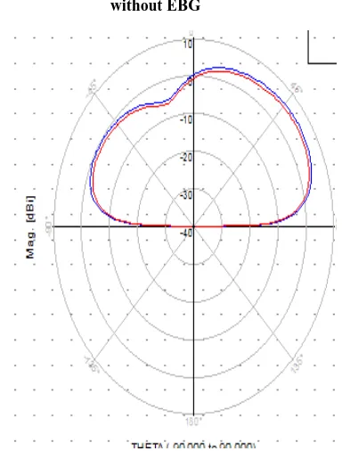
Fig 8.Gain and directivity of microstrip patch antenna without EBG
Fig.9.Gain and directivity of microstrip patch antenna with EBG
4.
CONCLUSION
[image:4.595.341.533.414.667.2] [image:4.595.54.272.452.713.2]than patch without EBG.The gain and bandwidth also improves when EBG is added on the patch.
5. REFERENCES
[1] Constantine A Balanis, Antenna Theory Analysis and Design, 2nd Edition, Singapore, John Wiley and Sons,2002.
[2] Gautheir, G. P., A. Courtay, and G. M. Rebiez, “Microstrip antennas on synthesized low dielectric constant substrate,” IEEE Trans. Ant. Propag., 1997. [3] Papalymerou I., R. F. Drayton, and L. P. B. Katehi,
“Micromachined patch antennas,”IEEE Trans. Ant. Propag., Vol. 46, No. 2, 275- 283, 1998.
[4] Ashwini K. Arya, M.V.Kartikeyan, Patnaik,A.,“Defected ground structure in the perspective of microstrip antennas: A review”, Frequenz, Int.Journal of
RF-Engineering and Telecommunication , vol. 64, no.5-6, pp. 79-84, 2010.
[5] Qian Y., R. Coccioli, D. Sievenpiper, V. Radisic, E. Yablonovich, and T. Itoh, “Microstrip patch antenna using novel photonic bandgap structures,” Microw. J., Vol. 42, No. 1, 66-76,1999.
[6] Coccioli R., F. R. Yang, K. P. Ma, and T. Itoh, “Aperture coupled patch antenna on UC-PBG substrate,”IEEE Trans. Microw. Theory Tech., Vol. 47, No. 11, 2123-2130, 1997.
[7] Yang A. F. and Y. Rahmat-Sami, “A low-profile circularly polarized curl antenna over an electromagnetic band gap (EBG) surface,” Microw. Opt. Technol. Lett., Vol. 31, No. 4, 2001.
![Fig 2. LC model for the mushroom-like EBG structure: (a) EBG parameters and (b) LC model[10]](https://thumb-us.123doks.com/thumbv2/123dok_us/8048109.773207/2.595.318.559.361.513/fig-model-mushroom-like-ebg-structure-parameters-model.webp)