International Journal of Emerging Technology and Advanced Engineering
Website: www.ijetae.com (ISSN 2250-2459,ISO 9001:2008 Certified Journal, Volume 3, Issue 7, July 2013)
508
Performance Analysis of Improved Double Flying Capacitor
Multicell Converter
Amal Philomiya L
1, Saravanan.C
2, Narasimman.P
3 1PG Scholar, 2Assistant Professor, Sudharsan Engg. College, Sathiyamangalam, Pudukkottai.
3Assistant Professor, Kings Engg.College, Punalkulam, Tanjavur
.
Abstract—Multilevel converters are very interesting
alternatives for medium and high-power applications. Here we developed an improved configuration of double flying capacitor multicell(DFCM) converter. The benefits of this new converter comparing with conventional DFCM, are doubling of the number of output voltage levels and improving the output voltage frequency spectrum. The conventional configuration is modified by additionally two low power switches and one dc voltage source having small fraction of voltage rating with main dc-link voltage rating. The doubling output voltage levels in the new converter creates it possible to decrease the number of cells , flying capacitors, their voltage rating and the amount of stored energy. This converter is controlled by a phase-shifted carrier pulsewidth modulation technique .Simulation results are presented to validate the effectiveness of the proposed converter. Additionally, measurements taken from an experimental setup are presented in order to study the practical configuration. Futhuremore switching losses and total harmonic distortion are calculated
I. INTRODUCTION
All Numerous industrial applications have begun to require higher power apparatus in recent years[10]. Some medium voltage motor drives and utility applications require medium voltage and megawatt power level. For a medium voltage grid, it is troublesome to connect only one power semiconductor switch directly. As a result, a multilevel power converter structure has been introduced as an alternative in high power and medium voltage situations. A multilevel converter not only achieves high power ratings, but also enables the use of renewable energy sources. Renewable energy sources such as photovoltaic, wind, and fuel cells can be easily interfaced to a multilevel converter system for a high power application. The concept of multilevel converters has been introduced since 1975.[1] The term multilevel began with the three-level converter. Subsequently, several multilevel converter topologies[5][6] have been developed.
However, the elementary concept of a multilevel converter to achieve higher power is to use a series of power semiconductor switches with several lower voltage dc sources to perform the power conversion by synthesizing a staircase voltage waveform. Capacitors, batteries, and renewable energy voltage sources can be used as the multiple dc voltage sources. The commutation of the power switches aggregate these multiple dc sources in order to achieve high voltage at the output; however, the rated voltage of the power semiconductor switches depends only upon the rating of the dc voltage sources to which they are connected.
Flying-capacitor-based converters have many attractive properties for medium voltage applications including natural selfbalancing, transformerless operation, and equal distribution of voltage stress between semiconductor switches.[7][8][9]
The mentioned advantages of flyingcapacitor- based converters such as Flying capacitor multicell(FCM) and Stacked multicell(SM) converters, their bulky and costly flying capacitors are the main problems of these converters especially when the number of cells increases. In [2] proposed a configuration called double flying capacitor multicell (DFCM) converter in which the number of flying
capacitors and their voltage rating are reduced
International Journal of Emerging Technology and Advanced Engineering
Website: www.ijetae.com (ISSN 2250-2459,ISO 9001:2008 Certified Journal, Volume 3, Issue 7, July 2013)
509
II. IMPOVED CONFIGURATION OF ADOUBLE FLYING CAPACITOR MULTICELL CONVERTER
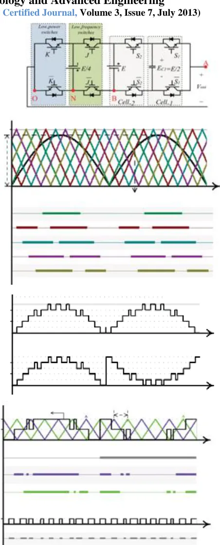
In this paper, the improved configuration of a DFCM converter is proposed to reduce the number and voltage rating of flying capacitors and as a result, decrease the size and cost of the converter. Fig. 1 shows the proposed 11-level I-DFCM converter which only uses one flying capacitor, while it is required to use nine, eight, and four flying capacitors, respectively, to produce the same number of levels utilizing FCM, SM, and DFCM converters. Moreover, the total voltage rating of flying capacitors and dc-link capacitors to produce the single-phase 11-level
output voltage with the peak-to-peak voltage of 10E is 55E,
30E, and 15E in FCM, SM, and DFCM converters,
respectively, while it is 7E in the proposed configuration of
an I-DFCM converter
A. Operation
As shown in Fig. 1,which illustrates the operational principles of an I-DFCM converter, one minor dc voltage
source with the voltage rating of E/4 (equal to half of the
voltage rating of the smallest and the most right flying capacitor) and two complimentary low-power high-frequency switches are added to the most left part of the DFCM converter. The main duty of added minor dc voltage
source as well as two switches of K and K1 is to produce
the minor voltage levels, i.e., odd levels, between the major voltage levels, i.e., even levels, produced by DFCM
converter. Two added switches of K and K1 make it
possible that the minor dc voltage source to be connected in series with the major dc voltage source and therefore, produces the small steps and increases the number of output voltage levels. As a result, the minor converter which includes the minor dc voltage source and two
low-power switches produces only the minor levels of −1, 0,
and +1 in series with the main DFCM converter which
produces −4, −2, 0, +2, and +4, i.e., even levels; thus, the
proposed I-DFCM converter, as sum of minor and major
converters, in total produces 11 levels from −5 to +5 in one
unit steps.
B. Generation of Switching States
As shown in Fig. 1, Vref ,abs , which is the absolute value
of output reference voltage Vref, is intersected and
compared with five phase-shifted carriers. As seen, the
[image:2.612.328.554.112.670.2]output of comparator #Y is 1
International Journal of Emerging Technology and Advanced Engineering
Website: www.ijetae.com (ISSN 2250-2459,ISO 9001:2008 Certified Journal, Volume 3, Issue 7, July 2013)
510
When the Vref ,abs is higher than the carrier #Y and is 0
when the Vref ,abs is lower than the carrier #Y. Then, the
output of comparators are added together to generate the
output reference voltage in a staircase waveform Vref ,abs,s
. The notation of abs and s refer to absolute value and staircase waveform respectively. Afterward, the modified
output reference voltage(called Vref -mdf ) can be generated
as follows:
Vref ,mdf = Vref ,abs,s. sgn (Vref) +(1 − sgn (Vref ) /2*5 (1)
Where sgn (x)is the signum function and equals +1 when
the signal x is positive and equals −1 when the signal x is
negative. According to the modified output reference
voltage Vref -mdf , the reference of a DFCM converter Vref
-DFCM is calculated to produce the major levels of 0, +2, and
+4, i.e., even levels. In In other words, Vref -DFCM can be
expressed
Vref-DFCM= 2*[(Vref -mdf )/2] (2)
Where, [ ] indicates the floor function and [x] is the
integer part of x. After this calculation, the reference of a
DFCM converter Vref-DFCM is intersected with two
phase-shifted carriers to determine the states of DFCM
converter‟s switches, i.e., J, S2 , and S1 . In the next step,
as shown in Fig. 1, Vref -DFCM is subtracted from V
ref-mdf to calculate the status of switch K. If the result of
subtraction is 1, the switch K is ON and if the result of
subtraction is 0, the switch K is OFF. It should be noted
that switches K and K 1are complimentary. To make the
[image:3.612.314.571.112.427.2]operational principle of an I-DFCM converter much more comprehensible, the switching states of a two-cell-11-level I-DFCM converter are illustrated in Table I.
Table 1
Switching States Of The Proposed Two-Cell 11-Level I-Dfcm Converter
Output voltage level
J K S2 S1 No. of
states
+5E/4 0 1 1 1 1
+4E/4 0 0 1 1 1
+3E/4 0 1 0 1 2
1 1 0
+2E/4 0 0 0 1 2
0 1 0
+1E/4 0 1 0 0 1
0 0 0 0 0 2
1 1 1
-1/4 1 0 1 1 1
-2E/4 1 1 0 1 2
1 1 0
-3E/4 1 0 0 1 2
0 1 0
-4E/4 1 1 0 0 1
-5E/4 1 0 0 0 1
III. ANALYSIS
A . Switching loss caculation
Consider a single MOSFET switch connected across a
dc voltage of value Vdc. Current through switch during
„on‟ time is considered as Idc. the waveforms of t the
voltage across and the current through the switch when it is
operated at a switching frequency of Fs=1/Ts, where Ts is
the switching period. To simplify the expression, the
switching waveforms are represented by linear
approximations. In the figure, Vm and Imare the voltage and
International Journal of Emerging Technology and Advanced Engineering
Website: www.ijetae.com (ISSN 2250-2459,ISO 9001:2008 Certified Journal, Volume 3, Issue 7, July 2013)
511
Switching losses can be calculated from the turn-on and turn-off characteristics of the devices. Instantaneous
voltage and current during turn-on time tc(on) are
v(t)=Vdc-(Vdc-Von)*(t/tc(on)); 0<t≤tc(on) ...(1)
i(t)=Idc*(t/tc(on)) 0 < t ≤ tc(on) ...(2)
Instantaneous power during the interval tc(on) is,
p(t)=v(t)*i(t)
={ Vdc-(Vdc-Von)*(t/tc(on))}*{ Idc*(t/tc(on))}
={Vdc*Idc*(t/tc(on))}-(Vdc-Von)*Idc*(t2/t2c(on)) …(3)
And energy dissipated during this interval is tc(on),
Ec,on=∫[ {Vdc *Idc*(t/tc(on))} – (Vdc-Von)*Idc*(t2/t2c(on)) ]dt
0 to tc(on)
Ec,on= (Vdc *Idc*tc(on))/2-(Vdc-Von)*Idc*tc(on)/3
=(Vdc*Idc*tc(on))/6-(Von*Idc*tc(on))/3 …(4)
And during turn-off transition, of tc(off), the current falls
Idc to zero and the Von rises linearly to Vdc. The
instantaneous voltage and current during this period are,
V(t)=Von+(Vdc-Von)*(t/tc(off)) …..(5)
i(t)=Idc-Idc*(t/tc(off)) …..(6)
The instantaneous power dissipated during the interval tc(off) is ,
p(t)=v(t)*i(t)
={ Von +(Vdc-Von)*(t /tc(off))}*{ Idc -Idc *(t/tc(off))}
= Von* Idc+ (Vdc-Von) * Idc *(t /tc(off))- Von* Idc
*(t/tc(off))-(Vdc-Von)*Idc*(t/tc(off))2 ….(7)
Hence, the energy dissipated can be found as tc(off),
Ec,off=∫[ Von* Idc+ (Vdc-Von) * Idc *(t /tc(off))- Von* Idc
*(t/tc(off))-(Vdc-Von)* Idc * (t /tc(off))2]dt 0 to tc(off)
=(Vdc*Idc*tc(off))/6-(Von*Idc*tc(off))/3 ….(8)
With a switching frequency of Fs, the average switching
loss in the switch during each transition of turn-on and turn-off can be found as,
Pc,on=(Vdc*Idc*tc(on)/Ts)/6-(Von*Idc*tc(on)/Ts)/3 ...(9)
Pc,off=(Vdc*Idc*tc(off)/Ts)/6-(Von*Idc*tc(off)/Ts)/3 .. (10)
Hence, the average switching loss Psw in the switch is,
Psw=(1/6)*(Vdc *Idc*{tc(on +tc(off)}/Ts)+(1/3)* (Von*Idc*
{tc(on+tc(off)}/T) …..(11)
[image:4.612.332.557.275.416.2]Eqn.(11) shows that the switching power loss in a semi-conductor switch varies linearly with the switching frequency and switching times. Therefore, with the devices having short switching times, it is possible to operate them at a higher switching frequency thus avoiding excessive switching power losses in the device. The losses are calculated for the corresponding switching states from TABLE I.
Fig 2 Linearised switching characteristic of controllable switch (IGBT/MOSFET).
IV. SIMULATION RESULTS
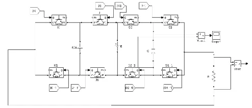
In this section, simulation results of the proposed 11-level I-DFCM converter are provided to verify its good performance and switching pattern using MATLAB simulink.
A. Simulation Models
[image:4.612.329.576.549.655.2]International Journal of Emerging Technology and Advanced Engineering
Website: www.ijetae.com (ISSN 2250-2459,ISO 9001:2008 Certified Journal, Volume 3, Issue 7, July 2013)
512
Fig 4 V ref DFCM circuit
Fig 5 Switching states
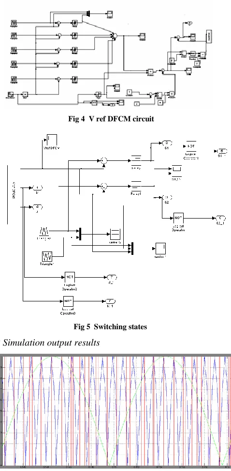
B Simulation output results
Fig 6 . Five phase shifted carriers
Fig 7 Vref,abs,s output waveform
Fig 8 Vref,mdf output waveform
[image:5.612.54.293.135.621.2] [image:5.612.324.576.297.592.2]International Journal of Emerging Technology and Advanced Engineering
Website: www.ijetae.com (ISSN 2250-2459,ISO 9001:2008 Certified Journal, Volume 3, Issue 7, July 2013)
[image:6.612.321.578.114.259.2]513
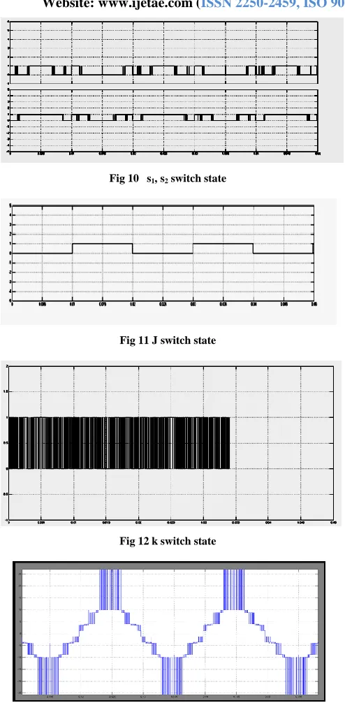
[image:6.612.48.295.123.626.2]Fig 10 s1, s2 switch state
Fig 11 J switch state
Fig 12k switch state
Fig 13 Two cell 11 level proposed I – DFCM Converter’s Output Waveform
Fig 14 Two cell 11 level proposed I – DFCM Converter’s Total Harmonic Distortion
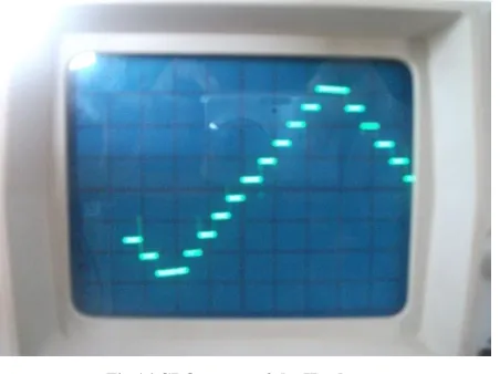
V. EXPERIMENTAL RESULTS
To test validity and praticallity of the proposed configuration a prototype two cell 11-level proposed I – DFCM was built with eight IRF 840, 8A, 400V MOFETs as shown in figure15. The flying capacitors values are 1000mF, fundamental frequency is 50Hz with resistive load.
[image:6.612.328.576.380.541.2]International Journal of Emerging Technology and Advanced Engineering
Website: www.ijetae.com (ISSN 2250-2459,ISO 9001:2008 Certified Journal, Volume 3, Issue 7, July 2013)
[image:7.612.58.284.136.305.2]514
Fig 16 CRO output of the Hardware
The match between simulation and experimental results confirms the advantages and practicality of the proposed I-DFCM converter and its control strategy.
VI. CONCLUSION
This paper proposes a new configuration called the I-DFCM converter to decrease the number of cells and flying capacitors as well as the flying capacitors‟ voltage ratings. This results in a reduction of the cost and size of the flying-capacitor-based converters and makes them more practical. Both simulation and experimental results demonstrate the good performance and feasibility of the proposed converter.
REFERENCES
[1] L. G. Franquelo, J. Rodriguez, J. I. Leon, S. Kouro, R. Portillo, and M. A. M. Prats, “The age of multilevel converters arrives,” IEEE Ind. Electron. Mag., vol. 2, no. 2, pp. 28–39, Jun. 2008.
[2] A. K. Sadigh, S. H. Hosseini, M. Sabahi, and G. B. Gharehpetian, “Double flying capacitor multicell converter based on modified phase-shifted pulse Width modulation,” IEEE Trans. Power Electron., vol. 25, no. 6, pp. 1517–1526, Jun. 2010.
[3] E. Babaei, “A cascade multilevel converter topology with reduced number of switches,” IEEE Trans. Power Electron., vol. 23, no. 6, pp. 2657–2664, Nov. 2008.
[4] T. A. Meynard, H. Foch, F. Forest, C. Turpin, F. Richardeau, L. Delmas, G. Gateau, and E. Lefeuvre, “Multicell converters: Derived topologies,”IEEE Trans. Ind. Electron., vol. 49, no. 5, pp. 978–987, Oct. 2002.
[5] R. Wilkinson, H. du Mouton, and T. Meynard, “Natural balance of multicell converters: The general case,” IEEE Trans. Power Electron., vol. 21, no. 6, pp. 1658–1666, Nov. 2006.
[6] A. Shukla, A. Ghosh, and A. Joshi, “Flying-capacitor-based chopper circuit for dc capacitor voltage balancing in diode-clamped multilevel inverter,” IEEE Trans. Ind. Electron., vol. 57, no. 7, pp. 2249–2261, Jul. 2011.
[7] C. Feng, J. Liang, and V. G. Agelidis, “Modified phase-shifted PWM control for flying capacitor multilevel converters,” IEEE Trans. Power Electron., vol. 22, no. 1, pp. 178–185, Jan. 2007. [8] R. Wilkinson, H. du Mouton, and T. Meynard, “Natural balance of
multicell converters: The two-cell case,” IEEE Trans. Power Electron., vol. 21, no. 6, pp. 1649–1657, Nov. 2006.
[9] T. Meynard,H. Foch, P. Thomas, J. Courault, R. Jakob, andM.Nahrstaedt, “Multicell converters: Basic concepts and industry applications,” IEEE Trans. Ind. Electron., vol. 49, no. 5, pp. 955– 964, Oct. 2002.
[10] Ned M.,Undeland, T.M., Robbins,WP:”Power electronics converter, applications and design”(John Willey&Sons,2001,3rd edn.)
[11] Rashid,M..H.”Powerelectronicshandbook”(Academic Press Newyork,20013rd edn.)