http://www.scirp.org/journal/gsc ISSN Online: 2160-696X
ISSN Print: 2160-6951
Effects of PBr
3
Addition to Polysilane Thin
Films on Structures and Photovoltaic
Properties
Junya Nakagawa1, Takeo Oku1*, Atsushi Suzuki1, Tsuyoshi Akiyama1,
Masahiro Yamada2, Sakiko Fukunishi3, Kazufumi Kohno3
1Department of Materials Science, The University of Shiga Prefecture, Hikone, Japan 2Osaka Gas Co., Ltd., Osaka, Japan
3Osaka Gas Chemicals Co., Ltd., Osaka, Japan
Abstract
Organic thin film solar cells are potential next generation solar cells. Many p-type semiconductors have been used in organic solar cells, but there have been far fewer reports involving n-type organic semiconductors. Developing new n-type organic semiconductors is therefore desirable. Polysilane thin films were spin-coated from solutions containing phosphorus (P), and the ef-fects of P addition on film microstructures and electronic properties as n-type semiconductors were investigated. Microstructures of poly-methyl-phenyl- silane (PMPS), dimethyl-polysilane (DMPS) and deca-phenyl-penta-silane (DPPS) thin films were investigated by X-ray diffraction and transmission electron microscopy. PMPS thin films doped with P (PMPS(P)) were amorphous upon annealing at 300˚C, while DMPS(P) and DPPS(P) thin films exhibited crystalline structures. PMPS(P) and DMPS(P) thin films exhibited decreased electrical resistances upon P doping. The energy gaps of PMPS(P), DMPS(P) and DPPS(P) were 3.5, 3.9 and 3.8 eV, respectively. Decreased pho-toluminescence intensities of PMPS, DMPS and DPPS were observed upon P doping. The desorption of phenyl and methyl groups from PMPS(P) thin films was observed from Raman scattering measurements. Solar cells con-taining polysilane(P)/poly[3-hexylthiophene] heterojunction structures were fabricated and exhibited photovoltaic behavior.
Keywords
Microstructure, Thin Film, Property, Polysilane, Solar Cell
1. Introduction
Solar cells are a promising clean energy alternative to fossil fuels. The
produc-How to cite this paper: Nakagawa, J., Oku, T., Suzuki, A., Akiyama, T., Yamada, M., Fukunishi, S. and Kohno, K. (2017) Effects of PBr3 Addition to Polysilane Thin Films
on Structures and Photovoltaic Properties.
Green and Sustainable Chemistry, 7, 20-34. https://doi.org/10.4236/gsc.2017.71002
Received: December 22, 2016 Accepted: February 7, 2017 Published: February 10, 2017
Copyright © 2017 by authors and Scientific Research Publishing Inc. This work is licensed under the Creative Commons Attribution International License (CC BY 4.0).
http://creativecommons.org/licenses/by/4.0/
tion cost of current silicon solar cells is high, and reducing the cost of solar cells is a priority. To this end, organic semiconductor based solar cell are potential next generation solar cells. Organic thin film solar cells are economical to pro-duce, flexible and light weight, and their photovoltaic and optical properties
have been much studied [1][2][3][4]. Many p-type semiconductors have been
used in organic solar cells, but there have been far fewer reports involving n-type organic semiconductors. Developing new n-type organic semiconductors is an important next step.
Polysilane materials are p-type semiconductors, and have been applied as
conducting materials in photovoltaic systems [1]-[7]. Polysilanes are organic
polymers containing main chain Si-Si bonds and side chain organic substituents. They exhibit σ-conjugation along the Si main chain, and their hole mobility is
ca. 10−4 cm2∙V−1∙s−1[1]. Polysilane Si main chains are similar to σ-bonded
polyo-lefin C-C chains. Polysilanes possess a 3p orbital and an enlarged σ-orbital, compared with polyolefins with their 2p orbital. Polysilanes can potentially be applied as p-type semiconductors in organic thin film solar cells, but few studies
on polysilane solar cells have been reported [1] [8][9][10]. Doped polysilanes
can act as n-type semiconductors, and while they have been applied in organic
solar cells, further investigation is needed [11][12].
Herein, polysilane thin films were spin-coated from solutions of poly-methyl- phenyl-silane (PMPS), dimethyl-polysilane (DMPS) and deca-phenyl-penta-silane (DPPS) with phosphorus (P). The effect of P addition on film microstructures and electronic properties as n-type semiconductors were investigated. Spin- coating is economical and applicable to the mass production of thin films. Light induced carrier separation and charge transfer was investigated from ultravio-let-visible (UV-vis) absorption and photoluminescence measurements. The ef-fects of P addition were investigated from current density-voltage (J-V) charac-teristics, UV-vis absorption and photoluminescence measurements and Raman
scattering spectra [13] [14] [15]. Film microstructures were investigated by
X-ray diffraction (XRD) and transmission electron microscopy (TEM).
2. Experimental Procedures
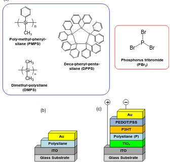
Figure 1(a) shows the molecular structures of PMPS, DMPS, DPPS and
phos-phorus bromine (PBr3) which was used as the P dopant. Indium tin oxide (ITO)
glass plates (Xin Yan Technology, ~10 Ω/□) were ultrasonically cleaned with
acetone and methanol, and dried under N2. Figure 1(b) depicts a polysilane thin
film deposited on a substrate. PBr3 (0.05 mL, Wako) and PMPS or DPPS (24 mg,
Osaka Gas Chemicals) or DMPS (24 mg, Strem Chemicals) were added to 1 mL
of o-dichlorobenzene [8]. The resulting solution was spin-coated at 1000 rpm,
and the substrate then annealed at 300˚C for 10 min under N2. Au contacts were
vacuum-evaporated as the top electrode.
The structure of solar cells is shown in Figure 1(c). ITO glass plates were
cleaned as above. TiOx thin films were prepared by a sol-gel procedure, in which
Figure 1. (a) Structures of PMPS, DMPS, DPPS and PBr3. (b) Structure of polysilane thin
film deposited on substrate. (c) Structure of polysilane(P)/P3HT heterojunction solar cell.
The resulting TiOx precursor solution was spin-coated on the ITO substrate in
air, and the substrate annealed at 140˚C for 60 min in air. PBr3 (0.02 mL) and
polysilane (24 mg) were added to 1 mL of o-dichlorobenzene, and the resulting solution spin-coated on the substrate at 1000 rpm.
The substrate was annealed at 300˚C for 10 min in N2. Poly[3-hexylthiophene]
(P3HT) (Sigma Aldrich) was spin-coated on the substrate at 1000 rpm, and the substrate annealed at 300˚C for 10 min in air. Poly(3,4-ethylenedioxylenetthi- ophene): polystyrene sulfonic acid (PEDOT:PSS) was spin-coated on the sub-strate at 2000 rpm. Au contacts were vacuum-evaporated as the top electrode.
The final device was annealed at 140˚C for 10 min under N2.
Polysilane thin film microstructures were investigated by XRD (Philips, X’pert-MPD) with CuKα radiation operated at 40 kV and 40 mA, and TEM
(Hi-tachi, H-8100) operated at 200 kV. J-V characteristics were measured using a
Hokuto Denko, HSV-110 apparatus in the dark, and using an AM 1.5 solar si-mulator (San-ei Electric, XES-301S).
Optical properties were investigated by UV-vis absorption spectroscopy (Jas-co, V-670). Photoluminescence measurements were recorded using a Hitachi F-4500 spectrofluorometer. Film thicknesses were measured by atomic force microscopy (AFM; SII SPA400). Thin film carrier concentrations and mobilities were estimated using the Hall effect measurement system (Toyo, ResiTest 8320).
Poly-methyl-phenyl-silane (PMPS)
Dimethyl-polysilane (DMPS)
Si
CH3
n
Deca-phenyl-penta-silane (DPPS)
Si Si Si Si
Si
Si
CH3 CH3
n
Phosphorus tribromide (PBr3)
P Br
Br Br
(a)
Glass Substrate ITO Polysilane
Au
+ -
Glass Substrate ITO
TiOx Polysilane (P)
P3HT PEDOT:PSS
Au
Raman scattering spectra were recorded with a Raman laser spectrometer (Jasco, NRS-5100). Raman modes and optical images were observed using an excitation laser wavelength of 532 nm.
3. Results and Discussion
3.1. Microstructures of Thin Films
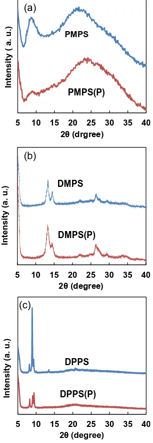
[image:4.595.298.451.254.695.2]XRD patterns of PMPS, DMPS and DPPS thin films after annealing are shown in Figure 2. PMPS did not exhibit sharp diffraction peaks, while DMPS and DPPS did. A broad peak at 2θ of 8.7˚ was observed for PMPS, which disappeared upon
addition of PBr3. The diffraction pattern of the P doped PMPS (PMPS(P)) thin
film indicated the crystalline structure became amorphous upon doping.
Figure 2. XRD patterns of annealed thin films of (a) PMPS, (b) DMPS and (c) DPPS thin films, with and without P doping.
5 10 15 20 25 30 35 40
In
te
n
s
ity
(a
. u
.)
2θ (degree)
5 10 15 20 25 30 35 40
In
te
n
s
ity
(a
. u
.)
2θ (degree)
5 10 15 20 25 30 35 40
In
te
n
s
ity
( a
. u
.)
2θ (drgree)
DMPS
DMPS(P)
PMPS
PMPS(P)
DPPS
DPPS(P) (a)
(b)
Diffraction peaks at 2θ of 13˚, 14˚ and 26˚ were observed for DMPS, and their intensity increased upon P doping. Diffraction peaks at 2θ of 8.2˚, 8.9˚, 9.4˚ and 13˚ were observed for DPPS, and their intensity decreased upon P doping. The XRD results indicate that DMPS and DPPS thin films were crystalline. Doping PMPS with P enhanced the decomposition of PMPS, facilitated the formation of the amorphous structure. The structure of DMPS contains less steric hindrance than that of PMPS, which accounts for the more crystalline nature of the DMPS thin film.
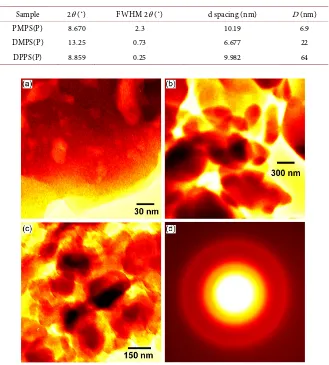
Crystallite sizes (D) of PMPS(P), DMPS(P) and DPPS(P) thin films are
sum-marized in Table 1. D values were estimated from Scherrer’s equation:
0.9 cos ,
D= λ B θ (1)
where λ, B and θ represent the X-ray source wavelength, full width at half max-imum (FWHM) and Bragg angle, respectively. D values of PMPS(P), DMPS(P) and DPPS(P) thin films were 6.9, 22 and 64 nm, respectively.
[image:5.595.210.539.341.706.2]Figure 3 shows TEM images of PMPS(P), DMPS(P) and DPPS(P) thin films,
Table 1. Structural parameters from XRD patterns of PMPS(P), DMPS(P) and DPPS(P) thin films.
Sample 2θ (˚) FWHM 2θ (˚) d spacing (nm) D (nm)
PMPS(P) 8.670 2.3 10.19 6.9
DMPS(P) 13.25 0.73 6.677 22
DPPS(P) 8.859 0.25 9.982 64
and an electron diffraction pattern of PMPS(P). The polysilanes possessed na-noparticle structures, and the electron diffraction pattern of PMPS(P) indicated a relatively amorphous structure.
3.2. Electronic and Optical Properties of Thin Films
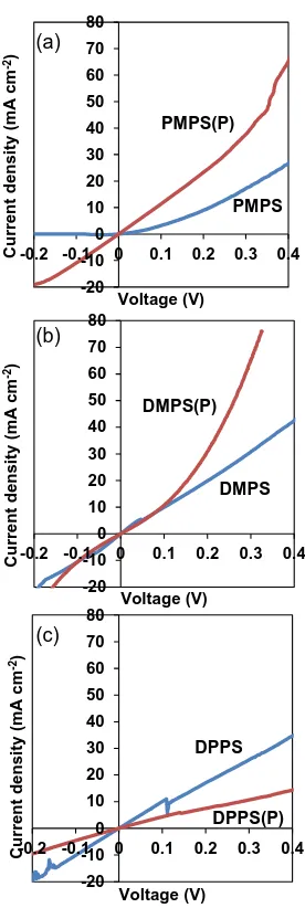
[image:6.595.304.442.214.625.2] [image:6.595.208.541.675.733.2]J-V characteristics of polysilane thin films measured in the darkare shown in Figure 4. Table 2 shows electrical resistances of polysilane thin films calculated at +0.20 V. PMPS(P) and DMPS(P) thin films exhibited decreased electrical re-sistances upon P doping. PMPS(P) exhibited n-type behavior, with a carrier
Figure 4. J-V characteristics of (a) PMPS, (b) DMPS and (c) DPPS thin films in the dark.
Table 2. Electrical resistances of undoped and P doped polysilane thin films.
Sample Resistance (Ωcm2) Resistance (Ωcm2) after P doping
PMPS 20 10
DMPS 11 7.7
DPPS 12 33
-20 -10 0 10 20 30 40 50 60 70 80
-0.2 -0.1Cu 0 0.1 0.2 0.3 0.4
rr
e
n
t d
e
n
s
ity
(m
A
c
m
-2)
Voltage (V) -20
-10 0 10 20 30 40 50 60 70 80
-0.2 -0.1 0 0.1 0.2 0.3 0.4
C
u
rr
e
n
t d
e
n
s
ity
(m
A
c
m
-2)
Voltage (V) -20
-10 0 10 20 30 40 50 60 70 80
-0.2 -0.1 0 0.1 0.2 0.3 0.4
C
u
rr
e
n
t d
e
n
s
ity
(m
A
c
m
-2)
Voltage (V)
DMPS DMPS(P)
PMPS PMPS(P)
DPPS
DPPS(P)
(a)
(b)
concentration and electron mobility of 1.0 × 1019 cm−3 and 2.4 cm2·V−1·s−1, re-spectively.
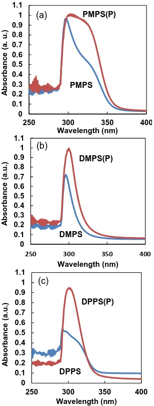
Figure 5 shows UV-vis absorption spectra of PMPS, DMPS and DPPS thin films after annealing. All three exhibited obvious absorptions at 300 - 400 nm, which increased in intensity upon doping. This suggests that increased photo absorption arose from the desorption of phenyl and methyl groups, from side chains in PMPS, DMPS and DPPS.
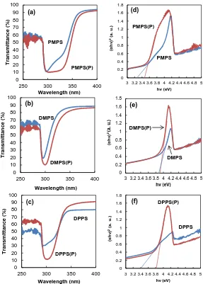
Transmittance spectra of PMPS, DMPS and DPPS thin films after annealing
are shown in Figure 6. Film thicknesses were estimated to be ca. 1 μm from
AFM measurements. Tauc plots show (αhν)2 versus hν values for PMPS, DMPS
and DPPS thin films after annealing. Optical absorption coefficients (α) were determined from the spectral transmittance by:
( )
1dln 1T ,α = (2)
Figure 5. UV-vis absorption spectra of (a) PMPS, (b) DMPS and (c) DPPS thin films, with and without P doping.
0 0.1 0.2 0.3 0.4 0.5 0.6 0.7 0.8 0.9 1 1.1
250 300 350 400
A
b
s
o
rb
a
n
c
e
(a
.u
.)
Wavelength (nm)
0 0.1 0.2 0.3 0.4 0.5 0.6 0.7 0.8 0.9 1 1.1
250 300 350 400
A
b
s
o
rb
a
n
c
e
(a
.u
.)
Wavelength (nm) 0
0.1 0.2 0.3 0.4 0.5 0.6 0.7 0.8 0.9 1 1.1
250 300 350 400
A
b
s
o
rb
a
n
c
e
(a
. u
.)
Wavelength (nm)
(a)
(b)
(c)
PMPS PMPS(P)
DMPS DMPS(P)
where d and T are the film thickness and transmittance, respectively [16].
Opti-cal band gap energies (Eg) were determined from:
(
g)
2 ,h A h E n
α ν = ν− (3)
[image:8.595.230.517.198.599.2]where h is Planck’s constant, ν is the frequency and n depends on the nature of the transition. n was found to be 1, corresponding to direct band to band transi-tion. The intersection of the straight line with the hν axis determines the value of Eg. Table 3 shows Eg values of polysilane thin films with and without P doping.
Figure 6. Optical transmission spectra of (a) PMPS, (b) DMPS and (c) DPPS thin films, with and without P doping. Tauc plots for (d) PMPS, (e) DMPS and (f) DPPS thin films with P doping.
Table 3. Energy gaps (Eg) of undoped and P doped polysilane thin films.
Sample Eg (eV) Eg (eV) after P doping
PMPS 3.3 3.5
DMPS 3.9 3.9
DPPS 3.4 3.8
0 0.2 0.4 0.6 0.8 1 1.2 1.4 1.6 1.8
3 3.2 3.4 3.6 3.8 4 4.2 4.4 4.6 4.8 5
(α hv ) 2(a . u .) hv (eV) 0 0.2 0.4 0.6 0.8 1 1.2 1.4 1.6 1.8
3 3.2 3.4 3.6 3.8 4 4.2 4.4 4.6 4.8 5
(α hv ) 2(a . u .) hv (eV) 0 10 20 30 40 50 60 70 80 90 100
250 300 350 400
T ran sm it tan ce ( % ) Wavelength (nm) PMPS(P) PMPS 0 0.2 0.4 0.6 0.8 1 1.2 1.4 1.6 1.8
3 3.2 3.4 3.6 3.8 4 4.2 4.4 4.6 4.8 5
(α hv ) 2(a . u .) hv (eV) 0 10 20 30 40 50 60 70 80 90 100
250 300 350 400
T ran sm it tan ce ( % ) Wavelength (nm) 0 10 20 30 40 50 60 70 80 90 100
250 300 350 400
[image:8.595.209.538.675.733.2]Eg for PMPS, DMPS and DPPS were 3.3, 3.9 and 3.4 eV, respectively. Eg for PMPS(P), DMPS(P) and DPPS(P) increased slightly to 3.5, 3.9 and 3.8 eV, re-spectively.
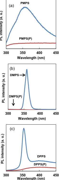
Photoluminescence spectra of PMPS, DMPS and DPPS thin films after
an-nealing are shown in Figure 7. The excitation wavelength was 250 nm. PMPS,
DMPS and DPPS exhibited photoluminescence with emission at 300 - 450 nm. Decreased photoluminescence intensities for PMPS, DMPS and DPPS were
ob-served upon doping, attributed to structural transition from the addition of PBr3
and annealing at 300˚C. This characteristic has been previously explained by
light-induced charge separation between polysilane units and P [17].
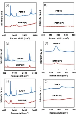
Raman scattering spectra of PMPS DMPS and DPPS thin films after annealing
are shown in Figure 8. Raman active modes of the PMPS(P) film were observed
at 1001, 1032, 1103, 1590, 2901, 2965 and 3053 cm−1. Peaks at 1001, 1032, 1103
and 1590 cm−1 in the spectrum of PMPS were attributed to phenyl group
vibra-tion modes. Peaks at 2901, 2965 and 3053 cm−1 in the spectrum of PMPS were
[image:9.595.312.436.326.701.2]attributed to methyl group vibration modes. Adding PBr3 to PMPS decreased the
Figure 7. Photoluminescence spectra of (a) PMPS, (b) DMPS and (c) DPPS thin films, with and without P doping.
300 350 400 450
P
L
i
n
te
n
s
ity
(a
. u
.)
Wavelength (nm)
300 350 400 450
P
L
i
n
te
n
s
ity
(a
. u
.)
Wavelength (nm)
300 350 400 450
P
L
i
n
te
n
s
ity
(a
. u
.)
Wavelength (nm)
DMPS
DMPS(P)
DPPS
DPPS(P) PMPS
PMPS(P) (a)
(b)
Figure 8. Raman scattering spectra of (a) and (d) PMPS, (b) and (e) DMPS and (c) and (f) DPPS thin films, with and without P doping.
peaks at 1001, 1590, 2901, 2965 and 3053 cm−1. Vibrations of the Si crystal lattice
at ca. 520 cm−1[18] were not observed in the spectra of the PMPS or PMPS(P)
thin films. A peak at 480 cm−1 was observed in the spectrum of the DMPS thin
film owing to amorphous Si [8], and its intensity decreased upon doping. No
peaks were apparent at 400 - 600 cm−1 in the spectrum of the DPPS thin film.
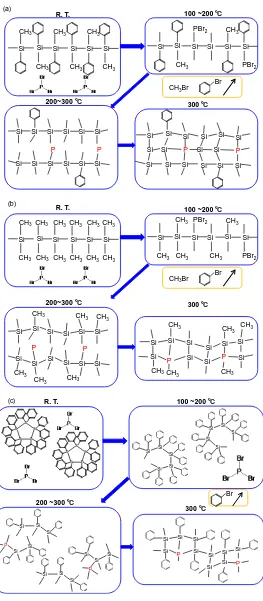
Proposed mechanisms for P doping in PMPS, DMPS and DPPS are shown in Figure 9. Phenyl and methyl groups in PMPS side chains desorbed during
an-nealing at 300˚C, and −PBr2 bound to PMPS side chains. Methyl bromide and
benzene bromide were formed, and an amorphous structure formed from the Si
chain structure [19]. Numerous methyl groups desorbed from DMPS side
chains, and −PBr2 bound to side chains during annealing. Methyl bromide was
formed, and an amorphous structure was formed from the main Si chain struc-ture. A Si ring opening reaction occurred in DPPS. Si-Si bonds were broken, and numerous phenyl groups also desorbed from DPPS side chains.
3.3. Photovoltaic Properties of Thin Films
Parameters measured for PMPS(P)/P3HT, DMPS(P)/P3HT and DPPS(P)/P3HT
400 1400 2400 3400
In
te
n
s
ity
( a
.u
.)
Raman shift (cm-1)
400 1400 2400 3400
In
te
n
s
ity
(a
. u
.)
Raman shift (cm-1)
400 1400 2400 3400
In
te
n
s
ity
(a
. u
.)
Raman shift (cm-1)
(a)
(b)
(c)
PMPS
PMPS(P)
DMPS
DMPS(P)
DPPS
DPPS(P)
400 450 500 550 600
In
te
n
s
ity
(a
. u
.)
Raman shift (cm-1)
400 450 500 550 600
In
te
n
s
ity
(a
. u
.)
Raman shift (cm-1)
(e)
(f)
400 450 500 550 600
In
te
n
s
it
y
(
a
.u
.)
Raman shift (cm-1) (d)
PMPS
PMPS(P)
DMPS
DMPS(P)
DPPS
Figure 9. Proposed changes in microstructure of (a) PMPS(P), (b) DMPS(P) and (c) DPPS(P) during annealing.
heterojunction solar cells are summarized in Table 4. The ITO/TiOx/PMPS(P)/
P3HT/PEDOT:PSS/Au solar cell generated a photocurrent and photovoltage,
Si Si Si CH3 CH3 CH3 Si Si CH3 CH3 Si CH3 PBr2
Si Si Si Si Si Si
CH3Br
Br
R. T.
CH3
CH3
PBr2
Si Si Si Si Si Si
Si Si Si Si Si Si
P P
Si Si Si Si Si Si
Si Si Si Si Si Si
P
Si Si Si Si P
100 ~200 ℃
200~300 ℃
300 ℃
(a)
Si Si Si CH3 CH3 CH3 Si Si CH3 CH3 Si CH3 PBr2
Si Si Si Si Si Si
CH3Br
Br
R. T.
CH3
CH3
PBr2
Si Si Si Si Si Si
Si
Si Si Si Si Si
P P Si
Si Si
Si Si Si Si
Si P
Si P Si
100 ~200 ℃
200~300 ℃ 300 ℃
CH3 CH3 CH3
CH3 CH3 CH3
CH3
CH3 CH3
(b)
CH3 CH
3
CH3
CH3 CH3
CH3
CH3 CH
3
CH3
CH3CH3 CH3
R. T. 100 ~200 ℃
300 ℃
Si Si Si Si Si
200 ~300 ℃
(c)
Br Si Si Si Si Si Si Si Si Si Si Si Si Si Si Si Si P Si Si Si Si Si Si Si Si P
Si Si Si
Si Si
P Si Si
Si
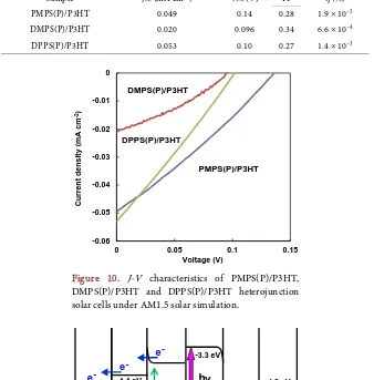
with an open-circuit voltage (VOC) of 0.14 V, short-circuit current (JSC) of 0.049
mA∙cm−2, fill factor (FF) of 0.21 and power conversion efficiency (η) of 1.9 ×
10−3%. These parameters were better than those exhibited by the other devices,
as shown in Figure 10. The photoresponse arose from photoinduced carriers
generated at P3HT layers. η is lower than values of ordinary organic solar cells, which is attributed to interfacial defects of the p-n junction. Further improve-ment of the interfacial structure is therefore necessary.
The energy level diagram of the PMPS(P)/P3HT heterojunction solar cell is
shown in Figure 11, in which reported values were used for energy levels [20]
[21]. P3HT generated the electronic carriers in the PMPS(P)/P3HT
[image:12.595.205.543.275.618.2]heterojunc-tion solar cell, which explained the increase in efficiency.
Table 4. Photovoltaic parameters of polysilane(P)/P3HT heterojunction solar cells. Sample JSC (mA∙cm−2) VOC (V) FF η (%)
PMPS(P)/P3HT 0.049 0.14 0.28 1.9 × 10⁻³
DMPS(P)/P3HT 0.020 0.096 0.34 6.6 × 10⁻⁴
DPPS(P)/P3HT 0.053 0.10 0.27 1.4 × 10⁻³
Figure 10. J-V characteristics of PMPS(P)/P3HT, DMPS(P)/P3HT and DPPS(P)/P3HT heterojunction solar cells under AM1.5 solar simulation.
Figure 11. Energy level diagram of the PMPS(P)/P3HT heterojunction solar cell.
-0.06 -0.05 -0.04 -0.03 -0.02 -0.01 0
0 0.05 0.1 0.15
C
u
rr
e
n
t d
e
n
s
ity
(
m
A
cm
-2)
Voltage (V)
DMPS(P)/P3HT
PMPS(P)/P3HT DPPS(P)/P3HT
PEDOT: PSS
-4.7 eV -4.4 eV
-5.2 eV
-4.8 eV
ITO PMPS(P) Au
-3.3 eV
P3HT
-8.1 eV
TiOx
-5.0 eV
h+ hν
e -e -e
[image:12.595.270.477.570.705.2]Energy barriers existed near the semiconductor/metal interface, and charge was transferred by light irradiation from the ITO substrate side. Holes were transported to the Au electrode and electrons to the ITO substrate. The present polysilane materials might also be utilized as hole transport materials for the
re-cent developed perovskite – based solar cells [22][23].
4. Conclusion
PMPS, DMPS and DPPS thin films were fabricated by spin-coating, and the ef-fect of doping with P was investigated. PMPS(P) thin films exhibited an amorphous structure after annealing at 300˚C, while DMPS(P) and DPPS(P) thin films were crystalline after annealing. Crystallite sizes of PMPS(P), DMPS(P) and DPPS(P) thin films were 6.9, 22 and 64 nm, respectively, and the polysilane films possessed nanoparticle structures. In the absence of light, PMPS(P) and DMPS(P) thin films exhibited decreased electrical resistances upon P doping. The energy gaps of PMPS, DMPS and DPPS were 3.3, 3.9 and 3.4 eV, respec-tively, and those of PMPS(P), DMPS(P) and DPPS(P) were 3.5, 3.9 and 3.8 eV, respectively. A decrease in photoluminescence intensity of all thin films was ob-served upon P doping, because of light-induced charge separation between poly-silane units and P. Annealing at 300˚C caused the desorption of phenyl and
me-thyl groups from PMPS(P) side chains. A peak at 480 cm−1 was observed in the
Raman spectrum of the DMPS thin film. This arose from amorphous Si, and de-creased in intensity upon P doping. Thus, P was doped in polysilanes, and PMPS acted as an n-type semiconductor. Solar cells with PMPS(P)/P3HT, DMPS(P)/ P3HT and DPPS(P)/P3HT heterojunction structures were fabricated and exhi-bited photovoltaic behavior.
Acknowledgements
This work was partly supported by Satellite Cluster Program of the Japan Science and Technology Agency, and a Grant-in-Aid for Scientific Research (C) No. 25420760.
References
[1] Lee, J., Seoul, C., Park, J. and York, J. (2004) Fullerene/poly(methylphenylsilane) (PMPS) Organic Photovoltaic Cells. Synthetic Metals, 145, 11-14.
https://doi.org/10.1016/j.synthmet.2004.04.022
[2] Silence, S., Scott, J., Hache, F., Ginsbrug, E., Jenkner, P., Miller, P., Twieg, R. and Moermer, W. (1993) Poly(silane)-Based High-Mobility Photorefractive Polymers.
Journal of the Optical Society of America B, 10, 2306-2312.
https://doi.org/10.1364/josab.10.002306
[3] Jung, J., Ciesielski, W. and Ulanski, J. (2006) Photovoltaic Effect in Novel Polysilane with Phenothiazine Rings and Its Blends with Fullerene. Materials Science-Poland, 24, 527-534.
[4] Masuda, T., Matsuki, Y. and Simoda, T. (2012) Stability of Polydihydrosilane Liquid Films on Solid Substrates. Thin Solid Films, 520, 5091-5096.
[5] Masuda, T., Matsuki, Y. and Simoda, T. (2012) Pyrolytic Transformation from Po-lydihydrosilane to Hydrogenated Amorphous Silicon Film. Thin Solid Films, 520, 6603-6607. https://doi.org/10.1016/j.tsf.2012.07.028
[6] Masuda, T., Matsuki, Y. and Simoda, T. (2009) Spectral Parameters and hamaker Constants of Silicon Hydride Compounds and Organic Solvents. Journal of Colloid and Interface Science, 340, 298-305. https://doi.org/10.1016/j.jcis.2009.08.028
[7] Iyer, G.R.S., Hobbie, E.K., Guruvenket, S., Hoey, J.M., Anderson, K.J., Lovaasen, J., Gette, C., Schulz, D.L., Swenson, O.F., Elangovan, A. and Boudjouk, P. (2012) Solu-tion-Based Synthesis of Crystalline Silicon from Liquid Silane through Laser and Chemical Annealing. Applied Materials and Interfaces, 4, 2680-2685.
https://doi.org/10.1021/am300334p
[8] Shimoda, T., Matsuki, Y., Furusawa, M., Aoki, T., Yudasaka, I., Tanaka, H., Iwasaki, H., Wang, D., Miyasaka, M. and Takeuchi, Y. (2006) Solution-Processed Silicon Films and Transistors. Nature, 440, 783-786. https://doi.org/10.1038/nature04613
[9] Nakagawa, J., Oku, T., Suzuki, A., Akiyama, T., Tokumitsu, K., Yamada, M. and Nakamura, N. (2012) Fabrication and Characterization of Polysilane/C60 Thin Film
Solar Cells. Journal of Physics Conference Series, 352, 012019-1-5.
https://doi.org/10.1088/1742-6596/352/1/012019
[10] Kawashima, A., Oku, T., Suzuki, A., Kikuchi, K. and Kikuchi, S. (2012) Microstruc-tures and Photovoltaic Properties of Polysilane/C60-Based Solar Cells. Materials Science and Applications, 3, 557-561. https://doi.org/10.4236/msa.2012.38079
[11] Masuda, T., Sotani, N., Hamada, H., Matsuki, Y. and Simoda, T. (2012) Fabrication of Solution-Processed Hydrogenated Amorphous Silicon Single-Junction Solar Cells.
Applied Physics Letters, 100, Article ID: 253908. https://doi.org/10.1063/1.4730614
[12] Oku, T., Nakagawa, J., Iwase, M., Kawashima, A., Yoshida, K., Suzuki, A., Akiyama, T., Tokumitsu, K., Yamada, M. and Nakamura, M. (2013) Microstructures and Photovoltaic Properties of Polysilane-Based Solar Cells. Japanese Journal of Applied Physics, 52, Article ID: 04CR07. https://doi.org/10.7567/jjap.52.04cr07
[13] Martin, P.H., Irmer, G. and Muller, E. (1998) Submicro Structure of Silicon Carbide Derived from Poly(Methylchlorosilane). Journal of the European Ceramic Society, 18, 193-199. https://doi.org/10.1016/S0955-2219(97)00125-8
[14] Boo, B.H. (2011) Infrared and Raman Spectroscopic Studies Tris (Trimethylsilyl) Silanederivatives of (CF3)(3) Si)(3) Si−X [X = H, Cl, OH, CH3, OCH3, Si(CH3)(3)]:
Vibrational Assignments by Hartree-Fock and Density-Functional Theory Calcula-tions. Journal of the Korean Physical Society, 59, 3192-3200.
[15] Boo, B.H. (2011) Infrared and Ramanspectroscopy of Diphenylsilane. Vibrational Assignment by Hartree-Fock and Density-Functional Theory Calculations. Journal of the Korean Physical Society, 59, 3205-3209. https://doi.org/10.3938/jkps.59.3205
[16] Kidowaki, H., Oku, T. and Akiyama, T. (2012) Fabrication and Evaluation of CuO/ZnO Heterostructures for Photoelectric Conversion. International Journal of Research and Reviews in Applied Sciences, 13, 67-72.
[17] Tanaka, H., Iwasawa, H., Wang, D., Toyoda, N., Aoki, T., Yudasaka, I., Matsuki, Y., Shimoda, T. and Furusawa, M. (2007) Spin-on N-Type Silicon Films Using Phos-phorous-Doped Polysilanes. Japanese Journal of Applied Physics, 46, L886-L888.
https://doi.org/10.1143/JJAP.46.L886
[18] De Wolf, I. (2003) Raman Spectroscopy: About Chips and Stress. Spectroscopy Eu-rope, 15, 6-13.
[20] Oku, T., Takeda, A., Nagata, A., Kidowaki, H., Kumada, K., Fujimoto, K., Suzuki, A., Akiyama, T., Yamasaki, Y. and Ōsawa E. (2013) Microstructures and Photovol-taic Properties of C60-Based Solar Cells with Copper Oxides, CuInS2,
Phthalocya-nines, Porphyrin, PVK, Nanodiamond, Germanium and Exciton-Diffusion Block-ing Layers. Materials Technology, 28, 21-39.
https://doi.org/10.1179/1753555712Y.0000000042
[21] Jin, Y.K., Sun, H.K., Hyun, H.L., Kwanghee, L., Wanli, M., Xiong, G. and Alan, J.H. (2006) New Architecture for High-Efficiency Polymer Photovoltaic Cells Using So-lution-Based Titanium Oxide as an Optical Spacer. Advanced Materials, 18, 572- 576. https://doi.org/10.1002/adma.200501825
[22] Oku T., Ohishi Y., Suzuki A. and Miyazawa Y. (2016) Effects of Cl Addition to Sb-Doped Perovskite-Type CH3NH3PbI3 Photovoltaic Devices. Metals, 6, 147. https://doi.org/10.3390/met6070147
[23] Shirahata, Y., Yamomoto, Y., Suzuki, A., Oku, T., Fukunishi, S. and Kohno, K. (2017) Effects of Polysilane-Doped Spiro-OMeTAD Hole Transport Layers on Photovoltaic Properties. Physica Status Solidi A, in press.
https://doi.org/10.1002/pssa.201600591
Submit or recommend next manuscript to SCIRP and we will provide best service for you:
Accepting pre-submission inquiries through Email, Facebook, LinkedIn, Twitter, etc. A wide selection of journals (inclusive of 9 subjects, more than 200 journals)
Providing 24-hour high-quality service User-friendly online submission system Fair and swift peer-review system
Efficient typesetting and proofreading procedure
Display of the result of downloads and visits, as well as the number of cited articles Maximum dissemination of your research work
Submit your manuscript at: http://papersubmission.scirp.org/