VLSI DESIGN OF EFFICIENT ARCHITECTURE IN
RECURSIVE PSEUDO-EXHAUSTIVE TWO-PATTERN
GENERATION
1G. SUDHAGAR, 2 Dr. S. SENTHIL KUMAR
1Asst Prof., Department of Electronics and Communication Engineering,
Sri Venkateswara College of Engineering and Technology, Thiruvallur.
2
Assoc. Prof., Department of Electrical Engineering, GCE, Salem.
E-mail: [email protected], [email protected]
ABSTRACT
The aim of built in self-test is to make the machine to test by itself. The best method among the built in self-test is pseudo exhaustive two pattern generation produces the output according to the input given with 16bit generator. The main drawback that occurs in this test pattern generation is maximum delay. It occurs in the carry generator module. In this paper, the method proposed with recursive pseudo exhaustive two pattern generator to reduce the delay is that mixing the block of carry generator and adder in order to minimize the delay that produced while in testing process. A method of approaching the testing problem at the chip level is to appropriate built-in self-test capacity that present inside a chip. In exhaustive testing number of test vector are more which is decreased in pseudo exhaustive testing. Built in self-Test pattern generators are commonly discerned into one-pattern and two-pattern generators.
Keywords: Built In Self-Test, Two Test Pattern Generator, Carry Generator, Recursive, And
Pseudo-Exhaustive Generator.
1. INTRODUCTION
The motivation of testing a integrated chip to predict its functionality is extremely complex and it is frequently time consuming process. A method of approaching the testing problem at the chip level is to appropriate built-in self-test capacity that present inside a chip [1]. Built in self-test is more suitable for periodic testing which is carried out periodically in the system itself [2]. This can be either on-line or off-line. Built in self-test consists of TPG, response analyzer and testing logic. In Built in self-test process, designing of TPG is very complex. Normally, Linear Feedback Shift Registers is widely used TPG in Built in self-test structure [3]. Even though it is suitable for built in self-test, it has many drawbacks. It is a random pattern generator, which is hard in designing; it produces unnecessary patterns which improves the switching activity of the Carry lookup Table that leads to improves in testing period [4]. Because of these reasons exhaustive and pseudo exhaustive testing process are preferred [5]. In exhaustive testing number of test vector are more which is decreased in pseudo exhaustive testing. Built in self-Test pattern generators are commonly discerned into one-pattern and two-pattern generators. One-pattern generators are used to find combinational faults. It has been concluded that so
many mechanisms get failed in CMOS circuits that could not be designed by the stuck-at faults. Then, the digital circuits should operate at their highest possible speeds to improve their performance [6].For correct behavior of the circuits, delay faults are found out by two pattern test generators [7]. In Built in Self-Test, the test pattern generation and the output response evaluation are done on chip itself so the hardware used for designing BIST should be minimized.
1.1 Methods Of Testing
There are several methods such as
and generic pseudo exhaustive two pattern generator (GPET) needs minimum hardware utilization. RPET needs 18n in addition to 8m gates and GPET also needs 16n gates [11]. Two Test pattern generator (TPGs) are designed and GPET is used for the built in self-testing process [12]. It produces all the tests for any cone size (k). By using this GPET more than a circuit is tested in parallel which improves the speed of the Built in self-test [13] . In this method 2 circuits like Wallace tree multiplier and 7-bit cryptographic circuit are tested in parallel [14]. The outputs from circuits are compared with the stored values and faults are determined [15].
1.2 Built In Self-Test
The Built in self-test is a mechanism that permits machine to test by its own. It is designed mainly for testing technique, as it made the electrical testing of a chip very easy, fast, more efficient, and less cost compare to other techniques. It is also the best answer to the testing of complex circuits that have no direct connections to external pins, such as memories present in embedded circuits which is used by the devices internally. It also suitable for on-chip test generation and response verification. The Advantages of implementing this method includes: 1) low cost of test, 2) better fault coverage, 3) minimal test time.
Exhaustive and pseudo-exhaustive test pattern generators give high failure coverage with reduced number of test patterns and without failure coverage simulation. Pseudo-exhaustive testing removes the need of deterministic test pattern generation. In this case, the pseudo-exhaustive the objective can be again formulated in such way that the n-bit gap is closed as if for sharing k-bit subspaces, every one of the 2k patterns generates at least once.
Recently modern VLSI circuits, that contains millions of transistors with the usage of same Built in self-test pattern generator to find at least one module which reduces the cost less among all modules in circuits. This pattern generator divided into one-pattern generator and two-pattern generator. One-pattern generator finds the stuck-at faults in the combinational circuits. The two-pattern test is used to find sequential faults such as stuck-open faults in CMOS circuits. It is also used to test the circuits at maximum speeds and also testing for the correct behavior that related to the material, it is known as delay testing.
A generic pseudo exhaustive two-pattern generator generates an (n,k) – pseudo exhaustive two-pattern test for any value of k, by enabling an input signal P[k], 1 ≤ k ≤ n. The generic pseudo-exhaustive two-pattern generator can be categorized
into progressive two-pattern generator that produces all (n,k)-pseudo-exhaustive two-pattern test vectors for all values of k. This technique is called as recursive pseudo exhaustive two-pattern generation. In recursive pseudo-exhaustive testing, (n,k)-PETS are generated for all k= 1,2,3,…..,n. With the usage of an array of Exclusive OR gates and binary counter can easily repeatedly produce all (n,k) pseudo-exhaustive test patterns for k ≤ n in reduced time.
1.3 Pseudo –Exhaustive Test Pattern Generation
Pseudo-exhaustive test pattern generators provide for complete failure coverage that does not need for failure simulation. In pseudo-exhaustive less number of test patterns are used. The Testing process in some types of systems, such as digital signal processor systems, memories present in embedded system and other, includes division of the inputs into nearby groups. Pseudo-exhaustive two pattern generator is a block with n inputs P [n:1] and n outputs A[n:1] that can produce a two-pattern (n,k)-pseudo-exhaustive test set for any value of k, (k ≤ n). The proposed generic pseudo-exhaustive two-pattern generator has n-stage generic counter; an n-stage accumulator that consists of adder, internal register, carries generator and a logic control. In method of two pattern generators like Generic pseudo exhaustive two pattern generator and recursive pseudo exhaustive two pattern generator are created to produce two pattern generator tests for circuits that have variety of shapes in cone manner. The generic pseudo-exhaustive two-pattern generator is presented and consists of a generic counter, one’s complement adder, a controller and a carry generator. The pattern with seven bit circuit design PE [7:1] is given as an input to the controller, generic counter, carry generator and the output A [7:1] is taken from the Accumulator.
accumulator-multiplier is available and b) since a multiplier-adder or multiplier-accumulator is suitable for test pattern generation, these schemes have improved power and energy consumption during testing. Recently it was known that an accumulator can be changed to function, in test mode, as a Non-Linear Feedback Shift Register (NLFSR) and that it can be produced.
Efficient for test output compression. In this implementation we propose that an accumulator functioning as a NLFSR can also be suitable as a bit-serial test pattern generator achieving the same failure coverage with the schemes of test vectors. Furthermore, the usages of the proposed scheme is larger, since, in opposite to the methods proposed ,it does not need the Usability of a multiplier in the operational circuit. The remaining of the paper is functioned as follows. It brings to bit serial test pattern generation methods based on arithmetic units. In this proposed methods new accumulator-based bit serial test pattern generation method, while on experimental results in order to makes scheme to be measured and compared with the already known bit-serial test pattern generation methods.
2. RESEARCH METHODOLOGY
The proposed method that uses in this
paper is combining the block of adder and carry generator in order to reduce the delay that occurs due to carry generator. The proposed block diagram is shown in figure 2.1
end_k_bit_test PE[n-1] n C_reset C_clk_dis C[n:1] A_reset0 A_resetN-1
Reset A[n:1]
[image:3.612.304.527.218.626.2]
Figure 2.1: Generic Pseudo-Exhaustive Two – Pattern Generator.
2.1 Counter Circuit
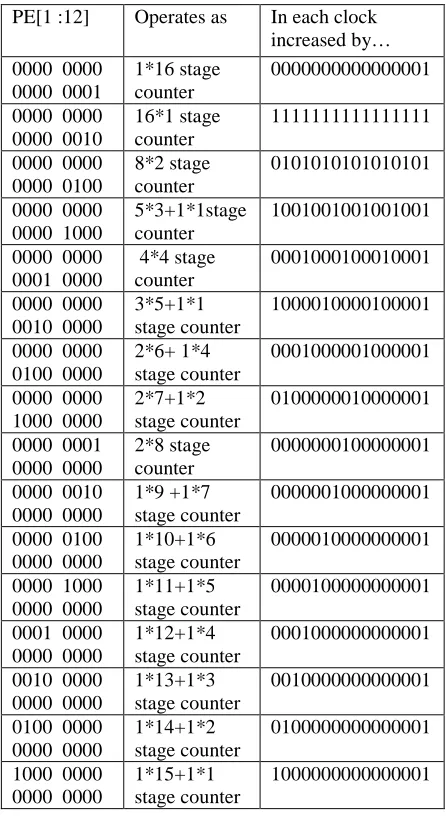
The n-stage generic counter get inputs a basic clock signal(clk) and n signals PE[n:1] ,if all signals PE[i],where 1≤i≤n are disabled, then the generic counter starts operated as an n-stage binary counter. The same makes true in PE[1]=1.When PE[k] is enabled ,for some value of k,1≤k≤n, every stages as k,2k,3k etc. ..Are clocked by the basic clock signal
Table I: Generic -Pseudo Exhaustive Generator
Therefore, the generic counter produces all 2k-1*(2k-1-1) groups to all groups of k-1 adjacent bits i.e., works as [n/(k-1)] consecutive k-stage counters. When C_clk_disable is activated, the clk signal is deactivated, and the generic counter remains idle .In figure 2.2 we propose the operation of a 16-stage generic counter for the various values of the PE[i] signals. From the function of the PE[1 :12] Operates as In each clock
increased by… 0000 0000
0000 0001
1*16 stage counter
0000000000000001
0000 0000 0000 0010
16*1 stage counter
1111111111111111
0000 0000 0000 0100
8*2 stage counter
0101010101010101
0000 0000 0000 1000
5*3+1*1stage counter
1001001001001001
0000 0000 0001 0000
4*4 stage counter
0001000100010001
0000 0000 0010 0000
3*5+1*1 stage counter
1000010000100001
0000 0000 0100 0000
2*6+ 1*4 stage counter
0001000001000001
0000 0000 1000 0000
2*7+1*2 stage counter
0100000010000001
0000 0001 0000 0000
2*8 stage counter
0000000100000001
0000 0010 0000 0000
1*9 +1*7 stage counter
0000001000000001
0000 0100 0000 0000
1*10+1*6 stage counter
0000010000000001
0000 1000 0000 0000
1*11+1*5 stage counter
0000100000000001
0001 0000 0000 0000
1*12+1*4 stage counter
0001000000000001
0010 0000 0000 0000
1*13+1*3 stage counter
0010000000000001
0100 0000 0000 0000
1*14+1*2 stage counter
0100000000000001
1000 0000 0000 0000
1*15+1*1 stage counter
1000000000000001
Control
Generic
Counte
Adder and C_gen
[image:3.612.63.290.385.667.2]generic counter we can see that it can create either one pattern exhaustive test set (when PE[1] is enabled), or one pattern (n,k) pseudo-exhaustive test set when PE[k+1] is activated.
A 16-stage generic counter is proposed in above figure2.2. It comprises of 16 generic counter cells (GCC) and an OR gates. The GCC is a changed version of the typical counter cell and is implementation for the case ripple counter designs can be found. If Seli is activated, the stage I of the
counter is clocked by the basic clock signal. Thus, Seli is activated if and only if i is a multiple of k.
Therefore, the select signal of every stage i is the output of an OR gate, whose inputs are the signals PEj, for all j that divide i. If I is a prime number (is
divided only by 1) there is no need for an OR gate, and the select signal is driven by the signal PEi, For
instance, the OR group of gates of a 16 stage generic counter is presented in table.
2.2 Control Block
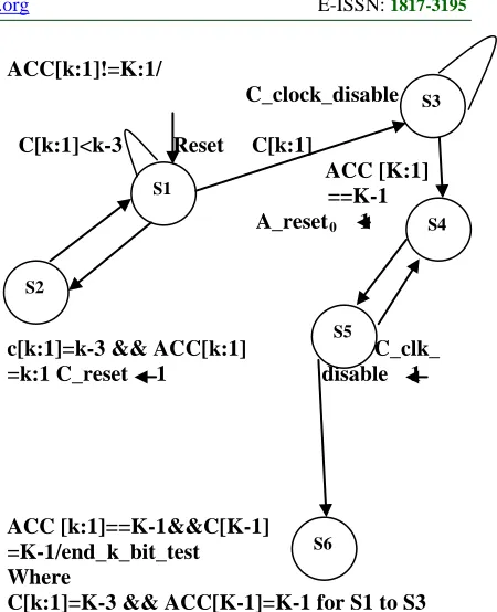
The purpose of the control module is to say
that a k-stage two pattern test is created at the k low order stages of the generator. If this is complete, the following the above reasoning,(n-k) pseudo-exhaustive test is generated. The operation of the control module is depends on the algorithm proposed. The ACC structure performs the accumulation function with one’s complement addition. Thus, the test pattern generator algorithm tests the function of an accumulator whose inputs are lead by a binary counter. The counter counts from 1 to K-3(phase1, steps 3-5) and then it is restart, this is again until the outputs of the counter are equal to K-3 and the outputs of the accumulator are equal to K-1.The counter is increased to K-2 and the accumulator recursively accumulates K-2 until its outputs is equal to K-1.Finally all transitions to and from zero are produced by keeping the accumulator and increasing the counter each second clock cycle.
In the test pattern generator algorithm was concluded to produce all n-bit 2 pattern tests within 2k*2k-1+ 1 clock cycles, i.e. within the theoretically reduced time. The function of the test pattern algorithm for k=3 stages is demonstrated. The control module takes inputs the signals C_clkdisable,C_reset,A_reset0,end_k_bit_test.It
works as gives C[K:1] denotes the k low order stages of the counter module, while ACC[k:1] decides the k low –order stages of the accumulator. When C%K ==K-3 i.e ,C[k:1] = K-3, the generic counter is reset in the next cycle phase the test pattern algorithm.
ACC[k:1]!=K:1/
C_clock_disable 1 C[k:1]<k-3 Reset C[k:1]
ACC [K:1]
==K-1 A_reset0 1
c[k:1]=k-3 && ACC[k:1] C_clk_ =k:1 C_reset 1 disable 1
ACC [k:1]==K-1&&C[K-1] =K-1/end_k_bit_test Where
[image:4.612.310.535.80.357.2]C[k:1]=K-3 && ACC[K-1]=K-1 for S1 to S3
Figure 2.3: State Diagram Of The Operation Of The Control Module.
When C%K == K-3 i.e., C[k:1] = K-3 and ACC%K == K-1 i.e., ACC[k:1] = K-1 the counter is counted again and the counter clock is deactivated from the following cycle. When ACC %k == K-1, then the 3rd phase of the pattern generator algorithm said , during which the clock of the particular counter is lead by the divided by two clock signal and the accumulator is restart to zero every second clock cycle. When both the accumulator and the generic counter attain the value K-1, the end _k_bit_test signal is activated, to denote the end of the (n.k) pseudo-exhaustive test. The detect module is a sequence of OR-AND gates that find the occurrence of certain values at the outputs of the A[n:1],C[n:1] and PE[n:1] buses. An implementation of the findable module is proposed for the case n=16 .The signal AN-1is calculated
instead of the signal AK-1.The two signals are equal
since when A[k:1] = K-1 , then the k low order outputs of the accumulator are equal to 1,thus all outputs of the accumulator are equal to 1.The implementation of AK-1,since the former needs less
hardware overhead n gates instead 2n gates needed for the evaluation of AK-1.
For instance Given that PE[i]=0 for all i≠n, the shaded AND gates are disabled ,therefore only C[n:1] and A[n:1] affect the values of the signals Ck-n,Ck-(n-1),etc. detect the values of the signal
values. Signal AN-1=AK-1 is an n – input AND gate.
S2
S6 S5
S4 S3
2.3 Adder And Carry Generator Circuit
The inputs of adder are cin, A[16:1], C[16:1]
and its outputs are C_out[16:1], A[16:1]. It comprises of stages of full adders, the carry output of the full adders are lead to the next full adders as carry input. If the value of k is considered to be 3 then the accumulator works as two 3-stage sub accumulator and one 1-stage accumulator. The carry output of each sub accumulator is provided to the carry input of next sub accumulator. If there is any carry in the 3rd bit then it is added to the lowest order bit of the adder output.
The carry output of each sub accumulator is providing to the carry input of next sub accumulator. If there is any carry in the third bit then it is added to the lowest order bit of the adder output. It provides one bit addition and output saves in internal register. For n-stage operation carry is created by carry generator. The adder takes the input from the counter, and then Count is giving to the carry generator. When the clock signal is activated adder functions one bit addition. The internal register is having capacity of saving output of the adder. The adder is setting the values again by reset A signal and the register is also setting again by individual reset signal. The input clock signal is deactivated the adder remains idle.
3. LITERATURE REVIEW
A Built-in self-test (BIST) technique based on pseudo-exhaustive testing is proposed in this paper. Two pattern test generator is used to provide high fault coverage. Testing for delay and sequential faults needs pattern tests. In two-pattern testing method all possible group of the test vectors are given to the circuit which is kept under test. In this method a pseudo exhaustive two-pattern generator with fewer hardware that produces two-pattern (7,k)-adjacent bit pseudo exhaustive tests for any k<7 is used. The 2 circuits like Wallace tree multiplier and cryptographic circuit that based on RSA algorithm are tested in parallel. The main merit of this Built In Self-Test is that the circuits have different cone sizes are tested at a time. It improves the speed of this test.
Pseudo-exhaustive testing involves getting all combination of input test patterns to the each and the corresponding output with the shape of cones to test the features of a combinational circuit. It gives high failure coverage of findable combinational failure with reduced number of test patterns than the ideal exhaustive test pattern generation. In (n,k)-adjacent bit pseudo-exhaustive test sets, all 2k binary groups appear to all adjacent k-bit of input
groups. With repeated pseudo-exhaustive generation, all (n,k) adjacent bit pseudo-exhaustive test patterns are created for k ≤ n and more than one modules can be tested in parallel. The two pattern test is used to find series failures such as stuck-open faults in CMOS circuits. Delay testing is also used to detect correct circuit operation at regular clock speeds needs two pattern testing. Here pseudo exhaustive two pattern generator is presented and all (n,k) adjacent bit pseudo exhaustive tests are generated for k ≤ n recursively.
The test on the level of wafer during in is a general technique to minimize test and burn-in costs burn-in semiconductor manufacturburn-ing. However, scan-based testing leads to important power changes in a die during test-pattern application. This change completely affects the accuracy of predictions of temperatures produced in the junction and the speed needed for burn-in. A test-pattern ordering technique aims to reduce the changes in power consumption during test application. The issues based on test-pattern ordering are formulated and that has been cleared accurately using integer linear optimization. Efficient heuristic methods are also required to easily solve the pattern-ordering problem for large circuits. The results from simulation are here for the standard circuits, and the proposed ordering technique based on 3rd baseline is compared with 2nd baseline methods that bring out pattern ordering to reduce peak power and average power, respectively. The baseline method that randomly makes test patterns to measure the methods that are proposing.
The volume of VLSI circuits increases, it becomes more impressed to integrate dedicated test logic on a chip. This Built-in Self-Test (BIST) method not only produces financial advantages but also efficient technical needs with respect to categorized testing and the reuse of test logic during the application of the circuit. Begins with a whole on test problems, test applications and terms used in this survey views general test methods and analyzes the basic test procedure. The method of BIST is generated and discussed, BIST concepts for random logic as well as for structured logic are shown.
that consists of electronic components and systems. It is therefore not to but also that the testing as a key technology component with significant importance. This method provides common test methods and creates the concept of Built-in Self-Test (BIST) as an efficient approach to overcome the drawbacks of the common test technology that become more and more conspicuous. It provides the specific techniques for BIST of structured logic.
4. RESULTS AND DISCUSSIONS
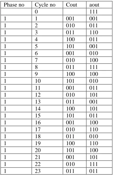
[image:6.612.89.290.423.726.2]Built In Self-Test techniques generally mixes a built-in binary pattern generator with circuitry for grouping the related response data generated by the circuit under test. The compressed form of the output data is compared with a known failure free response. Built-in Self-Test plays a significant role in recent VLSI technology. The Built in self-test should occupy reduced area for compressed design of digital circuit. When compared to the results of the test pattern generator proposed in need of lesser hardware to implement. Depends on the technique used in a test pattern is produced. The comparison of the hardware overall circuit is shown in table.
Table II: Two Pattern Generated By Test Pattern Generator
Phase no Cycle no Cout aout
0 111
1 1 001 001 1 2 010 011 1 3 011 110 1 4 100 011 1 5 101 001 1 6 001 010 1 7 010 100 1 8 011 111 1 9 100 100 1 10 101 010 1 11 001 011 1 12 010 101 1 13 011 001 1 14 100 101 1 15 101 011 1 16 001 100 1 17 010 110 1 18 011 010 1 19 100 110 1 20 101 100 1 21 001 101 1 22 010 111 1 23 011 011
1 24 100 111 1 25 101 101 1 26 001 110 1 27 010 001 1 28 011 100 1 29 100 001 1 30 101 110 1 31 001 111 1 32 010 010 1 33 011 101 1 34 100 010 1 35 101 111 2 36 110 110 2 37 110 101 2 38 110 100 2 39 110 011 2 40 110 010 2 41 110 001 2 42 110 111 3 43 001 000 3 44 001 001 3 45 010 000 3 46 010 010 3 47 011 000 3 48 011 011 3 49 100 000 3 50 100 100 3 51 101 000 3 52 101 101 3 53 110 000 3 54 110 110 3 55 111 000 3 56 111 111
A lot of evaluations were done in order to measure the quality of the test sequences produced by our scheme. In the first set of our experiments we used the non-redundant version of the standard circuits while in the second set we propose results of the failure coverage are retained using the standard. For both circuits sets we think that the first inputs and the internal flip-flops are joined to a single scan chain. The failure coverage in each case was measured as the fraction of the number of failures found by the test vectors of the test pattern generator over the total number of easily findable failures. In each case, the numbers of clock cycles that are used to create and shift-in a new test vector were chosen to be relatively prime to the period of the produced sequence, in order to guarantee that highest number of variety of patterns can be given to the table
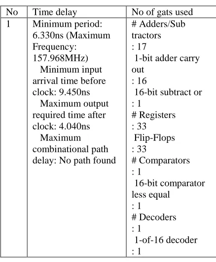
Table III: Output Result With Time Delay And Number Of Gates Required.
No Time delay No of gats used 1 Minimum period:
6.330ns (Maximum Frequency:
157.968MHz) Minimum input arrival time before clock: 9.450ns Maximum output required time after clock: 4.040ns Maximum combinational path delay: No path found
# Adders/Sub
tractors : 17
1-bit adder carry out : 16
16-bit subtract or : 1
# Registers : 33
Flip-Flops : 33
# Comparators : 1
16-bit comparator less equal : 1
# Decoders : 1
1-of-16 decoder : 1
Thus the n bit stage is done and output is
tabulated. The 7-bit stage is implemented for instance he time delay is reduced and its maximum value is given in above table and the number of gates are also mentioned.
Figure 4.3 Simulated Output for Pattern Generator
5. CONCLUSION
Pseudo-exhaustive test pattern generators provide very high failure coverage without the need for fault simulation or concluded test pattern generation for combinational faults. Nearby bit
pseudo-exhaustive testing is mainly aimed to data path structures that have a strongly bit organized character and contain internal buses that are divided into physically adjacent lines. In modern VLSI circuits consists millions of transistors, the use of the same Built in self-test pattern generator for finding more than one modules that can make lead down the hardware overhead, increasing the applicability of the BIST concept .Modules whose inputs are given during Built in self-testing from the same pattern generator may have different cone sizes. Recursive pseudo-exhaustive testing has been proposed as a answer to the issue in recursive and generic pseudo-exhaustive generators for the detection of struck-at faults have been proposed. On the contrary, no recursive pseudo-exhaustive two pattern generator has been presented to date. In this paper we have proposed a two pattern generator scheme that can generate generic and recursive pseudo-exhaustive test with this scheme, more than one circuit under test, possibly having different cone sizes can be tested in parallel. Thus the 16bit generator can be sampled and tested. It is then reduced the delay that occurs in carry generator block with the help of combining the adder circuit and carry generator in single block.
REFERENCES
[1] P. Bardell, W. McAnney, J. Savir, Built-in Test for VLSI, Pseudorandom Techniques. John Wiley & Sons, New York 1987.
[2] X. Sun, M. Serra, "Merging Concurrent Checking and Off-line BIST", Proc. International Test Conference 1992, Sept. 20-24 1992, Baltimore, MD, IEEE CS Press, pp. 958-967.
[3] R. Bennetts, Design of Testable Logic Circuits, Addison Wesley 1984.
[4] S. Gupta, D. Pradhan, "Can concurrent Checkers help BIST?", Proc. International Test Conference 1992, Sept. 20- 24 1992, Baltimore, MD, IEEE CS Press, pp. 140-150. [5] E. Amerasekera, F. Najm, Failure Mechanisms
in Semiconductor Devices, 2nd edition, John Wiley & Sons, Chichester 1997.
[6] Siemens, "Fourth Generation 16M-Bit DRAMs – Accelerated Soft Error Sensitivity", Information Note 5.96.
[7] V. Agrawal, C. Kime, K. Saluja, "A Tutorial on Built-In Self-Test", IEEE Design & Test of Computers, March 1993, pp. 73-80 and June 1993, pp. 69-77, IEEE CS Press.
[image:7.612.89.300.461.631.2]we need?", Proc. International Test Conference 1992, Sept. 20-24 1992, Baltimore, MD, IEEE CS Press, pp. 168-177. [9] C. Chen, S. Gupta, "BIST Test Pattern
Generators for Two-Pattern Testing – Theory and Design Algorithms", IEEE Transactions on Computers, vol. 45, no. 3, 1996, pp. 257-269.
[10] A. van de Goor, Testing Semiconductor Memories, Theory and Practice. John Wiley & Sons, Chichester 1991.
[11] B. Könemann et al., "Delay Test: The Next Frontier for LSSD Test Systems", Proc. International Test Conference 1992, Sept. 20-24 1992, Baltimore, MD, IEEE CS Press, pp. 578-587.
[12] E. McCluskey, "Built-In Self-Test Techniques", IEEE Design & Test of Computers, April 1985, IEEE CS Press, pp. 21-36.
[13] R.Fritzemeier, H. Nagle, C. Hawkins, "Fundamentals of Testability – A Tutorial", IEEE Transactions on Industrial Electronics, vol. 36, no.2, May 1989, pp. 117-128.
[14] J. Grason, "TMEAS, A Testability Measurement Program", Proc. 16th Design Automation Conference, San Diego, CS, June 1979, pp. 156-161.