Energy Efficient Implementation for Arithmetic
Application in CMOS Full Adders
T.Thirumurugan
1J.Sathish Kumar
2Professor, Dr.SJS PMCET 1 SET, Surya Group of Institutions2
ABSTRACT
The overall view of this paper is to attain high speed, low power full adder cells with alternative logic cells that lead to have reduced power delay product. Two high-speed and low-power full adder cells designed with an alternative internal logic structure and pass-transistor logic styles that lead to have a reduced power-delay product (PDP). We carried out a comparison against other full-adders reported as having a low PDP, in terms of speed, power consumption and area. All the full-adders were designed with a 0.18- m CMOS technology, and were tested using a comprehensive test bench that allowed to measure the current taken from the full adder inputs, besides the current provided from the power supply. Post-layout simulations show that the proposed full adders outperform its counterparts exhibiting an average PDP advantage of 80%, with only 40% of relative area. Adder module is the core of many arithmetic operations such as addition, subtraction, multiplication and division with an alternative internal logic structure based on the multiplexing of the Boolean function. To determine the lowest power supply voltage of full adders can tolerate by its correct functionality. Delay in full adder relates the amount of energy spent during the realization of the determined task. The design of the full adder circuit in Micro wind tool that allow measuring the Delay, Area, Power Consumption and Speed.
General Terms
Complementary Metal Oxide Semiconductor, Device under Test, Differential Cascade Voltage Switch, Swing Restored, Power Delay Product
Keywords
Arithmetic operations, delay, high speed, low power, Double Pass –transistor Logic, Complementary Pass-transistor Logic
1. INTRODUCTION
Energy Efficiency is one of the most required features for recent electronic systems designed for high-performance and small applications. In other hand, the ever increasing market segment of small electronic devices demands the availability of low-power building blocks that enable the implementation of long-lasting battery-operated systems. The general trend of increasing operating frequencies and circuit complexity, in order to cope with the throughput needed in modern high-performance processing applications, requires the design of very high-speed circuits using Micro wind tool.
The power delay product (PDP) relates the amount of energy spent during the realization for a particular task, and this is the important stands as the more fair performance metric when comparing optimizations of a module designed and tested using different technologies, operating frequencies, and scenarios. Addition is a fundamental arithmetic operation that is broadly used in many VLSI systems, such as application
specific digital signal processing (DSP) architectures and microprocessors. This module is the core of many arithmetic operations such as addition/subtraction, multiplication, division and address generation. As stated above, the PDP exhibited by the full-adder would affect the system’s overall performance [1]. Thus, taking this into consideration, the design of a full-adder having low-power consumption and low propagation delay results of great interest for the implementation of modern digital systems. In this paper, the report to design and performance comparison of two full-adder cells implemented with an alternative internal logic structure, based on the multiplexing of the Boolean functions XOR/ XNOR and AND/OR, to obtain balanced delays in SUM and CARRY outputs, respectively, and pass-transistor When compared with other ones reported previously low-power arithmetic modules.
This paper is organized as follows. The internal logic structure adopted as standard in previous papers for designing a full-adder cell and the alternative internal logic structure and the pass-transistor powerless/groundless logic styles used to build the two proposed full-adders.
1.1 Gate Diffusion Input
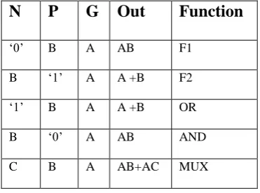
[image:1.595.336.522.626.764.2]GDI method is based on the use of a simple cell as shown in figure 2. At the first look the design is seems to be like an inverter, but the main differences are 1) GDI consist of three inputs- G (gate) input to NMOS/PMOS), P (input to source of PMOS) and N (input to source of NMOS). (2) Bulks of both NMOS and PMOS are connected to N or P (respectively), so it can be arbitrarily biased at contrast with CMOS inverter. Table 1 show, as discussed in, how a simple change of the input configuration of the simple GDI cell corresponds to very different Boolean functions. Most of these functions are complex (6- 12 transistors) in CMOS, as well as in standard PTL implementations, but very simple (only 2 transistors per function) in GDI design method
Table 1: Various logic functions of GDI cell for different input configurations
N
P
G Out
Function
‘0’ B A AB F1
B ‘1’ A A +B F2
‘1’ B A A +B OR
B ‘0’ A AB AND
1.2 Pass Transistor Logic
Another very popular design is Pass Transistor Logic design. When an NMOS or PMOS is used alone as an imperfect switch, we sometimes call it a Pass Transistor. PTL reduces the numbers of transistors used to make different logic gates, by eliminating excess amount of transistor. Transistors are used here as switches to pass logic levels between nodes of a circuit, instead of as switches connected directly to supply voltages (Vdd)
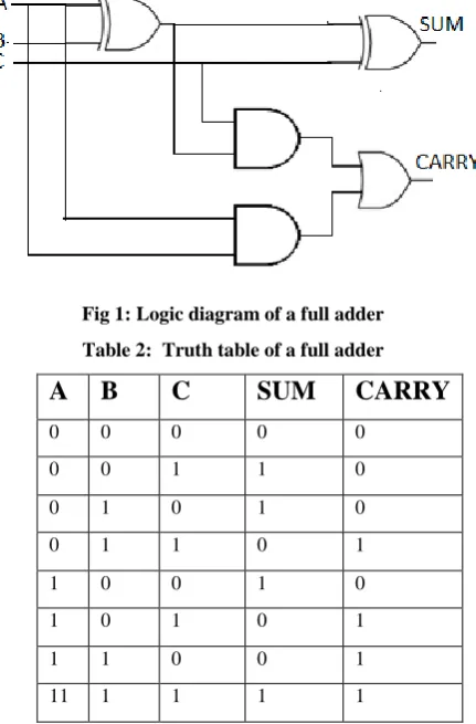
1.3 Full adder
A full adder could be a combinational circuit that forms the arithmetic sum of three input bits. It consists of three inputs and two outputs. In our design, we have designated the three inputs as A, B and C. The third input C represents carry input to the first stage. The outputs are SUM and CARRY. Fig 1 shows the logic level diagram of full adder. The Boolean expressions for the SUM and CARRY bits are as shown below.
B C
CARRY = A
.
B +A.
CIN + B.
C [image:2.595.61.277.415.743.2]SUM bit is the EX-OR function of all three inputs and CARRY bit is the AND function of the three inputs. The truth table 2 of a full adder is shown in Table 2. The truth table also indicates the status of the CARRY bit; that is to say, if that c array bit has been generated or deleted or propagated. Depending on the status Fig 1 Logic diagram of a full adder, depending on the status on input bits A and B, the CARRY bit is either generated or deleted.
Fig 1: Logic diagram of a full adder
Table 2: Truth table of a full adder
A
B
C
SUM
CARRY
0 0 0 0 0
0 0 1 1 0
0 1 0 1 0
0 1 1 0 1
1 0 0 1 0
1 0 1 0 1
1 1 0 0 1
11 1 1 1 1
If either one of A or B inputs is ‘1’, then the previous carry is just propagated, as the sum of A and B is ‘1’. If both A and B are ‘1’s then carry is generated because summing A and B would make output SUM ‘0’ and CARRY ‘1’. If both A and B are ‘0’s then summing A and B would give us ‘0’ and any previous carry is added to this SUM making CARRY bit ‘0’. This is in effect deleting the CARRY. To construct an n-bit
Here we proposes the Wallace tree multiplier using full adder the below block diagram shows the design of our multiplier where the AND gates produce the input to the system where they are finally produced [2] out from our adders where they do not require any carry-look ahead adder or ripple carry adder for final summing as so, there is a reduced usage of gates in the multiplier. The products of our multipliers are marked as P0, P1, P2, P3, P4, P5, P6, and P7 respectively. Hence our system not only replaces the half adders but also no separate final summing system is needed thus it occupies less area and works on low power.
The AND gate block diagram where the outputs produced by it are given to the full adder cells designed in Wallace tree structure the generated product terms are given as m0,m1,m2,m3,m4,m5,m6,m7,m8,m9,m10,m11,m12,m13 and m14 . The inputs which are fed to it are being processed and their outputs are generated respective to the multiplier design where the c inputs of some full adder predefined as 0 such that the full adders replace the half adder usage in the system. Various combinations of inputs are provided to gate structure to check and verify the full adders working performance.
1.4 Ripple carry adder
In RCA, the CARRY bit ripples all the way from first stage to nth stage. The delay in a RCA depends on the number of stages cascaded and also the input bits’ patterns. In the input patterns, a CARRY is neither generated nor propagated. On the other hand, certain input patterns generate carry bit in the first stage itself, which have to ripple through all the stages. This might increases the delay in the circuit. The propagation delay of such a case, also called critical path, is known as worst-case delay over all possible input patterns. In a ripple carry adder, the worst-case delay happens when a carry bit propagates all the way from least significant bit (LSB) position to most significant bit position (MSB).
The total delay of the adder will be an addition of delay of a SUM bit and delay of a CARRY bit multiplied by number of bits minus one in the input word.
T adder = (N-1) T carry + T sum
A0 B0 A1 B1 A2 B2 A3 B3
Cin C0 C1 C2 C3
[image:3.595.55.279.73.165.2]SUM0 SUM1 SUM2 SUM3
Fig 2: Block diagram of a 4-bit ripple carry adder
The logic function of XOR gate can be realized using MIFG CMOS transistors. The full adder constructed with MIFG devices uses only eight transistors, four MIFG transistors and four conventional transistors. The XOR logic in MIFG CMOS required for generating the SUM output of the full adder. The unit size capacitance is 500 F and other capacitors are integral multiples of the unit size capacitor.
A B
COUT
…
CINS
[image:3.595.54.276.270.356.2]
Fig 3: Example of a 16-bit ripple-carry adder
The implementation of a wide adder is the ripple-carry adder (RCA) where N full-adder cells are connected in series. This structure yields an area- and power- efficient adder with the demerits of a delay of the order of O (N). One way to speed up the RCA is to take advantage of the inverting property of full-adder cells:
(CS (A; B; COUT IN(A; B; C)=S(A; B;C)=COUTIN)
Then inverters can be avoided from the critical carry path. As described in the (A; B; C) previous this transformation also significantly reduces the power dissipation of the RCA.
1.3 Multiplier
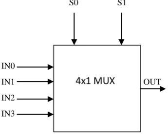
The output of the multiplexer stage is considered as input to the full adder. 4 to 1 MUX at the input and output stage selects the signals depending on the operation being performed [3].Transmission gates select one of the inputs based on the value of the control signal.
S0 S1
IN0
IN1 OUT
IN2
IN3
Fig 4: Block Diagram for mux
1.3.1 The New Multiplexer-Based Full Adder
In this part a 1-bit full adder that uses a multiplexer-based architecture, built upon 6 identical multiplexer gates. Substituting each of the multiplexer gates with a 2-transistor circuit gives us the new MBA-12T adder, which requires a total of 12 transistors to do the function of a full adder.
There will be three major sources of power dissipation in a digital CMOS circuit: logic transition, short-circuit current and leakage current .In the following, It is considered to show how low power consumption is achieved in the new MBA-12T adder due to reduction in short circuit current and switching activity. The short-circuit current is considered to be the direct current passing through the supply and the ground, If both the NOMS and PMOS transistors are simultaneously active. The SERF, 10T-09A, 10T09B, and 10T13A adders all suffer from the same short-circuit current problem as they have some internal nodes driven by signals with slow raise and/or fall times. This leads to significant (20%) short circuit power dissipation for loaded inverters .Such problem was partially solved in SERF, 10T09A, and 10T09B adders.
2. MICROWIND
2.1 General Introduction
This is truly integrated EDA software compassing IC designs from concept to completion, enabling chip designers to design beyond their imagination. It integrates traditionally separated front-end and back-end chip design into an integrated flow, accelerating the design cycle and reduced design complexities in working in Micro-wind tool. It tightly integrates mixed-signal implementation with digital implementation, circuit simulation, transistor-level extraction and verification in providing an innovative education initiative to help individuals to develop the skills needed for design positions in virtually every domain of IC industry.
It also supports entire front-end to back-end design flow. The front-end designing is done by using DSCH (digital schematic editor) which consists of built in pattern based simulator for digital circuits. The user can also build analog circuits and convert them into SPICE files and use 3rd party simulators like Win Spice or PSPI CE. DSCH3.5 can convert the digital circuits into Verilog file which can be further synthesized for FPGA/CPLD devices of any vendor. The same Verilog file can be compiled for layout conversion in MICROWIND [4].
The back-end design of circuits is done by MICROWIND. User can also design digital circuits and compile here using Verilog file. MICROWIND automatically generates an error free CMOS layout. The route is not optimized enough as that which does not indulge in complex place & route algorithms. User can also create CMOS layout of their own using compile one line Verilog syntax or custom build the layouts by manual drawing. The CMOS layouts can be verified using inbuilt mix-signal simulator and analyzed further for DRC, cross talks, delays, 2D cross section, 3D view.
2.2 Power Delay Product
In digital electronics, the power–delay product is a figure of merit correlated with the energy efficiency of a logic gate or logic family. This is also known as switching energy, it is the product of power consumption (averaged over a switching event) times the input–output delay, or duration of the switching event. It has the dimension of energy, and measures the energy consumed per switching event.
FULL ADDER
FULL ADDER
FULL ADDER
FULL ADDER
FA
0
0
FA
FA
FA
15
[image:3.595.55.228.592.730.2]2.2.1 Power Dissipation in CMOS
The component of power to be considered during the input signal transition, and consists of two parts, a dynamic dissipation and short circuit. The dynamic power is dissipated to modify the charge content of the capacitive load, it is proportional to the switching frequency and to the load capacitance, and hence depends on the area of the buffers. The short circuit power dissipation is produced by the simultaneous conduction of P and N transistors during the transition of the input signal. The ratio of input to transition times is a good indicator of short circuit power dissipation. The ratio values comparable or lower than unity, which is the objective of buffer design, the short circuit power dissipation can be omitted. Buffer design with fixed or variable tapering factors has been obtained with short circuit power content lower than 10% of the total power dissipation. The result, in the definition of our optimizing objectives, is to just consider the dynamic component. CREF tot is the total value of the load capacitances involved in the design, it includes layout parasitic (diffusion and interconnect) and active loads is the minimum capacitance considered in the design methodology or in the library.
2.2.2 Design for minimum Power delay product
In this part an explicit expression for the power- delay product of inverters and compare design solutions, for the minimum of this product, to the alternatives investigated in the preceding parts. The delays in CMOS structures depend on the ratio of the total load to the drive capacitance of each cell, and that this ratio could be expressed (θ) as a fractional part of a reference capacitance, (C REF ) used as a measure unit for the
load. The total dynamic power as the product of a reference power, , by the total load capacitance normalized with respect to the reference capacitance For an array of 2 inverters this results in.[5].The power-delay product can then be obtained as where CIN1=(1+k)CN) defines the reference capacitance. Derivative of this expression with respect to CIN2gives the optimum tapering factor minimizing the power-delay product.
2.2.3 Delay area and Power consumption
Comparison between n-bit classic three-operand and proposed n-bit Three-operand multiplier can be designed by subtracting the delays computed by each of the designs. The corresponding delay for three-operand multipliers using classic method of multiplication is the problem in now ever days architectures. Subtracting computed delay of each design from equation would tell us which approach is faster. In case of proposed design I, as it was mentioned the delays are equal but because of cellular architecture used in proposed design I, It is considered that it is faster than classic method of multiplication. Subtracting equation from will tell us which approach is faster, comparing classic three operand multiplications and proposed design II.
As it is evident from the derived equation, the proposed design II is faster by number computed by equation with respect to classical method of multiplication. Performing the same procedure as proposed design II for proposed design III and subtracting will give us the difference [6]. For performance evaluation and comparison, we use logical effort and will show the delay of each proposed design. In this case, delay of an AND gate is delay of one gate shown by d(AND), the delay of a 4:2 compressor is equal to 3 gates denoted by d(4:2), and latency of a XOR is 2 gate delay, indicated by d(XOR). In order to ease the comparison produced to show the practical delay based on logical effort analysis.
2.3 High Speed Addition
First thing is to examine a realization of a one-bit adder which represents a basic building block for all the more elaborate addition schemes.
2.3.1 Full Adder
Operation of a Full Adder is defined by the Boolean equations for the sum and carries signals: Where ai, bi, and ci are the inputs to the i-th full adder stage, and si and c are the sum and carry outputs from the i-th stage, respectively. The realization of the Sum function requires two XOR logic gates. The Carry function is further rewritten defining the Carry-Propagate pi terms and Carry-Generate gi terms: At a given stage i, a carry is generated if gi is true (i.e., both ai and bi are ONEs), and if p is true, a stage propagates an input carry to its output (i.e., either ai or b is a ONE). Fig.1. Full-Adder implementation (a) regular (b) using multiplexer in the critical path For this implementation, the delay from either a or bi to si is two XOR delays and the delay from ci to ci+1i is 2 gate delays. Some technologies, such as CMOS, implement the functions more efficiently by using pass-transistor circuits. For example, the critical path of the carry-in to carryout uses a fast pass-transistor multiplexer [8] in an alternative implementation of the Full Adder
3. SIMULATION ENVIRONMENT
3.1 Various Circuits
The performance of 7 full-adders, named: new14T , hpsc , hybrid , hybrid cmos , cpl . The schematics and layouts were designed using a TSMC 0.18m CMOS technology, and simulated using the BSIM3v3 model and the post-layout extracted netlists containing parasitic. Simulations were carried out using Nanosim to determine the power consumption features of the designed full-adders, and Hspice to measure the propagation delay for the output signals. In order to have a good comparison, It is must to take the transistors sizes for each full-adder.
The simulation results for full-adders performance comparison, regarding power consumption, propagation delay, and PDP. All the full-adders were supplied with 1.8 V and the maximum frequency for the inputs was 200 MHz. It is worth to observe that in some cases, the power consumed from the power-supply (power supply) for the full-adder is smaller than the total average power (avg power). This is because of, for some logic styles (e.g., pass-transistor style); some current is taken from the inputs of the full-adder and is used to charge the internal nodes. As mentioned above, it is the importance of considering the power consumption of the input buffers in the top test-bed.
From the results in Table 3,
•The implementation area obtained from the layouts, it can be seen that the proposed full-adders require the smallest area (up to 40% of relative area), which can also be considered as one of the factors for presenting lower delay and power consumption, as it implies smaller parasitic capacitances being driven inside the full-adder.
The reason for the smaller area, compared to other full-adders that have less transistors, is that the size of the transistors in the proposed full-adders is minimal and not larger than 2m (except for the symmetrical response inverters at the inputs), while for other full-adders the transistor[9] sizes are the range of 4 to 6m. the layouts of the proposed full-adders, with the correspondent side by side dimensions.
• Finally, it is determined that the maximum frequency that each full adder can operate, while being supplied with 1.8 V. The proposed full-adders reach up to 1.25 GHz, only surpassed by cpl cell, at the expense of major power consumption and area. The reason for running the power-delay performance simulations at 200 MHz was due to the full adders that work only up to 250 MHz.
3.1.1 DPL Circuit
[image:5.595.316.536.71.232.2]The schematic circuit for DPL is shown below
Fig 5: DPL circuit diagram
3.1.2 DPL Layout
[image:5.595.349.521.319.525.2]The simulation layout for DPL is generated using the Microwind tool.
Fig:6: DPL Layout
3.1.3 DPL Graph
The waveform generation of DPL circuit is shown below
Fig 7: DPL Graph
The above waveform is generated by giving the inputs to A is ‘0’, B is’0’and Cin is ‘0’.The output in SUM is low and the carry is also low. Similarly A is ‘1’, B is ‘1’and Cin
is’1’.The output of SUM is’ high’ And the carry is also ‘high’. Likewise the next combination of the inputs A, B, C we get output waveform with respect to it.
Fig 8: Full-adder designed with the proposed logic structure and a SR-CPL logic style
Based on the results obtained in, two new full-adders have been designed using the logic styles DPL and SR-CPL, and the new logic structure presented in figure. It is designed using a DPL logic style to build the XOR/XNOR gates, and a pass-transistor based multiplexer to obtain the so output. In Fig. 10 the SR-CPL logic style was used to build these XOR/XNOR gates. In both cases, the AND/OR gates have been built using a powerless and groundless pass-transistor configuration respectively, and a pass-transistor based multiplexer to get the Co output.
3.1.4 SRCPL Circuit
[image:5.595.59.274.348.482.2] [image:5.595.56.273.551.691.2]Fig 9: SR-CPL Layout
3.1. 5 SR-CPL Layout
[image:6.595.319.534.77.218.2]The layout for SR-CPL is shown below
Fig 10: SR-CPL Layout
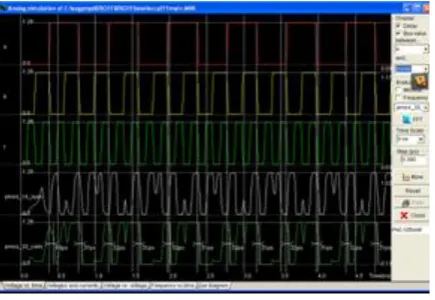
3.1.6. SR-CPL Graph
[image:6.595.54.274.256.421.2]The above waveform is generated by giving the inputs to A is ‘0’ ,B is’0’and CIN is ‘0’.The output in SUM is low and the carry is also low. Similarly A is ‘1’, B is ‘1’and CIN is’1’.The output of SUM is’ high’ And the carry is also ‘high’. Likewise the next combination of the inputs A, B,C we get output waveform with respect to it[10]
Fig 11: SR-CPL Graph
Table 3: Power In µW, Delay In p s , Area In µ W
4. CONCLUSION
The alternative internal logic structure for designing full-adder cells was been introduced. Hybrid design style gives more freedom to the designer to select different modules in a circuit depending upon the application. Using the adder categorization and hybrid design style, many full adders can be conceived. Here two novel full adders are designed using GDI design as well as PTL-GDI design style are presented in this paper that targets low PDP. The proposed hybrid full adders have better performance than most of the standard full-adder cells owing to the novels design modules proposed in this paper. It performs well with supply voltage scaling. From the comparison table 3 it can be inferred that both the proposed designs are good performer at different supply voltage conditions. However both the designs have their own advantages. They are the supply voltage is above the threshold voltage (for example 3V, it is suggested to use Proposed PTL-GDI Adder. If the adder is to be used in a wide range of supply voltages (for example 0.8V-3V), it is suggested to use the Proposed GDI design. Considering Delay into account both the designs are found to be best in different supply voltages. In order to demonstrate its advantages, two full-adders were built in combination with pass-transistor powerless/groundless logic styles. They were designed with a TSMC 0.18m CMOS technology, and were simulated and compared against other energy-efficient full-adders reported recently. Hspice and Nanosim simulations showed power savings up to 80%, and speed improvements up to 25%, for a joint optimization of 85% for the PDP. The area utilization for the proposed full-adders is only 40% of the largest full-adder compared, and the power-supply voltage for the proposed full-adders can be lowered down to 0.6 V, maintaining proper functionality.
5. REFERENCES
[1] S. Agarwal., V. K. Pavankumar., and R. Yokesh., “Energy-efficient high performance circuits for arithmetic units,” in Proceeding of 2nd International Conference on VLSI Design, January. 2008, pp. 371– 376.
[2] M. Aguirre., and M. Linares., “An alternative logic approach to implement high-speed low-power full adder cells,” in Proceeding of SBCCI, Florianopolis, Brazil, September. 2005, pp. 166–171.
[3] K. M. Chu.,and D. Pulfrey., “A comparison of CMOS circuit techniques: Differential cascode voltage switch logic versus conventional logic,” IEEE Journal of Solid-State Circuits, vol. SC-22, no. 4, pp. 528–532, August . 1987.
[image:6.595.56.274.519.669.2]circuits,” IEEE Transaction of Very Large Scale Integration (VLSI) Systems , vol. 13, no. 6, pp. 686– 695, January. 2005.
[5] S. Goel., A. Kumar., and M. Bayoumi., “Design of robust, energy-efficient full adders for deep-submicrometer design using hybrid-CMOS logic style,” IEEE Transaction of Very Large Scale Integration. (VLSI) Systems, vol. 14, no. 12, pp. 1309–1320, December. 2006.
[6] D. Patel., P. G. Parate., P. S. Patil., and S. Subbaraman., “ASIC implementation of 1-bit full adder,” in Proceedings of 1st International Conference on Emerging Trends Engineering Technology , July . 2008, pp. 463–467.
[7] D. Radhakrishnan., “Low-voltage low-power CMOS full adder,” IEEE Proceedings of Circuits Devices Systems , vol. 148, no. 1, pp. 19–24, February . 2001.
[8] A. M. Shams., and M. Bayoumi., “Performance evaluation of 1-bit CMOS adder cells,” in Proceedings of . IEEE ISCAS, Orlando, FL, May 1999, vol. 1, pp. 27– 30.
[9] M. Suzuki., M. Suzuki., N. Ohkubo., T. Shinbo., T. Yamanaka., A. Shimizu., K. Sasaki., and Y. Nakagome., , “A 1.5 ns 32-b CMOS ALU in double pass-transistor logic,” IEEE Journal of Solid-State Circuits, vol. 28, no. 11, pp. 1145–1150, November . 1993.
[10] M. Zhang., J. Gu., and C. H. Chang., “A novel hybrid pass logic with static CMOS output drive full-adder cell,” in Proceedings of IEEE International Symposium of Circuits Systems, May 2003, pp. 317–320.