Invited Paper
Realization of Three-Dimensional Micro
and Nano-Structures on Silicon Substrates
S. Azimi
1, S. Mohajerzadeh
1;, A. Amini
1, A. Vali
1and M. Mehran
1 Abstract. The realization of nano and micro-sized, highly-featured, 3-dimensional structures on Si substrates is reported where a single mask in a hydrogen-assisted deep reactive ion etching is exploited. Three main gases of oxygen, hydrogen and SF6 are used in a sequential passivation and etching processto achieve high aspect ratio features. The ows of gases, and the plasma power and timing of each subsequence are the main parameters to achieve the desired three-dimensional etching by controlling the under-etching and recovery steps, which leads to the formation of unique features directly on silicon substrates. Depending on the plasma power, etch-rates as high as 0.75 m/min can be obtained. The plasma power can reach a high value of 1 W/cm2 over a large area of 20 15 cm2. In addition, features
with a controllable under-etching and a recovery with more than 8 m in the sidewall recession have been achieved. Furthermore, values of aspect ratios higher than 40-50 can be obtained. The formation of nano-wall features is also reported.
Keywords: Vertical etching; Deep reactive ion etching; 3-D structures; Curved nano-walls.
INTRODUCTION
Deep vertical etching and especially three-dimensional (3-D) structures are promising features for optical and mechanical applications. Conventionally, 3-D struc-tures refer to those where height, as the third dimension of the feature, is controlled during the vertical etching process. These structures can be regularly realized using multiple lithographies. Recently, however, a single masking layer fabrication process has been intro-duced using deep reactive ion etching combined with gray scale lithography [1-4]. The evolution of Micro-Stereo-Lithography (MSL) has been shown to be a powerful technique to achieve high-aspect-ratio, three dimensional structures on polymers, where the height remains constant but where the structure possesses complex features in the z-direction. In this technique, a UV laser illumination is used to create sections on a UV-curable polymer to form the desired shape [5].
MSL enjoys high accuracy and miniaturization power but it is not immediately applicable to silicon 1. Electronic Center of Excellence, Thin Film and Nano-Electronic Lab, School of Electrical and Computer Engineer-ing, University of Tehran, Tehran, P.O. Box 14395/515, Iran.
*. Corresponding author. E-mail: [email protected] Received 27 May 2010; accepted 25 September 2010
substrates and requires a polymeric coating. Due to its natural polymerization and exposure, it is considered as a serial fabrication process, making it time con-suming and expensive. Nevertheless, it can be used as a method to form three-dimensional features on silicon substrates after a micro-molding step is carried out [6]. Apart from micro-scale features, sub-micro and nanostructures with three-dimensional features are realized using a glancing low angle deposition and layer engineering technique [7,8]. Such three-dimensional features are suitable candidates for optical applications, where wavy metallic nanowires are formed on glass and silicon substrates during lm deposition.
The advent of silicon micromachining has been an important step towards the realization of various 3-D features [9]. Complex devices, such as pressure sensors, accelerometers, gyroscopes, optical mirrors and switches, RF devices, lters and micro-motors, lend their success to the advent of silicon microma-chining and its outcomes, where the anisotropic eects of etching chemistry are combined with the isotropic plasma-based chemistry to achieve desired shapes and features [10-16]. Apart from wet chemical etching pro-cesses, the use of a dry etching tool, especially plasma-based reactive ion etching, is a complementary tech-nique to achieve high aspect ratio 3-D structures [9].
(DRIE) has been a great milestone in modern micro/nano-electromechanical systems. A process which was rst reported by the Bosch Company in 1998 utilizes a sequential etching and passivation steps to form vertical trenches and walls onto silicon sub-strates with high-aspect ratio and controllable sizes and depths [17]. The consecutive use of a polymeric coating during the passivation cycle guarantees the protection of the sidewalls of the etched craters, while the bottom of the etched region is removed with the aid of high density Inductively Coupled Plasma (ICP). The etching subsequence is also achieved using RF-plasma with a reactive gas like SF6. The formation
of vertical features with aspect-ratios as high as 100:1 has been reported [18]. A non-sequential cryogenic process has also been introduced, taking advantage of a mixture of oxygen and SF6 for the etching of
silicon substrate with no need for a polymeric coating step. The key parameter in this technique is to maintain the substrate at a cryogenic temperature (-110C) during the etching [19]. The concurrent use of
SF6 and oxygen during the etching, with the addition
of chlorine-based gases, allows the formation of high-aspect ratio features at ambient temperatures. The use of inductively-coupled plasma is a critical component in all the reported etching techniques [20].
Recently, we have developed a deep reactive ion etching process, which neither needs high-density plasma nor uses external polymeric coating or cryo-genic temperature arrangements. In our novel tech-nique, the vertical etching of silicon substrate is achieved using a sequential etching and passivation sub-cycles, as reported elsewhere [21]. Our process exploits a combination of three main gases of hydrogen, oxygen and SF6 in a reactive ion etching unit with a
RF plasma source, although nitrogen or argon can also be incorporated to purge the chamber between gas-switching. The etching is divided into two or three sub-cycles (etching/passivation) where a mixture of H2/O2/SF6constituents is used during the passivation
cycle, while the next subsequence (etching) is achieved merely with SF6 as the feed gas. In this paper, for the
rst time, the creation of ultra-small, highly featured, three-dimensional structures with curved sidewalls is reported.
Unique nano-metric features suitable for elec-tronic and photonic devices, are reported. The etch-ing and passivation sub-sequences are programmed in order to achieve the under-etching and recovery steps which form the desired three dimensional fea-tures. A potential application of these 3-D silicon structures is in soft lithography, where they can be used as micro/nano-molds, suitable for tissue and biocompatible engineering [22,23]. Next, we describe our deep reactive etching technique followed by the experimental procedure for the formation of
three-dimensional structures. Images have been obtained using a SEM unit operating at 15-30kV and with a secondary electron detector.
EXPERIMENTAL SETUP
P-type 1-5 cm single side polished silicon wafers are used for this investigation. The etching and fabrication processes are based on our recently reported deep reactive etching technique, where a sequential etching/passivation procedure is employed [21]. The etching is achieved in a Reactive Ion Etching (RIE) machine operating at 13.56 MHz plasma with an eective area of 20 15 cm2. A RCA # 1 solution
(NH4OH:H2O2:H2O, 1:1:5) is used to clean the samples
prior to any lithographic step. The cleaning step is critical to avoid grass or black silicon formation. The cleaned samples are placed in an electron-beam evaporation system to deposit a 0.1 m-thick layer of Cr. The base pressure for this deposition step is 1 10 6 torr. The Cr-coated samples are patterned using
standard high precision photolithography (projection lithography) to act as a mask for the subsequent etching process and to realize the desired micro and nano-structures.
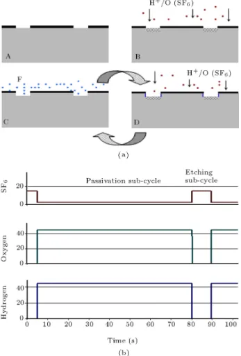
Figure 1 shows the schematic of the etching process, illustrating both the passivation and etching sub-cycles. For a three-dimensional etching, the un-deretching is controlled by adjusting the power, gas mixture and duration of the passivation sub-cycle. The evacuation of the reactor is systematically practiced by means of a mechanical pump and the mixture of hy-drogen and oxygen gases is fed into the reactor. These two steps are repeated as many times as required to achieve the desired depth. We believe that during the passivation step, the existence of the hydrogen atoms not only assists in the formation of a thin protective layer on the side-walls of the etched pit, but also bombards the bottom of the crater to impart defects to the exposed silicon surface, hence improving silicon removal in the subsequent etching step. The total etch rate depends on the etching depth during the etching subcycle, as well as on the total duration of a complete cycle. By controlling the etching parameters, one is able to achieve etch-rates as high as 0.75 m/min, while achieving an aspect ratio of 10 and more. If the etch-rate is lowered to values less than 0.4 m/min, a high aspect ratio up to 40-50 can be obtained.
Since this technique does not use Inductive-Couple-Plasma (ICP), an accurate control over im-portant parameters of the process, i.e. gas-ows, plasma power and cycle-duration, are crucial to achieve complex and high-aspect ratio features. Figure 1b represents a schematic gas-ow versus time for the whole etching/passivation cycle. This cycle is repeated as many times as required to achieve the desired
Figure 1. (a) Process steps of deep silicon vertical etching (from A to D). The etching requires a passivation subcycle plus an etching sub-cycle to achieve a deep vertical etching. (b) A schematic gas ow for three gases used in this technique. Typical gas ow rates are 45:45:3 sccm for H2:O2:SF6 gases during the passivation
subcycle, respectively. During the etching subcycle, only SF6 ows into the chamber with a ow of 15 sccm.
shape and depth of the crater. As seen from this gure, during the passivation step, all three gases are introduced into the reactor. Typical values for the O2/H2 mixture as the main constituent in this
period are 45-50 sccm, whereas SF6 ows with a
low value of 3 sccm. The plasma power is another important parameter in this subcycle and it has a typical value ranging from 150 to 250 W during this subcycle. The duration of this subcycle can be widely varied, ranging from a short treatment of 30 seconds in high speed etching to 120 seconds for high resolution and high aspect ratio etching processes. The etching subcycle is achieved by switching o the H2/O2 gases
and increasing the value of the SF6 ow rate to
15-20 sccm. The duration of this subcycle is less and ranges between 10 and 20 seconds, with a typical value of 15 seconds and a typical plasma power of 140 W. Usually, two intermediate purging steps are needed to
ensure that proper switching between gases is achieved. These steps might be as short as 5 seconds, although typical values are 15 seconds for each. So the total duration of an etching cycle can range from 55 to 160 seconds. The overall etch rate can be between 0.25 to 0.75 m/min, although higher etch-rates up to 1 m/min are expected.
RESULTS AND DISCUSSIONS Vertical Etching
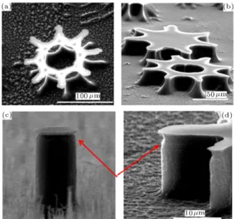
Figure 2 collects several SEM images for the etching process prepared for this study. The top-right image in this gure corresponds to a high aspect ratio etched thin rod. The thickness of the rod is 150 nm and the
Figure 2. The collection of several SEM images of samples processed by silicon vertical etching with various heights and sizes. The smiley face structure has 8 m height and aspect ratio of 30:1. Deep etching down to 100 m is also observed in this gure. Arrows in the middle images show the height (25 um) and width (500 nm) of rods. These images represent a highly ordered array of deep sub-micrometer rods and needles with sizes below 300 nm and heights over 20 m. The bottom-left image belongs to vertical nano-metric features with dierent sizes down to 140 nm and an aspect ratio of the order of 50.
height of the structure is around 6 m. In addition, other small features, like a smiley face, have been vertically etched with a high aspect ratio of more than 30:1. The evolution of vertical holes with a height of 100 m is observed in the bottom-right image. The opening of the hole is about 120 m and the under-etching is less than 5 m. The bottom images in this gure belong to arrays of silicon nano-rods where highly ordered features with a height of more than 20 m and width less than 300 nm are observed. Figure 3 depicts the result of the vertical etching of silicon using this technique to study the size-dependent etch rate or the so-called RIE lag. As seen from this image, the etch depth for an opening of 1-2 m is slightly less than the etch depth for a higher opening of 20 m. For this experiment, the etch depth is around 20 m and a modest drop is observed for smaller openings. Figure 4 shows the SEM images of ultra small features down to 100 nm.
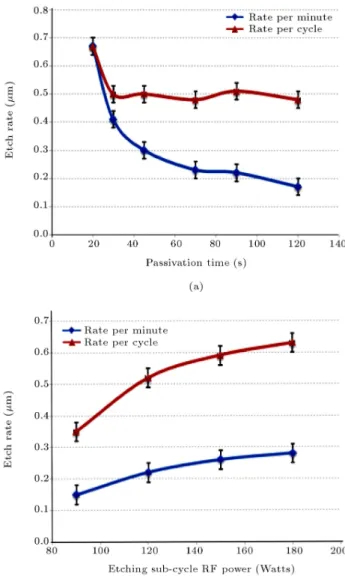
In order to observe the eect of the passivation time on the total etch rate, we have selected the etch
Figure 3. The observation of RIE lag for small openings (top) and channels (bottom). For a small opening of 1-2 m, there is a slight drop in the etch rate. The red line in both gures compares the bottom of a large opening with smaller features. As seen, the depth of the narrower opening is slightly less than the larger windows, which is called \RIE-lag".
Figure 4. (a) Etch rate versus passivation time where the duration of the etch sub-cycle has been xed at 15 seconds. If the passivation time exceeds 2 minutes, etch rate drops considerably to less than 0.2 m/min. (b) Etch rate versus RF power during the etching sub-sequence. As seen by raising the plasma power, the total and sequence etch rates greatly increase.
parameters as given in Table 1. The etching sub-cycle has a determining eect on the total etch rate and mask under-cut. An important parameter in obtaining three-dimensional structures is the passivation time whose eect on the etch rate is given in Figure 4. As seen from this gure, by going to higher passivation times, the rate per sequence drops due to further passivation of the crater bottom. However, the total etch rate shows a more magnied drop mainly due to the addition of extended time to the total etching period. A maximum etch rate of 0.65 m/min is observed from this curve obtained for a passivation sub-cycle of 15 seconds. The etching sub-cycle has been set at 15 seconds. with a plasma power of 150 W over an area of 15 20 cm2.
Table 1. Etching parameters selected to investigate the eect of sweeping the passivation time. Sub-Cycle Duration
(Sec)
RF Power (Watts)
SF6 Flow
(sccm)
O2 Flow
(sccm)
H2 Flow
(sccm)
Chamber Pressure (mTorr)
Passivation 20-120 200 3 45 45 380
Etching 10-15 150 16 0 0 120
obtained by increasing the duration of the etching of the sub-cycle. For instance, by raising this time to 20 seconds and keeping the passivation time at 30 seconds, it has been possible to obtain a total rate of 0.75 m/min.
Three-Dimensional Etching
Figure 5a depicts the SEM image of a sample with a severe under-etch, which leads to complete damage of the original mask and the obtaining of an undesired crown-like structure out of the gear mask. To obtain such a sample, the hydrogen gas has been switched o during the passivation sub-cycle and no sign of vertical etching is observed. In Figure 5b, the same structure has been examined with a lower amount of underetch, suitable for three-dimensional fabrication. For this sample, the hydrogen gas ow has been set at 15 sccm, as opposed to 45 sccm for a normal vertical etching
Figure 5. (a) Severe under-etch results in a crown-like structure. The gear-like chromium mask is remained on top of the structure. (b) The same structure with a lower amount of under-etch suitable for three-dimensional fabrication. The control over underetching is an important factor for the formation of highly featured
three-dimensional structures. (c) and (d) Similar structures etched with some under-etching at the rst steps, followed by high aspect ratio vertical etching. Arrows show where the under-etch has recovered.
process. Controlling the underetching is an important factor in the formation of highly featured, three-dimensional structures. By properly adjusting the H2/O2 plasma conditions during the passivation
sub-cycle, the desired 3-D shapes are realized. Interestingly, it is possible to realize a reverse underetching, which we refer to as recovery, by similar controlling tools. In Figure 5d, a combination of underetching with vertical removal is depicted. The arrow in this gure points out the recessed region due to a desired underetching step. Once the gas ows have been set back to their optimum values for vertical etching, sharp walls are obtained.
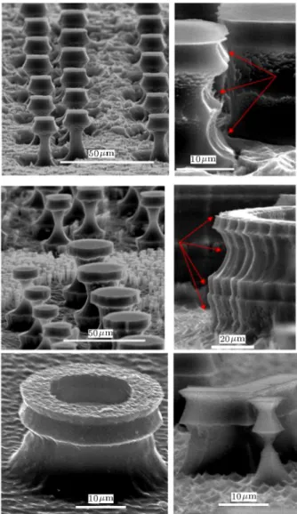
Figure 6 collects many samples prepared, using this underetching/recovery technique. Figure 6a shows an unusual reversed glass-like structure where the initial intentional underetching has been fully recovered
Figure 6. Some silicon 3-D structures obtained from controlled under-etch during the vertical (anisotropic) etching process. (a) An unusual sample, where the initial underetching has been recovered and the remainder of the process has been vertical. Elimination of hydrogen during the passivation process for the rst ve etching sequences has led to the severe underetching, whereas for the remaining 45 sequences, the recipe is the same as that used for the results in Figure 2. (b) The same shapes, but in this case, the rst 5 steps of etching are vertical and, thus the underetching is observed at a lower height. (c) and (d) are opposite in the sense that initial etching sequences (40) are vertical and the last 10 sequences are without a hydrogen ow to create underetching.
and a vertical etching has been evolved. For this sam-ple, the initial etching has been carried out by turning \o" the hydrogen gas to minimize the passivation of the side-walls. As observed, the sample has undergone a severe underetching over this period, which took \ten" etching cycles. After this underetching period, the hydrogen gas has been turned \on" and the normal etching process has been set. Under such conditions, the further progress of underetching has stopped and a recovery is observed. After 25 cycles of normal etching, the original round mask has been recovered and the further progress of the etching results in an almost vertical structure. The presence of grass-like features or black-silicon at the very bottom of the sample surface is observed in this gure, which could be diminished by a quick exposure to SF6 plasma with a low power
of 100 W. Other images of this gure belong to cases where a vertical etching process has been practiced, initially followed by a low hydrogen gas ow to ensure moderate underetching over the subsequent cycles. It is worth mentioning that similar shapes can be obtained using a micro-stereo-lithography technique. However, a polymeric substance is used for such a 3-D conguration instead of silicon substrates.
In Figure 7 we have shown schematically how complex 3-D structures are realized and repeated. Steps \A" to \F" are needed to form a curved structure. It must be borne in mind that the depth of the curved sidewalls can be as much as 20 m, where many etching/passivation cycles are involved. After obtain-ing the rst curved feature, the sample is thermally oxidized in a dry-oxide furnace and the bottom SiO2
is removed using direct-current plasma hydrogenation carried out in a dc-plasma reactor. This step is crucial
Figure 7. The process steps of a desired 3-D shape silicon etching, starting with mask patterning (A), followed by etching with desired under-etching (B) and recovery (C), oxide passivation (D) and removal from the bottom (E). The nal structure depends on the number of times these steps are repeated (F).
to remove the oxide layer from the very bottom of the craters and can be obtained by a dc power of 1 W/cm2 in hydrogen plasma at a pressure of 1-5
torr. Once this oxide layer is partially removed, a quick dip in buered HF (hydrouoric acid) ensures the complete removal of the bottom oxide. Care should be taken not to aect the side-oxide to make sure that the subsequent etching will not aect the remaining features of the previous under-etching/recovery stages. At the present time, we are trying to avoid such an external oxidizing step by better optimization of the etching process.
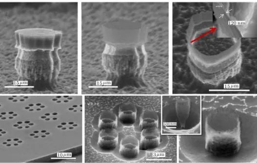
Figure 8 collects a set of SEM images for sev-eral samples, which have been prepared with three
Figure 8. SEM images of desired 3-D shape silicon etching. The under-etching has been as much as 8 nm m. By controlling the main gases, it has been possible to recover the recessed side-walls and obtain the original mask. The results presented in this gure correspond to one initial step of vertical etching (top), followed by one or two steps of under-etching/recovery. The curved and highly featured edges are evident from this gure.
Figure 9. The evolution of highly featured, three-dimensional nano-wall structures. The top images belong to the formation of nano-metric featured Si/SiO2 with a wall thickness below 120 nm. The bottom images show the formation of
ultra thin curved cup-like structures. The inset in the bottom line of the images depicts an ultra ne 3-D glass like SiO2
nanostructure, where features around 100 nm are observed.
sequences to form highly featured structures. As seen from these images, the overall underetching has been as much as 7 m in some of the samples. By controlling the main gases, it has been possible to recover the recessed sidewalls and obtain the size of the original mask. The results presented in this gure correspond to one initial step of vertical etching (top) followed by one or two steps of underetching/recovery. The curved and highly featured edges are evident from this gure. In addition, Figure 9 shows a collection of several SEM images of the samples, where 3-D nano-walls are easily observed. In this image, the thickness of the SiO2walls
has been measured to read a value of 120 nm. Such 3D structures can be used for polymeric molding, photonic crystal fabrication and mechanical resonators, in which the complex geometry of the vertical rods would aect their resonance behavior. Molded polymeric 3D micro-structures obtained from this technique can be used as scaolds for tissue engineering [22-23]. Further investigation into this technique to obtain nanometric features, to integrate the passivation in the same re-active ion etching machine, and to fabricate polymeric 3D structures is being pursued.
SUMMARY AND CONCLUSION
We have successfully demonstrated three-dimensional nano and micro-structures on silicon substrates using a novel deep reactive ion etching technique. This technique allows the high aspect ratio vertical etching of silicon substrate with no need for a polymeric coating or high-density plasma. Instead of a polymeric coating
for the passivation subcycle, a mixture of hydrogen, oxygen and SF6 gases is used, which not only protects
the sidewall, but also improves the verticality by bom-barding the exposed surface of the silicon substrate. The use of these gases allows a unique feature which allows the recovery of the underetched sidewalls. By controlling the gas ows during the passivation subcy-cle, it is possible to achieve the desired underetching, which can be recovered by proper setting of the gases in subsequent etching steps.
The formation of highly featured three-dimensional structures with SiO2 nanowalls has
also been demonstrated. These structures can be used in designing the photonic crystal arrays of vertical-standing rods, where apart from the desired order in the X Y plane, the order in the Z-direction adds up to the ltration capabilities of the array. The formation of ultra small features sheds light on the formation of more complex nano-structures suitable for single-electron and nano-electromechanical (NEMS) applications. By combining the polymeric molding and 3-D features of the fabricated structures, useful structures for tissue engineering can be realized. The fabrication of more complex structures and smaller features is being pursued.
ACKNOWLEDGMENT
This work has been supported by a grant from the Research Council of the University of Tehran. The au-thors are thankful to Professor Soleimani and Professor Fathipour for their support.
REFERENCES
1. Waits, C.M., Modafe, A. and Ghodssi, R. \Investiga-tion of gray-scale technology for large area 3D silicon MEMS structures", J. Micromech. Microeng., 13, pp. 170-177 (2003).
2. Rao, M.P., Aimi, M.F. and McDonald, N.C. \Single-mask three-dimensional microfabrication of high as-pect ratio structures in bulk silicon using reactive ion etching lag and sacricial oxidation", Applied Physics Letters, 85(25), pp. 6281-6283 (2005).
3. Martya, F., Rousseaua, L., Saadanya, B., Merciera, B., Francaisa, O., Mitab, Y. and Bourouina, T. \Advanced etching of silicon based on deep reactive ion etching for silicon high aspect ratio microstructures and three-dimensional micro- and nanostructures", Microelec-toinc Journal, 36, pp. 673-7 (2005).
4. Gantz, K., Renaghan, L. and Agah, M. \Develop-ment of a comprehensive model for RIE-lag-based three-dimensional microchannel fabrication", Journal of Micromechanics and Microengineering, 18, 025003 (2008).
5. Bertsch, A., Jiguet, S., Bernhard, P. and Renaud, P. \Microstereolithography: a Review", Mat. Res. Soc. Symp., 758, pp. 1411-1416 (2003).
6. Kanamori, Y., Sato, J., Shimano, T., Nakamura, S. and Hane, K. \Polymer microstructure generated by laser stereo-lithography and its transfer to silicon substrate using reactive ion etching", Microsystem Technologies, 13(8-10), pp. 1411-1416 (May 2007). 7. Rabbie, K. and Lakhtakia, A. \Chiral sculpture thin
lms" Nature, 384, p. 616 (Dec. 1996).
8. Horn, M.W., Pickett, M.D., Messier, R. and Lakhtakia, A. \Blending of nanoscale and microscale in uniform, large area, sculptured, thin lm architec-tures", Nanotechnology, 15, pp. 303-310 (2004). 9. Kovacs, G.T.A., Maluf, N.I. and Petersen, K.E. \Bulk
micromachining of silicon", Proc. IEEE, 86(8), pp. 1536-1551 (Aug. 1998).
10. Darbari, S., Azimi, S., Mohajerzadeh, S., Sammak, A., Izadi, N. and Famini, S. \Hydrogenation-assisted lateral micromachining of (111) silicon wafers", J. Microelectromech. Syst., 17(6), pp. 1489-1494 (Dec. 2008).
11. Hongwei, Q., Deyou, F. and Huikai, X. \A monolithic CMOS-MEMS 3-axis accelerometer with a low-noise, low-power, dual-chopper amplier", IEEE Sensors Journal, 8(9), pp. 1511-1518 (Sep. 2008).
12. Lee, S., Park, S., Kim, J., Lee, S. and Cho, D. \Surface/bulk micromachined single-crystalline-silicon micro-gyroscope", J. Microelectromech. Syst., 9(4), pp. 557-567 (Dec. 2000).
13. Wu, W.G., Chen, Q.H., Yan, G.Z., Yin, D.Q., Chen, Z.Y., Hao, Y.L., Xu, A.S. and Wang, Y.Y. \Micro
torsion mirror actuated by compound electrostatic driving structure", Sensors and Actuator, A: Physical, 135(2), pp. 758-764 (Apr. 2007).
14. Pakula, L.S., Yang, H., Pham, H.T., French, P.J. and Sarro, P.M. \Fabrication of a CMOS compatible pressure sensor for harsh environment", J. Micromech. Microeng., 14(11), pp. 1478-1483 (Aug. 2004). 15. Lucyszyn, S. \Review of radio frequency
microelec-tromechanical systems technology", IEEE Proc. Sci. Meas. Technol., 151(2), pp. 93-103 (March 2004). 16. Geisberger, A., Kadylak, D. and Ellis, M. \A silicon
electrothermal rotational micro motor measuring one cubic millimeter", J. Micromech. Microeng., 16, pp. 1943-1950 (Aug. 2006).
17. Laemer, F., A. Schilp of Robert Bosch GmbH, \Method of anisotropically etching silicon", US Patent No. 5, 501, 893 (1994).
18. Rangelow, I.W. \Critical tasks in high aspect ratio silicon dry etching for micromechanical systems", J. Vac. Sci. Technol. A, 21, pp. 1550-1561 (Aug. 2003). 19. de Boer, M.J., Gardeniers, J.G.E., Jansen, H.V.,
Smulders, E., Gilde, M.-J., Roelofs, G., Sasserath, J.N. and Elwenspoek, M. \Guidelines for etching silicon MEMS structures using uorine high-density plas-mas at cryogenic temperatures", J. Microelectromech. Syst., 11(4), pp. 385-401 (Aug. 2002).
20. Belen, R.J., Gomez, S., Kiehlbauch, M. and Cooper-berg, D. \Atomistic simulations of Ar+-ion-assisted
etching of silicon by uorine and chlorine", Journal of Vacuum Science and Technology, A, 23(1), pp. 31-38 (Jan./Feb. 2005).
21. Samak, A., Azimi, S., Izadi, N., Hosseinieh, B.K. and Mohajerzadeh, S. \Deep vertical etching of sili-con wafers using a hydrogenation-assisted reactive ion etching", J. Microelectromech. Syst., 16, p. 912 (Aug. 2007).
22. Leclerc, E., Furukawa, K.S., Miyata, F., Sakai, Y., Ushida, T. and Fujii, T. \Fabrication of microstruc-tures in photosensitive biodegradable polymers for tissue engineering applications", Biomaterial, 25, pp. 4683-4690 (2004).
23. Gallego, D., Ferrell, N., Sun, Y. and Hansford, D.J. \Multilayer micromolding of degradable polymer tissue engineering scaolds", Materials Science and Engineering C, 28, pp. 353-358 (2008).
BIOGRAPHIES
Soheil Azimi received a B.S. degree in Electrical Engineering in 2005 from Tehran University, Iran, and a M.S. degree in 2007 from Sharif University of Technology, Tehran, Iran. During his Master's program, he worked on the micromachining of sili-con using a high-aspect-ratio etching method. He is currently working toward a Ph.D. degree in the Department of Electrical and Computer Engineering at
the University of Tehran. His main research concerns Nanomachining and 3-Dimensional Nanostructures on Silicon.
Shamsoddin Mohajerzadeh was born in Tehran, Iran in 1964. He received an undergraduate degree in Electronics from Sharif University of Technology, Tehran, Iran, in 1989 and his M.S. and Ph.D. degrees from Waterloo University, Canada, in 1992 and 1996 respectively. He joined the University of Tehran as a lecturer in 1996, where he is currently an Associate Pro-fessor in the Department of Electrical and Computer Engineering. He has written more than 250 journal and conference papers and has led three U.S. and one European patent. While studying for the Ph.D. degree, he worked on the epitaxial growth of silicon and Si-Ge lms on silicon. He is now interested in Thin-Film Transistor Fabrication on Glass and Plastic Substrates, Light Emitting Silicon-Based Nanostructures, Flexible Plasma Display Panels, Carbon Nanostructures and, more recently, Deep Micromachining of PET and Sili-con Substrates.
Alborz Amini was born in 1986 in Iran. He received his B.S. in Electrical Engineering from Tehran Uni-versity. He has undertaken two years of his research
in the Thin Film Laboratory under the supervision of Professor Mohajerzadeh. Presently, he is work-ing towards his M.S. degree in Mechatronics in the Integrated Multi-Transducers Systems Laboratory at Simon Fraser University, Canada.
Amin Vali was born in 1987 in Iran. He received his B.S. in Electrical Engineering from Tehran University in 2009. During his B.S. degree, he undertook research into silicon micromachining at the Thin Film Labora-tory under the supervision of Professor Mohajerzadeh. He is now working towards his M.S. degree in system-on-chip design at the ICT Department of the Royal Institute of Technology, Sweden.
Mahdiyeh Mehran was born in Kerman, Iran in 1980. She received her undergraduate degree from Bahonar Kerman University in 1997, and her M.S. degree from Khajeh-Nasir University, Tehran, Iran, in 2000, both from the Department of Electrical Engi-neering. Currently, she is a Ph.D. candidate in the School of Electrical and Computer Engineering at the University of Tehran. Her main research project is the formation of Nano-Grass and Nano-Structures on Silicon Substrates using a Novel Reactive Ion Etching Technique.