Linear Optocoupler, High Gain Stability, Wide Bandwidth
IL300
Vishay Semiconductors
DESCRIPTION
The IL300 linear optocoupler consists of an AlGaAs IRLED irradiating an isolated feedback and an output PIN photodiode in a bifurcated arrangement. The feedback photodiode captures a percentage of the LEDs flux and generates a control signal (IP1) that can be used to servo the LED drive current. This technique compensates for the LED’s non-linear, time, and temperature characteristics. The output PIN photodiode produces an output signal (IP2) that is linearly related to the servo optical flux created by the LED.
The time and temperature stability of the input-output coupler gain (K3) is insured by using matched PIN photodiodes that accurately track the output flux of the LED.
FEATURES
• Couples AC and DC signals • 0.01 % servo linearity • Wide bandwidth, > 200 kHz
• High gain stability, ± 0.005 %/°C typically • Low input-output capacitance
• Low power consumption, < 15 mW • Isolation test voltage, 5300 VRMS, 1 s • Internal insulation distance, > 0.4 mm
• Compliant to RoHS Directive 2002/95/EC and in accordance to WEEE 2002/96/EC
APPLICATIONS
• Power supply feedback voltage/current • Medical sensor isolation
• Audio signal interfacing
• Isolated process control transducers • Digital telephone isolation
AGENCY APPROVALS
• UL file no. E52744
• DIN EN 60747-5-2 (VDE 0884)
• DIN EN 60747-5-5 (pending) available with option 1 • BSI
• FIMKO
Note
(1) Also available in tubes, do not put T on the end. A C NC NC C A A C 1 2 3 4 8 7 6 5 K2 K1 i179026_2 V D E i179026 ORDERING INFORMATION I L 3 0 0 - D E F G - X 0 # # T
PART NUMBER K3 BIN PACKAGE OPTION TAPE
AND REEL AGENCY CERTIFIED/ PACKAGE K3 BIN
UL, cUL, BSI,
FIMKO 0.557 to 1.618 0.765 to 1.181 0.851 to 1.181 0.765 to 0.955 0.851 to 1.061 0.945 to 1.181 0.851 to 0.955 0.945 to 1.061
DIP-8 IL300 IL300-DEFG - - IL300-EF - IL300-E IL300-F
DIP-8, 400 mil,
option 6 IL300-X006 IL300-DEFG-X006 - - IL300-EF-X006 IL300-FG-X006 IL300-E-X006 IL300-F-X006 SMD-8, option 7 IL300-X007T(1) IL300-DEFG-X007T(1) IL300-EFG-X007 IL300-DE-X007T IL300-EF-X007T(1) - IL300-E-X007T IL300-F-X007 SMD-8, option 9 IL300-X009T(1) IL300-DEFG-X009T(1) - - IL300-EF-X009T(1) - - IL300-F-X009T(1)
VDE, UL 0.557 to 1.618 0.765 to 1.181 0.851 to 1.181 0.765 to 0.955 0.851 to 1.061 0.945 to 1.181 0.851 to 0.955 0.945 to 1.061
DIP-8 IL300-X001 IL300-DEFG-X001 - - IL300-EF-X001 - IL300-E-X001 IL300-F-X001
DIP-8, 400 mil,
option 6 IL300-X016 IL300-DEFG-X016 - - IL300-EF-X016 - - IL300-F-X016
SMD-8, option 7 IL300-X017 IL300-DEFG-X017T(1) - - IL300-EF-X017T(1) - IL300-E-X017T IL300-F-X017T(1)
SMD-8, option 9 - - - IL300-F-X019T(1) > 0.1 mm 10.16 mm > 0.7 mm 7.62 mm DIP-8 Option 7 Option 6 Option 9
IL300
Vishay Semiconductors
Linear Optocoupler, High Gain
Stability, Wide Bandwidth
OPERATION DESCRIPTION
A typical application circuit (figure 1) uses an operational amplifier at the circuit input to drive the LED. The feedback photodiode sources current to R1 connected to the inverting input of U1. The photocurrent, IP1, will be of a magnitude to satisfy the relationship of (IP1 = VIN/R1).
The magnitude of this current is directly proportional to the feedback transfer gain (K1) times the LED drive current (VIN/R1 = K1 x IF). The op-amp will supply LED current to force sufficient photocurrent to keep the node voltage (Vb) equal to Va.
The output photodiode is connected to a non-inverting voltage follower amplifier. The photodiode load resistor, R2, performs the current to voltage conversion. The output amplifier voltage is the product of the output forward gain (K2) times the LED current and photodiode load, R2 (VO = IF x K2 x R2).
Therefore, the overall transfer gain (VO/VIN) becomes the ratio of the product of the output forward gain (K2) times the photodiode load resistor (R2) to the product of the feedback transfer gain (K1) times the input resistor (R1). This reduces to
VO/VIN = (K2 x R2)/(K1 x R1).
The overall transfer gain is completely independent of the LED forward current. The IL300 transfer gain (K3) is expressed as the ratio of the output gain (K2) to the feedback gain (K1). This shows that the circuit gain becomes the product of the IL300 transfer gain times the ratio of the output to input resistors
VO/VIN = K3 (R2/R1).
K1-SERVO GAIN
The ratio of the input photodiode current (IP1) to the LED current (IF) i.e., K1 = IP1/IF.
K2-FORWARD GAIN
The ratio of the output photodiode current (IP2) to the LED current (IF), i.e., K2 = IP2/IF.
K3-TRANSFER GAIN
The transfer gain is the ratio of the forward gain to the servo gain, i.e., K3 = K2/K1.
ΔK3-TRANSFER GAIN LINEARITY
The percent deviation of the Transfer Gain, as a function of LED or temperature from a specific Transfer Gain at a fixed LED current and temperature.
PHOTODIODE
A silicon diode operating as a current source. The output current is proportional to the incident optical flux supplied by the LED emitter. The diode is operated in the photovoltaic or photoconductive mode. In the photovoltaic mode the diode functions as a current source in parallel with a forward biased silicon diode.
The magnitude of the output current and voltage is dependent upon the load resistor and the incident LED optical flux. When operated in the photoconductive mode the diode is connected to a bias supply which reverse biases the silicon diode. The magnitude of the output current is directly proportional to the LED incident optical flux.
LED (LIGHT EMITTING DIODE)
An infrared emitter constructed of AlGaAs that emits at 890 nm operates efficiently with drive current from 500 μA to 40 mA. Best linearity can be obtained at drive currents between 5 mA to 20 mA. Its output flux typically changes by - 0.5 %/°C over the above operational current range.
APPLICATION CIRCUIT
Fig. 1 - Typical Application Circuit
iil300_01 8 7 6 5 K1 1 2 3 4 K2 R1 R2 IL300 Vb Va + -U1 Vin lp1 -U2 + lp2 Vout VCC VCC VCC VCC IF Vc +
IL300
Linear Optocoupler, High Gain
Stability, Wide Bandwidth
Vishay Semiconductors
Note
• Stresses in excess of the absolute maximum ratings can cause permanent damage to the device. Functional operation of the device is not implied at these or any other conditions in excess of those given in the operational sections of this document. Exposure to absolute maximum ratings for extended periods of the time can adversely affect reliability.
ABSOLUTE MAXIMUM RATINGS (Tamb = 25 °C, unless otherwise specified)
PARAMETER TEST CONDITION SYMBOL VALUE UNIT
INPUT
Power dissipation Pdiss 160 mW
Derate linearly from 25 °C 2.13 mW/°C
Forward current IF 60 mA
Surge current (pulse width < 10 μs) IPK 250 mA
Reverse voltage VR 5 V
Thermal resistance Rth 470 K/W
Junction temperature Tj 100 °C
OUTPUT
Power dissipation Pdiss 50 mW
Derate linearly from 25 °C 0.65 mW/°C
Reverse voltage VR 50 V
Thermal resistance Rth 1500 K/W
Junction temperature Tj 100 °C
COUPLER
Total package dissipation at 25 °C Ptot 210 mW
Derate linearly from 25 °C 2.8 mW/°C
Storage temperature Tstg - 55 to + 150 °C
Operating temperature Tamb - 55 to + 100 °C
Isolation test voltage VISO > 5300 VRMS
Isolation resistance VIO = 500 V, Tamb = 25 °C RIO > 10
12 Ω
VIO = 500 V, Tamb = 100 °C RIO > 1011 Ω
ELECTRICAL CHARACTERISTCS (1)(Tamb = 25 °C, unless otherwise specified)
PARAMETER TEST CONDITION SYMBOL MIN. TYP. MAX. UNIT
INPUT (LED EMITTER)
Forward voltage IF = 10 mA VF 1.25 1.50 V
VF temperature coefficient ΔVF/Δ°C - 2.2 mV/°C
Reverse current VR = 5 V IR 1 μA
Junction capacitance VF = 0 V, f = 1 MHz Cj 15 pF
Dynamic resistance IF = 10 mA ΔVF/ΔIF 6 Ω
OUTPUT
Dark current Vdet = - 15 V, IF = 0 ID 1 25 nA
Open circuit voltage IF = 10 mA VD 500 mV
Short circuit current IF = 10 mA ISC 70 μA
Junction capacitance VF = 0 V, f = 1 MHz Cj 12 pF
Noise equivalent power Vdet = 15 V NEP 4 x 10-14 W/√Hz
COUPLER
Input-output capacitance VF = 0 V, f = 1 MHz 1 pF
K1, servo gain (IP1/IF) IF = 10 mA, Vdet = - 15 V K1 0.0050 0.007 0.011
Servo current (2, 3) I
F = 10 mA, Vdet = - 15 V IP1 70 μA
K2, forward gain (IP2/IF) IF = 10 mA, Vdet = - 15 V K2 0.0036 0.007 0.011
Forward current IF = 10 mA, Vdet = - 15 V IP2 70 μA
K3, transfer gain (K2/K1) (2, 3) I
IL300
Vishay Semiconductors
Linear Optocoupler, High Gain
Stability, Wide Bandwidth
Notes
(1) Minimum and maximum values were tested requierements. Typical values are characteristics of the device and are the result of engineering evaluation. Typical values are for information only and are not part of the testing requirements.
(2) Bin sorting:
K3 (transfer gain) is sorted into bins that are ± 6 % , as follows: Bin A = 0.557 to 0.626 Bin B = 0.620 to 0.696 Bin C = 0.690 to 0.773 Bin D = 0.765 to 0.859 Bin E = 0.851 to 0.955 Bin F = 0.945 to 1.061 Bin G = 1.051 to 1.181 Bin H = 1.169 to 1.311 Bin I = 1.297 to 1.456 Bin J = 1.442 to 1.618
K3 = K2/K1. K3 is tested at IF = 10 mA, Vdet = - 15 V.
(3) Bin categories: All IL300s are sorted into a K3 bin, indicated by an alpha character that is marked on the part. The bins range from "A" through "J".
The IL300 is shipped in tubes of 50 each. Each tube contains only one category of K3. The category of the parts in the tube is marked on the tube label as well as on each individual part.
(4) Category options: standard IL300 orders will be shipped from the categories that are available at the time of the order. Any of the ten categories may be shipped. For customers requiring a narrower selection of bins, the bins can be grouped together as follows:
IL300-DEFG: order this part number to receive categories D, E, F, G only. IL300-EF: order this part number to receive categories E, F only. IL300-E: order this part number to receive category E only. COUPLER
Transfer gain stability IF = 10 mA, Vdet = - 15 V ΔK3/ΔTA ± 0.005 ± 0.05 %/°C
Transfer gain linearity
IF = 1 to 10 mA ΔK3 ± 0.25 %
IF = 1 to 10 mA,
Tamb = 0 °C to 75 °C ± 0.5 %
PHOTOCONDUCTIVE OPERATION
Frequency response IFq = 10 mA, MOD = ± 4 mA,R
L = 50 Ω BW (- 3 db) 200 KHz
Phase response at 200 KHz Vdet = - 15 V - 45 Deg.
ELECTRICAL CHARACTERISTCS (1)(Tamb = 25 °C, unless otherwise specified)
PARAMETER TEST CONDITION SYMBOL MIN. TYP. MAX. UNIT
SWITCHING CHARACTERISTICS
PARAMETER TEST CONDITION SYMBOL MIN. TYP. MAX. UNIT
Switching time ΔIF = 2 mA, IFq = 10 mA
tr 1 μs
tf 1 μs
Rise time tr 1.75 μs
Fall time tf 1.75 μs
COMMON MODE TRANSIENT IMMUNITY
PARAMETER TEST CONDITION SYMBOL MIN. TYP. MAX. UNIT
Common mode capacitance VF = 0 V, f = 1 MHz CCM 0.5 pF
IL300
Linear Optocoupler, High Gain
Stability, Wide Bandwidth
Vishay Semiconductors
TYPICAL CHARACTERISTICS (Tamb = 25 °C, unless otherwise specified)
Fig. 2 - LED Forward Current vs. Forward Voltage
Fig. 3 - Servo Photocurrent vs. LED Current and Temperature
Fig. 4 - Normalized Servo Photocurrent vs. LED Current and Temperature
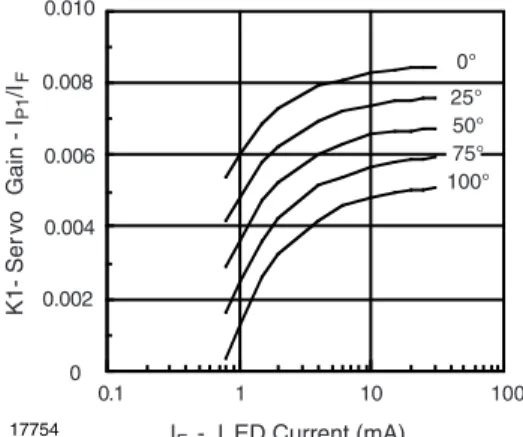
Fig. 5 - Servo Gain vs. LED Current and Temperature
Fig. 6 - Normalized Transfer Gain vs. LED Current and Temperature
Fig. 7 - Amplitude Response vs. Frequency iil300_02 1.4 1.3 1.2 1.1 0 5 10 15 20 25 30 35
VF - LED Forward Voltage (V) IF
- LED Current (mA)
1.0 iil300_04 0 °C 25 °C 50 °C 75 °C 0.1 1 10 100 300 250 200 150 100 50 0
IF - LED Current (mA)
IP1
- Servo Photocurrent (µA)
VD = - 15 V iil300_06 0 10 15 20 25 3.0 2.5 2.0 1.5 1.0 0.5 0.0
IF - LED Current (mA)
Normalized Photocurrent Normalized to: IP1 at IF = 10 mA TA = 25 °C VD = - 15 V 0 °C 25 °C 50 °C 75 °C 5 IF- L ED Current (mA) 0.1 1 10 100 0 K1-Ser v o Gain -IP1 /IF 0.010 0.008 0.006 0.004 0.002 0° 25° 50° 75° 100° 17754 iil300_11 0 10 15 20 25 1.010 1.005 1.000 0.995 0.990
IF - LED Current (mA)
K3 - Transfer Gain - (K2/K1) 0 °C 25 °C 50 °C 75 °C Normalized to: IF = 10 mA TA = 25 °C 5 iil300_12 104 105 106 5 0 - 5 - 10 - 15 - 20 F - Frequency (Hz) Amplitude Response (dB) RL = 1 kΩ IF = 10 mA, Mod = ± 2.0 Ma (peak)
IL300
Vishay Semiconductors
Linear Optocoupler, High Gain
Stability, Wide Bandwidth
Fig. 8 - Amplitude and Phase Response vs. Frequency
Fig. 9 - Common-Mode Rejection
Fig. 10 - Photodiode Junction Capacitance vs. Reverse Voltage
APPLICATION CONSIDERATIONS
In applications such as monitoring the output voltage from a line powered switch mode power supply, measuring bioelectric signals, interfacing to industrial transducers, or making floating current measurements, a galvanically isolated, DC coupled interface is often essential. The IL300 can be used to construct an amplifier that will meet these needs.
The IL300 eliminates the problems of gain nonlinearity and drift induced by time and temperature, by monitoring LED output flux.
A pin photodiode on the input side is optically coupled to the LED and produces a current directly proportional to flux falling on it. This photocurrent, when coupled to an amplifier, provides the servo signal that controls the LED drive current. The LED flux is also coupled to an output PIN photodiode. The output photodiode current can be directly or amplified to satisfy the needs of succeeding circuits.
ISOLATED FEEDBACK AMPLIFIER
The IL300 was designed to be the central element of DC coupled isolation amplifiers. Designing the IL300 into an amplifier that provides a feedback control signal for a line powered switch mode power is quite simple, as the following example will illustrate.
See figure 12 for the basic structure of the switch mode supply using the Infineon TDA4918 push-pull switched power supply control cChip. Line isolation are provided by the high frequency transformer. The voltage monitor isolation will be provided by the IL300.
The isolated amplifier provides the PWM control signal which is derived from the output supply voltage. Figure 13 more closely shows the basic function of the amplifier. The control amplifier consists of a voltage divider and a non-inverting unity gain stage. The TDA4918 data sheet indicates that an input to the control amplifier is a high quality operational amplifier that typically requires a + 3 V signal. Given this information, the amplifier circuit topology shown in figure 14 is selected.
The power supply voltage is scaled by R1 and R2 so that there is + 3 V at the non-inverting input (Va) of U1. This voltage is offset by the voltage developed by photocurrent flowing through R3. This photocurrent is developed by the optical flux created by current flowing through the LED. Thus as the scaled monitor voltage (Va) varies it will cause a change in the LED current necessary to satisfy the differential voltage needed across R3 at the inverting input. The first step in the design procedure is to select the value of R3 given the LED quiescent current (IFq) and the servo gain (K1). For this design, IFq = 12 mA. Figure 4 shows the servo photocurrent at IFq is found to be 100 mA. With this data R3 can be calculated.
iil300_13 dB Phase Ø - Phase Response (°) 103 104 105 106 107 5 0 - 5 - 10 - 15 - 20 45 0 - 45 - 90 - 135 - 180 F - Frequency (Hz) Amplitude Response (dB) IFq = 10 mA Mod = ± 4.0 mA TA = 25 °C RL = 50 Ω iil300_14 - 130 - 120 - 110 - 100 - 90 - 80 - 70 - 60 F - Frequency (Hz) CMRR - Rejection Ratio (dB) 106 101 102 103 104 105 iil300_15 0 2 4 6 8 10 12 14 Voltage (Vdet) Capacitance (pF) 0 2 4 6 8 10 R3 = Vb IPI = 3 V 100 µA = 30 kΩ 17164
IL300
Linear Optocoupler, High Gain
Stability, Wide Bandwidth
Vishay Semiconductors
Fig. 11 - Isolated Control Amplifier
For best input offset compensation at U1, R2 will equal R3. The value of R1 can easily be calculated from the following.
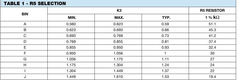
The value of R5 depends upon the IL300 Transfer Gain (K3). K3 is targeted to be a unit gain device, however to minimize the part to part Transfer Gain variation, Infineon offers K3 graded into ± 5 % bins. R5 can determined using the following equation,
or if a unity gain amplifier is being designed (VMONITOR = VOUT, R1 = 0), the equation simplifies to:
Fig. 12 - Switching Mode Power Supply
Fig. 13 - DC Coupled Power Supply Feedback Amplifier
iil300_16 + -Voltage monitor R1 R2 To control input ISO AMP +1
R1 = R2
(
V
MONITORVa
- 1
)
17165R5 =
V
OUTV
MONITOR xR3 (R1 + R2)
R2K3
17166R5 =
R3
K3
17190 iil300_17 Switch Xformer Switch mode regulator TDA4918 Isolated feedback Control 110/ 220 main DC output AC/DC rectifier AC/DC rectifier iil300_18 8 7 6 5 100 pF 4 3 1 2 8 6 7 K1 VCC VCC 1 2 3 4 K2 VCC Vmonitor R1 20 kΩ R2 30 kΩ R3 30 kΩ R4 100 Ω Vout To control input R5 30 kΩ IL300 Vb Va + -U1 LM201IL300
Vishay Semiconductors
Linear Optocoupler, High Gain
Stability, Wide Bandwidth
Table 1. Gives the value of R5 given the production K3 bin.The last step in the design is selecting the LED current limiting resistor (R4). The output of the operational amplifier is targeted to be 50 % of the VCC, or 2.5 V. With an LED quiescent current of 12 mA the typical LED (VF) is 1.3 V. Given this and the operational output voltage, R4 can be calculated.
The circuit was constructed with an LM201 differential operational amplifier using the resistors selected. The amplifier was compensated with a 100 pF capacitor connected between pins 1 and 8.
The DC transfer characteristics are shown in figure 17. The amplifier was designed to have a gain of 0.6 and was measured to be 0.6036. Greater accuracy can be achieved by adding a balancing circuit, and potentiometer in the input divider, or at R5. The circuit shows exceptionally good gain linearity with an RMS error of only 0.0133 % over the input voltage range of 4 V to 6 V in a servo mode; see figure 15.
Fig. 14 - Transfer Gain
Fig. 15 - Linearity Error vs. Input Voltage
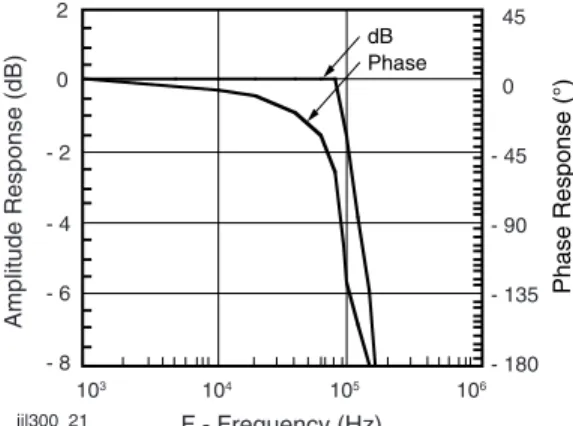
The AC characteristics are also quite impressive offering a - 3 dB bandwidth of 100 kHz, with a - 45° phase shift at 80 kHz as shown in figure 16.
TABLE 1 - R5 SELECTION
BIN
K3 R5 RESISTOR
MIN. MAX. TYP. 1 % kΩ
A 0.560 0.623 0.59 51.1 B 0.623 0.693 0.66 45.3 C 0.693 0.769 0.73 41.2 D 0.769 0.855 0.81 37.4 E 0.855 0.950 0.93 32.4 F 0.950 1.056 1 30 G 1.056 1.175 1.11 27 H 1.175 1.304 1.24 24 I 1.304 1.449 1.37 22 J 1.449 1.610 1.53 19.4
V
opamp- VF
I
Fq=
2.5 V - 1.3 V
12 mA
= 100
Ω
R4 =
17096 iil300_19 6.0 5.5 5.0 4.5 4.0 2.25 2.50 2.75 3.00 3.25 3.50 3.75 Vout - Output Voltage (V) Vout = 14.4 mV + 0.6036 x Vin LM 201 Ta = 25 °C iil300_20 6.0 5.5 5.0 4.5 4.0 - 0.015 - 0.010 - 0.005 0.000 0.005 0.010 0.015 0.020 0.025 Vin - Input Voltage (V) Linearity Error (%) LM201IL300
Linear Optocoupler, High Gain
Stability, Wide Bandwidth
Vishay Semiconductors
Fig. 16 - Amplitude and Phase Power Supply Control
The same procedure can be used to design isolation amplifiers that accept bipolar signals referenced to ground. These amplifiers circuit configurations are shown in figure 17. In order for the amplifier to respond to a signal that swings above and below ground, the LED must be pre biased from a separate source by using a voltage reference source (Vref1). In these designs, R3 can be determined by the following equation.
Fig. 17 - Non-inverting and Inverting Amplifiers iil300_21 dB Phase Phase Response (°) 103 104 105 106 2 0 - 2 - 4 - 6 - 8 45 0 - 45 - 90 - 135 - 180 F - Frequency (Hz)
Amplitude Response (dB)
R3 =
V
ref1I
P1 =V
ref1K1I
Fq 17098 iil300_22 Vcc 20 pF 4 1 2 3 4 8 7 6 5 + Vref2 R5 R6 7 2 4 3 Vo R4 R3 - Vref1 Vin R1 R2 3 7 6 + +Vcc 100Ω 6 IL 300 2 - Vcc - Vcc Vcc - Vcc + Vcc 20 pF 4 1 2 3 4 8 7 6 5 + Vref2 7 2 4 3 Vout R4 R3 + Vref1 Vin R1 R2 3 7 6 + + Vcc 100Ω 6 2 Vcc Vcc - Vcc + Vcc – –Non-inverting input Non-inverting output
Inverting input Inverting output
IL 300
– –
- Vcc Vcc
TABLE 2 - OPTOLINEAR AMPLIEFIERS
AMPLIFIER INPUT OUTPUT GAIN OFFSET
Non-inverting
Inverting Inverting V =OUT K3 R4 R2 VIN R3 (R1 + R2)
Vref1 R4 K3 Vref2 =
R3 Non-inverting Non-inverting V =VOUT K3 R4 R2 (R5 + R6)
IN R3 R5 (R1 + R2)
- Vref1 R4 (R5 + R6) K3 Vref2 =
R3 R6
Inverting
Inverting Non-inverting V =OUT - K3 R4 R2 (R5 + R6) VIN R3 R5 (R1 + R2)
Vref1 R4 (R5 + R6) K3 Vref2 =
R3 R6 Non-inverting Inverting V =OUT - K3 R4 R2
VIN R3 (R1 + R2)
- Vref1 R4 K3 Vref2 =
IL300
Vishay Semiconductors
Linear Optocoupler, High Gain
Stability, Wide Bandwidth
These amplifiers provide either an inverting or non-invertingtransfer gain based upon the type of input and output amplifier. Table 2 shows the various configurations along with the specific transfer gain equations. The offset column refers to the calculation of the output offset or Vref2 necessary to provide a zero voltage output for a zero voltage input. The non-inverting input amplifier requires the use of a bipolar supply, while the inverting input stage can be implemented with single supply operational amplifiers that
permit operation close to ground.
For best results, place a buffer transistor between the LED and output of the operational amplifier when a CMOS opamp is used or the LED IFq drive is targeted to operate beyond 15 mA. Finally the bandwidth is influenced by the magnitude of the closed loop gain of the input and output amplifiers. Best bandwidths result when the amplifier gain is designed for unity.
PACKAGE DIMENSIONS in millimeters
PACKAGE MARKING (this is an example of the IL300-E-X001)
i178010 ISO method A Pin one ID 3 4 10° 1 2 4° 3° 9 6 5 8 7 0.527 0.889 3.302 3.810 0.406 0.508 7.112 8.382 1.016 1.270 9.652 10.16 0.203 0.305 2.794 3.302 6.096 6.604 0.508 ref. 0.254 ref. 0.254 ref. 2.540 1.270 7.62 typ. 8 min. 0.51 1.02 7.62 ref. 9.53 10.03 0.25 typ. 0.102 0.249 15° max. Option 9 0.35 0.25 10.16 10.92 7.8 7.4 10.36 9.96 Option 6 8 min. 7.62 typ. 4.6 4.1 8.4 min. 10.3 max. 0.7 Option 7 18450 21764-41 IL300-E V YWW H 68 X001
Disclaimer
Legal Disclaimer Notice
Vishay
ALL PRODUCT, PRODUCT SPECIFICATIONS AND DATA ARE SUBJECT TO CHANGE WITHOUT NOTICE TO IMPROVE RELIABILITY, FUNCTION OR DESIGN OR OTHERWISE.
Vishay Intertechnology, Inc., its affiliates, agents, and employees, and all persons acting on its or their behalf (collectively, “Vishay”), disclaim any and all liability for any errors, inaccuracies or incompleteness contained in any datasheet or in any other disclosure relating to any product.
Vishay makes no warranty, representation or guarantee regarding the suitability of the products for any particular purpose or the continuing production of any product. To the maximum extent permitted by applicable law, Vishay disclaims (i) any and all liability arising out of the application or use of any product, (ii) any and all liability, including without limitation special, consequential or incidental damages, and (iii) any and all implied warranties, including warranties of fitness for particular purpose, non-infringement and merchantability.
Statements regarding the suitability of products for certain types of applications are based on Vishay’s knowledge of typical requirements that are often placed on Vishay products in generic applications. Such statements are not binding statements about the suitability of products for a particular application. It is the customer’s responsibility to validate that a particular product with the properties described in the product specification is suitable for use in a particular application. Parameters provided in datasheets and/or specifications may vary in different applications and performance may vary over time. All operating parameters, including typical parameters, must be validated for each customer application by the customer’s technical experts. Product specifications do not expand or otherwise modify Vishay’s terms and conditions of purchase, including but not limited to the warranty expressed therein.
Except as expressly indicated in writing, Vishay products are not designed for use in medical, life-saving, or life-sustaining applications or for any other application in which the failure of the Vishay product could result in personal injury or death. Customers using or selling Vishay products not expressly indicated for use in such applications do so at their own risk and agree to fully indemnify and hold Vishay and its distributors harmless from and against any and all claims, liabilities, expenses and damages arising or resulting in connection with such use or sale, including attorneys fees, even if such claim alleges that Vishay or its distributor was negligent regarding the design or manufacture of the part. Please contact authorized Vishay personnel to obtain written terms and conditions regarding products designed for such applications.
No license, express or implied, by estoppel or otherwise, to any intellectual property rights is granted by this document or by any conduct of Vishay. Product names and markings noted herein may be trademarks of their respective owners.