Research Article
a
May
2019
Computer Science and Software Engineering
ISSN: 2277-128X (Volume-9, Issue-5)
Direct Memory Access with Cypress (PSoC) and MATLAB
Manish AggarwalStudent, ECE / Guru Kashi University, Talwandi Sabo, Punjab, India
Email:[email protected]
Dr. Mahendra Kumar
Professor, ECE / Guru Kashi University, Talwandi Sabo, Punjab, India Email: [email protected]
Abstract- Programmable system on Chip are emerging as a powerful solution due to their ease of use and ability to replace large number of discrete ADC / DAC advantage. Simply replacing a large number of discrete components provides a significant power advantage. Here we will give an overview as how to implement an application based on PSOC by using PSOC Developer Kit which provides a common development platform where we can prototype and evaluate different solutions using PSOC architectures. Applications of PSOC are numerous in number and it takes lot of time to arrive at the conclusion especially for the start-ups. We have given the detailed view of the process and point to point description of the work, practices taken by us to achieve the application.
To enhance our basic approach towards the main goal we have started with implementing basic projects i.e. LCD Interfacing Project, Controlling Blinking LEDs and many more projects using the family processors i.e. CY8C28, CY8C38, CY8C55. After all the small projects we have actually focused in detail about achieving the applications. We will read about the “ADC data buffering using DMA” on PSOC. Our application is how to configure direct memory access (DMA) to buffer the analog to digital converter. Also {DMA} design and implementation of scientific calculator through Matrix laboratory.
Keyboard : PSoC-5 board, USB cable, LCD, MATLAB.
I. INTRODUCTION
PSoC microcontroller is plays a very widel role in many applications now a days. As for a project it covers all the needs on a single chip. It gives a whole new concept of microcontroller as it contains both analog & digital blocks. PSoC (Programmable system on chip) is made by Cypress semiconductor & is to be defined as the family of integrated circuits. We will work here on PSoC Designer, PSoC Creator, PSoC Programmer for achieving the results & for further analyzing them.PSoC (Programmable System on Chip) represents a whole new concept in microcontroller development. In addition to all the standard elements of 8-bit microcontrollers, PSoC chips feature digital and analog programmable blocks, which themselves allow implementation of large number of peripherals. Digital blocks consist of smaller programmable blocks that can be configured to allow different development options. Analog blocks are used for development of analog elements, such as analog filters, comparators, instrumentational (non)inverting amplifiers, as well as AD and DA convertors. There’s a number of different PSoC families on which we will work, depending on the project requirements. Basic difference between PSoC families is the number of available programmable blocks and the number of input/output pins. Number of components that can be devised is primarily a function of the available programmable blocks.
II. OBJECTIVE
The main objective of this paper is to make us understand the role of importance of PSoC in our lives and also to know about its various applications. Here we are going to provide a complete report on the functionality and also the implementation of various projects on PSoC. Our main application over which we will work on is direct memory access (DMA) to buffer the analog to digital converter. In case of ADC data buffer we will see the data will buffer easily with less losses.
NEED OF OBJECT
ISSN(E): 2277-128X, ISSN(P): 2277-6451, pp. 68-74 THEORY WORK
PSoC Designer is program package that leads user through all stages of developing project. Here we will study about version 4.2 and version 5.1, but our applications on which we will work on will still remain competent in case of newer versions, because differences are shown only in addition of new programmable components and some minor improvements. The most important for user is to get familiar with two main parts of PSoC Designer:
o Device Editor
o Application Editor
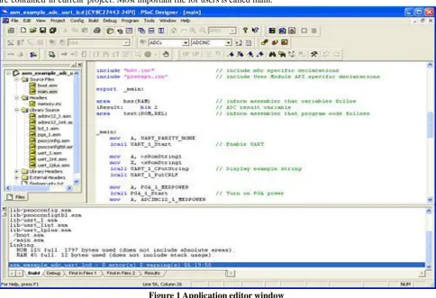
Beside these two, there is also a debugger part, but it demands as an additional hardware. Device editor consists of two windows. First one is for selection of the components and is called as User Module selection View. Other, is called Interconnection View and it is used for setting and connecting components and parameter adjustment. B y clicking on appropriate icon transferring from one to the other part of the PSoC Designer is done easily. Device Editor Icon must be selected first for opening the Interconnection View or User module Select windows. Lower image shows look of the programmable component choice window.
III. APPLICATION EDITOR
Application Editor is used for writing programs, which can be done using assembly or C. Application Editor itself, bears much resemblance to IDE-s of other standard 8-bit microcontrollers. Left side window holds list of files that are contained in current project. Most important file for users is called main.
Figure 1 Application editor window
This is the place of user code start. Include files are generated automatically based on selected programmable blocks in Device Editor, clicking on icon Generate Application. For example, if set programmable blocks are adcinc12, pga, and LCD, PSoC Designer automatically generates files with data and subprograms for their usage. As shown in figure 1.
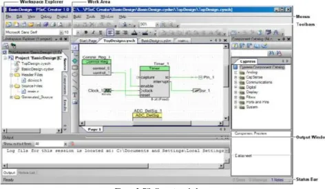
PSoC CREATOR
ISSN(E): 2277-128X, ISSN(P): 2277-6451, pp. 68-74 Workspace – A workspace is the top-level container within PSoC Creator; it contains one or more projects that we can open, close, and save together. We can only have one workspace for any given PSoC Creator workspace file (.cywrk). Project – A project contains multiple items that represent our design, such as schematics, design-wide resources, source code, and hex files. The types of items contained within a project vary according to the project type. A project is always part of a workspace. We can create projects in an existing workspace or we can create a new workspace as part of creating a new project.
A PSoC Creator project contains multiple items, such as schematics, components, design- wide resources, source code, and hex files. PSoC Creator provides two types of projects: design and library.
Design Project – A design project is used to create and modify designs. With a design project, select and configure the components for our device in a schematic. Next, set up design-wide resources, such as clocks and interrupts. Then, write the C code for our application. Finally, we build (and debug) the project to generate the hex file and program the device. When we first create a design project, PSoC Creator creates the project/workspace files and directory structure, as well as the top -level schematic, main.c shell file, a design-wide resources file (.cydwr), and a device.h file.
Library Project – A library project is a collection of one or more components and the associated source code. With a library project, we can develop components that will be elaborated in a design, as well as reused in many designs. Development includes creating the graphic symbol, defining parameters, and specifying validation requirements. When we first create a library project, PSoC Creator creates the project/workspace files and directory structure. Library projects(s) are included in PSoC Creator as Dependencies to determine which components are available for us to designs in the Component Catalog .component is a collection of files, such as a symbol, schematics, APIs, and documentation, that defines functionality within the PSoC Device.
PSoC Creator framework provides numerous features to help organize our designs and complete projects faster. As shown in figure 2.
Figure 2. PSoC creator window
When we first open PSoC Creator, the framework displays with a Workspace Explorer, document work area, and Output window. The framework also contains a menu and a status bar, as well as various toolbars that will change depending on the type of file.
IV. METHODEOLOGY
ISSN(E): 2277-128X, ISSN(P): 2277-6451, pp. 68-74 Secondly we will be implementing a project which demonstrates a 9-bit Delta Sigma ADC by measuring the voltage of the potentiometer center tap wiper and displaying the result on the LCD on all the processor modules and all the software. These all were the basic projects that we done for knowing the steps for performing the applications. These basic projects that we done helps us for getting our main applications.
After doing all these minor projects we comes to know about the usage of the PSoC we will directly focus on achieving the applications of PSoC. In case of ADC data buffering using DMA , DMA controller is uses in both PSoC3 & PSoC5 software & it is uses to handle the data transfer without CPU intervention. DMA is useful in applications that require ADC data buffering and allows the CPU for doing the simultaneous tasks. Here we will see the basics of 8-bit, 16-8-bit, and 20-bit Delta Sigma ADC data buffering using DMA with example projects. The 20-bit example project accompanying this application note demonstrates problems with data buffering using DMA. These problems occur when the peripheral spoke width is less than the actual data width. The project describes how to tackle this using multiple DMA channels.
The DMA is used to move data from a source to destination without CPU intervention is the basic concept on which we will further work. In our third application i.e. USB HID intermediate with Keyboard, We are using here PSoC's full speed USB interface, where we will take the basics of USB HID development and its implementation is depends upon the knowledge by which users get knows that how to incorporate the OUTPUT items to receive information from a host device using the status LEDs on a keyboard taking as an example, we also send the keyboard information as an INPUT to type a predefined string of text into a text editor.
We have used the software development kit to perform various tasks and they are described below as:
V. PSOC DEVELOPMENT KIT
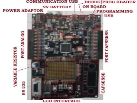
Figure 3. PSoC Development Kit
The CY8CKIT-001 PSoC Development Kit (DVK) is the kit that provides us a common development platform where we can prototype and evaluate different solutions using any one of the PSoC 1, PSoC 3, or PSoC 5 architectures. This is the kit that provide us a practical understanding of PSoC technology. In addition of this the kit also includes several example projects with step -by-step instructions to enable us to easily get started developing PSoC solutions. This kit includes PSoC 1, PSoC 3, and PSoC 5 Family Processor Modules. PSoC Development Board is to be shown as in figure 3.
.
ISSN(E): 2277-128X, ISSN(P): 2277-6451, pp. 68-74 The CY8CKIT-001 PSoC Development Board is designed to aid hardware, firmware, and software developers in building their own systems around Cypress’s PSoC devices. One of the main big feature of this board that it provides the flexibility to configure the power domains. To the board Input power is from one of two sources:
12V 1A power supply adapter
9V battery (not included)
This is the full featured board incorporates three onboard linear regulators that power peripherals and PSoC processor modules at voltages between 1.7V and 5.0V. These regulators include a fixed 5V 1A linear regulator, a fixed 3.3V 300 mA linear regulator, and a 1.5V to 5.5V 300 mA adjustable regulators. The board also provides the ability to separate the PSoC core VDD rail into two separate rails, analog and digital.
The board was designed with modularity in mind and, as a result, supports removable processor modules. This is the parameter which allows us to plug the different PSoC processor modules into the board based upon the desired features of both 8-bit and 32-bit PSoC devices.
The PSoC CY8C28 Family Processor Module is designed to evaluate and experiment with Cypress’s PSoC programmable system-on-chip in designing methodology and architecture. This processor module can be used in conjunction with the PSoC Development Kit (CY8CKIT-005) to create designs utilizing on-board resources or compatible expansion boards. This kit also provides us with an additional processor module to use with different projects
DEBUG
The MiniProg is a protocol translation device. It enables PC host software to communicate through high speed USB to the target device to be programmed or debugged. The device side communication protocol can be one of several standards; this can occur ove r either use of 5-pin or 10-pin connectors. MiniProg enables the communication with target devices using I/O voltage levels from 1.5V to 5.5V.MiniProg3 can provide power to a simple target board, at one of four voltage levels. Program/Debug Ribbon Cable and It is used to connect miniProg3 to the processor modules in case of CY8C55 and CY8C38 Family Processor Modules. USB Cable and It is used to connect miniProg3 to the PC/laptop.
12V AC Power Adapter. The input power to the board is from 12V AC Power Adapter Quick Start Guide and It gives the detailed description of the kit and several programmes and applications to be implemented on the kit.
Kit CDs, which includes: PSoC Creator, PSoC Designer, PSoC Programmer, Projects, and Documentation. It includes the original software i.e. Creator, programmer and designer to get installed easily on the computer/laptop. It also contains the programmes and documentation related to the different processor modules.
VI. RESULT ANALYSIS
In this research paper we have shown the simulation results obtained by us while working on different applications of the PSoC. 1) ADC Data buffering using DMA 2) Direct memory access based design and implementation scientific calculator using MATLAB.
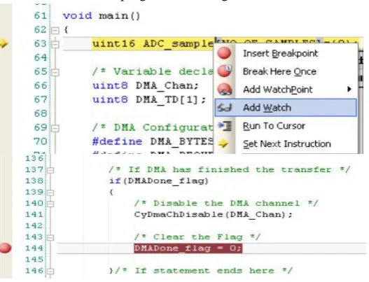
1. ADC DATA BUFFERING USING DMA Build and program the chip
-Press F5 or click the debug icon to download the program and debug.
ISSN(E): 2277-128X, ISSN(P): 2277-6451, pp. 68-74 The execution stops at the breakpoint after the DMA transfers the specified number of samples from ADC to memory and the result can be verified by monitoring the “ADC_sample” array in the watch window. The outputs for 8 bit, 16 bit,20 bit and 12 bit ADC SAR as follows. As shown in figure 5 & 6.
Figure 6 Direct memory access (DMA) to buffer the analog to digital converter
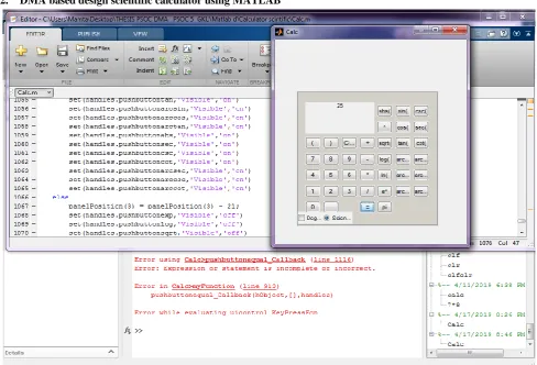
2. DMA based design scientific calculator using MATLAB
Figure 7. scientific calculator using MATLAB
VII. CONCLUSION
ISSN(E): 2277-128X, ISSN(P): 2277-6451, pp. 68-74 REFRENCES
[1] Anu MD,Lakshmi Natarajan , CY8C38xx/CY8C55xx on software version of PsoC Creator for PSoC 3 &
PSoC 5-“Getting Started with DMA”.
[2] Using DMA with high performance peripherals to Maximize the system performance by John Manjine.
[3] Anu MD,Anup Mohan “PSoC 3 & PSoC for ADC data Buffering using DMA”.
[4] USB HID intermediate with Keyboard using CY8C38xx, CY8C55xx on PSoC 3/PSoC 5 by Robert Murphy.
[5] Robert Murphy “PSoC 3 & PSoC 5 for USB Fundamentals”.
[6] RtrASSoc: an adaptable superscalar reconfigurable system-on-chip.
[7] The Method of data exchange between high performance PWM modulator and MCU by Maxim, D. ; Volkov,
A.G. ; Makarov, D.V. Micro/Nanotechnologies and Electron Devices (EDM), 2012 IEEE 13th International Conference Publication Year: 2012.
[8] A human-robot interface using vision-based eye gaze estimation system Dong Hyun Yoo ; Jae Heon Kim ; Do