Please cite this article as:M. A. Javadi Rad, A. Taheri, Digital Controller Design based on Time Domain for DC-DC Buck Converter, International Journal of Engineering (IJE), TRANSACTIONS B: Applications Vol. 28, No. 5, (May 2015) 693-700
International Journal of Engineering
J o u r n a l H o m e p a g e : w w w . i j e . i rDigital Controller Design based on Time Domain for DC-DC Buck Converter
M. A. Javadi Rad*, A. Taheri
Department of Electrical Engineering, University of Zanjan
P A P E R I N F O
Paper history:
Received 27 February 2014
Received in revised form 09 March 2015 Accepted 04 April 2015
Keywords:
DC-DC Buck Converter Digital PID Controller Integral Square Error (ISE) Patterning
State-space Averaged (SSA) Voltage Mode Control
A B S T R A C T
In this paper, the digital controller design for compensating the dc-dc buck converter output voltage has been analyzed in the digital domain. The main idea of this paper is patterning the samples of high order ideal controller and using integral square error in determining digital PID coefficients. This approach provides higher precision of digital controller design and eliminates the need for manipulating the coefficients, which in turn will lead to stringent design parameters in response to the system output. The proposed scheme has been simulated in MATLAB software and the results have been presented. The digital controller has been designed based on the proposed method for the buck converter and has been implemented on a TMS320LF2812 DSP core.
doi: 10.5829/idosi.ije.2015.28.05b.07
1. INTRODUCTION1
In recent years, DC–DC converters with step-up/step-down characteristics have been widely used in applications such as portable devices [1-4], communication power supply [5, 6], power factor correction [7-11], hybrid electrical vehicles or fuel-cell vehicles [12, 13].
The design of DC–DC converter controllers has experienced considerable changes during the recent decades. Considering many advantages offered by digital control over the analog control, abundant attention has been devoted to the digital control [14]. These advantages include stable functioning, flexibility and capability in implementation of complex control algorithms. There exist numerous methods for controller design in digital control, e.g. designing the controller in frequency domain and thereafter transferring it to the digital domain [15, 16].
PID controllers are one of the most widely used controllers in the industry [17], to the extent that they are used in more than 90% of modern industrial
1*Corresponding Author’s Email: [email protected](M. A.
Javadi Rad)
processes. The reason for this popularity lies in the simplicity, versatility, speed, reliability and flexibility which this controller offers. A variety of methods and formulae have been introduced so far for adjustment of the PID controller, the most important of which to mention include the Ziegler and Nichols [18] and Cohen and Coon [19] methods. In 1991 new settings were introduced for the Ziegler and Nichols method [20]. The method was based on particle swarm optimization (PSO) algorithm [21]. The Internal Model Control designing method and Integral of Time Absolute Value minimization method [22] have also been introduced for regulating the controller. In most of the introduced methods for maximum yield, the optimized value is reached after designing the controller coefficients and mathematical manipulation [23].
The main idea of this paper is patterning the samples of high order ideal controller and using integral square error in determining digital PID coefficients. Accurate designing of digital controller and no requirement for mathematical manipulation are from the privileges of the proposed method, resulting in careful fulfillment of the design parameters in system output response.
In this paper, initially a sample buck converter has been considered and the small signal transfer function in
the frequency domain has been obtained using the State-Space Averaged model. In the next stage, the open-loop response of the converter in the digital domain has been determined with the aid of one of the S-Z domain transformations. Afterwards, considering the design parameters and using Truxal rules [24] and one of the S-Z domain transformations, the ideal closed-loop response was specified in the digital domain. Considering the open and closed-loop response of the system, the high order ideal digital controller was designed. Then by patterning the ideal controller behavior and minimization of integral square error, the digital PID controller parameters are designed. Finally the buck converter was simulated in MATLAB software considering the load changes and compensated for the purpose of regulating the output voltage. The simulation and implementation output results confirmed the efficiency of the proposed method.
The paper structure is as follows: use of the State-Space Averaged model, determination of small signal transfer function of the converter and the proposed method for digital controller design have been presented in the section 2; in section 3, a digital controller will be designed for a DC-DC buck converter based on the introduced method. The performance comparison of the controllers designed for DC-DC converter are made in section 4. Section 5 includes the implementation results. Finally, the conclusion will be given in section 6.
2. DIGITAL CONTROLLER DESIGN SCHEME
2. 1. State-space Averaged Model for DC-DC Buck
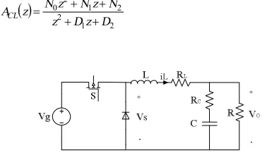
Converter Figure 1 illustrates the circuit structure
of a buck converter.
The small signal transfer function of the buck converter is obtained through different methods [25, 26]. To achieve this goal, the State-Space Averaged technique has been used:
In this equation, vˆo and dˆ are the small variations of
the output voltage and duty cycle, respectively.
2. 2. Proposed Method for Digital Controller
Design The proposed method in this paper is based
on patterning of the samples of high order ideal controller and using integral square error in determining digital PID coefficients. This approach provides increased accuracy in designing of digital controller and no requirement for manipulation of coefficients leading to careful fulfillment of the design parameters in system output response. At first, considering the design
parameters including the maximum overshoot and settling time values, the denominator coefficients of ideal closed-loop response in frequency domain are obtained. In a general sense, the standard form of a second-order system can be described using the relationship (2):
It is important to note that the Fs numerator is not necessarily equal to wn2. In this relationship,wn is the
angular frequency and z is the damping ratio. Considering the design valuests (settling time) and MP
(maximum overshoot) and their relationship with z and
n
w , the denominator Fs can be determined. The
relationships between tsand MPwith z and wn have been presented below:
Using these two relationships and the known amounts
s
t and MP the z and wn values are obtained. After determining the denominator of the relationship (2), the equation is transferred to the digital domain with the help of one of the S-Z transformations (e.g. zero order hold) and the denominator of closed-loop response is determined in the digital domain. Then it is normalized using the greatest exponent coefficient [27]:
The closed-loop form of the transfer function in the digital domain is as follows. It should be noted that the numerator order should not be greater than the denominator order.
Figure 1. DC-DC buck converter ( )
( )
[
]
( )÷÷ ø ö çç è æ
+ + + ÷÷ ø ö çç
è æ
+ + + +
+ =
L C L
L C
C g o
R R
R R LC s R R
L C R R C R s
C sR V s
d s v
2
1
1 ˆ
ˆ
(1)
2 2
2
2 n n
n s
s F
w zw
w + +
= (2)
2
1z zp
-=e
MP (3)
n s
t
zw
4
= (4)
2 1 2
0z dz d
d
denF = + + (5)
2 1
2 Dz D
z
DENF = + + (6)
0 1 1 d
d
D =
0 2
2 dd
D = (7)
( )
2 1
2 1 2
2 0
D z D z
N z N z N z ACL
+ +
+ +
The N0 , N1 and N2 coefficients are obtained
considering the Truxal rule set. The mentioned rule set is as follows:
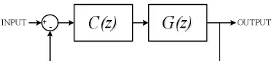
In the next step, the open-loop response of the system shown in section 2.1 is transferred from the S domain to the digital domain. Using one of the S to Z transformations, the open-loop response of the system in the digital domain is also determined. Considering the block diagram of a feedback system (Figure 2) the output-input relationships are defined as follows:
The C
( )
z block is the controller of the system which is determined using Equation (13) as follows.Using this relationship, the ideal digital controller for the digital domain is designed. The high number of zeros and the pole Cideal
( )
z could cause theimplementation of the controller costly and time consuming. To remove this problem, a controller with lower order compared with Cideal
( )
z and a behaviorsimilar to Cideal
( )
z should be designed. The PID analogformat in general state is expressed using the formula (14):
There have been various kinds of methods to nail to discrete PID model like backward difference, forward difference, bilinear transformation, impulse-invariance, step invariance and matched pole-zero. The discrete form of PID through backward difference method is:
After transferring of Equation (15) to the digital domain and generalization, the following relationships are resulted:
c
S is considered as the ideal controller step response andSe is regarded as the step input. By entering different values into the equation for different times, the unknown coefficients b1, b2, b3can be obtained. If b1,
2
b , b3 coefficients are determined considering the ideal controller behavior, a good approximation of the ideal controller will be achieved. For gaining the b1and b2
values, the first two ideal controller step response are used. The complementary idea of this method is that in order to determine b3 there is a sample in the ideal controller response that causes the controller coefficients to be designed fully optimized. To identify this sample, the minimum integral error value (18) has been used. The error between the output ideal step response and the controlled output step response is considered as the signal error.
For identifying the desired sample, a search space of the ideal controller step has been considered. To limit the search space, only the m of the first sample is used. Numerous experiments proved that m is the sample for which the ideal closed-loop response has maximum overshoot. Considering the samples after m can cause intensive fluctuation of the closed-loop response.
3. DESIGNING OF A SAMPLE CONTROLLER IN DIGITAL DOMAIN
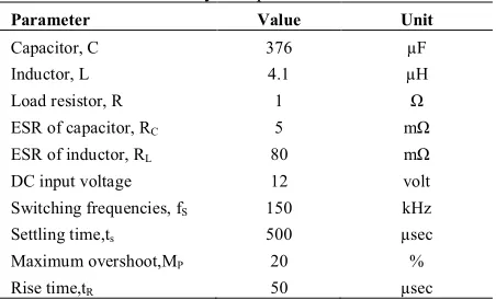
The DC-DC buck converter parameters' values have been given in Table 1.
Figure 2. Basic block diagram of a feedback system.
( )
z=¥ =0CL z
A (9)
( )
z=1=1CL z A (10)
( )
V z CL K dz z dA 1 1= = (11) ( ) ( ) ( )( ) ( ) z C z G z C z G z ACL = +1 (12) ( ) ( ( )( )) ( ) z G z A z A z C CL CL
ideal = 1- (13)
( )= ( )+
ò
( ) + ( )dt t ds K dt t s K t s K t
s D e
e I e P c (14) ( ) ( )( ) ( ) z T z K z z T K K z S z S z C S D S I P e c design 1 1 -+ -+ = = (15) [ ] [ ] [ ]
[ 1] [ 2]
2 1 -+ -÷÷ ø ö çç è æ -+ ÷÷ ø ö çç è æ + + + = + n S T K n S T K K n S T K T K K n S n S e S D e S D P e S D S I P c c (16) ÷÷ ø ö çç è æ + + = S D S I P T K T K K
b1 ÷÷
ø ö çç
è æ- -= S D P T K K
b2 2 ÷÷
ø ö çç è æ = S D T K
b3 (17)
[ ]
n S[ ]
n S[ ]
n errord
ACL ACL
-=
( )
t error[ ]
nTSerror = ISE=
ò
¥e ( )tdt0
2 (18)
0 =
n Sc
[ ]
1=b1 (19)1 =
n Sc
[ ] [ ]
2=Sc1+b1+b2 (20)m n£ £
TABLE 1. System parameter values
Parameter Value Unit
Capacitor, C 376 µF
Inductor, L 4.1 µH
Load resistor, R 1 Ω
ESR of capacitor, RC 5 mΩ
ESR of inductor, RL 80 mΩ
DC input voltage 12 volt
Switching frequencies, fS 150 kHz
Settling time,ts 500 µsec
Maximum overshoot,MP 20 %
Rise time,tR 50 µsec
Using the State-Space Averaged model, the open-loop response of the buck converter small signal is shown in the Relationship (22).
Now, with the help of one of the S-Z transformations, the open-loop response of the system's small signal is mapped into the digital domain. For this purpose, the ZOH transformation has been used:
The value of tsand MP have been considered according to Table 1. The closed-loop response is obtained as given below:
Albeit, it should be noted that all the S-Z domain transformations contain errors. Using the system open-loop response and the closed-open-loop response in Z-domain, the Cideal
( )
z can be determined with the aid of Relationship (13).Considering the ideal controller step response (Figure 3) and the Relationships (19) and (20), the PID parameters have been calculated.
Given Section 2. 2 calculation results, the search space for specifying the b3 value is constructed considering 32 samples (m=32). The maximum overshoot of ideal closed-loop step response has occurred in the sample no. 32. Figure 4 illustrates the integral square errors. The graph holding the lowest area with the time axis is the result of the optimized controller. Here the sample no. 17 has been selected for making the b3 coefficient.
The designed digital controller is therefore resulted as follows:
Considering Figure 5, it can be observed that response of Cideal
( )
z and Cdesign( )
z steps have values very closeto each other. Response of the controlled closed-loop step by the controllers that are different in b3value has been presented in the Figure 6.
Figure 7 shows the controlled closed-loop step response by Cideal
( )
z and Cdesign( )
z . The designparameters' values in ACLd(z) are confirmed. As can be seen from above, the closed-loop response obtained from the designed controller is similar to the ideal closed-loop response with good approximation.
4. PERFORMANCE COMPARISON OF VARIOUS METHODES
The performance comparison of the controllers designed for DC-DC converter are made in over shoot, rise time and settling time.
a: Ideal response with ideal controller b: Internal Mode Control method (IMC) c: Ziegler and Nicholes method (ZN) d: Proposed method
In methods b and c, the controller is designed in the frequency domain and then by Bilinear transform is converted to the digital domain. Since all methods of s to z transmission have some error, the error will influence on parameters of designed controller (b and c). In the proposed method, the controller is designed from the outset in the digital domain, so this error is minimized. As can be seen in Figure 8, closest to the ideal closed-loop response is achieved by the proposed method.
Figure 3. Step response of the buck converter ideal controller.
0 0.1 0.2 0.3 0.4 0.5 0.6 0.7 0.8 0.9 1 x 10⁻⁴ 0 0.1 0.2 0.3 0.4 0.5 0.6 0.7 0.8 0.9
1 S tep Response
Time (s ec onds)
A m p lit ude Cideal ( )
(
)
1 10 4975 . 5 10 503 . 1 1 10 3 . 0 20 5 2 7 4 + ´ + ´ + ´ = - - -s s s s G (22) ( ) 9985 . 0 998 . 1 01489 . 0 01702 . 02- +
-= z z z z G (23) ( ) 4933 . 0 401 . 1 4148 . 0 5067 . 0
2- +
-= z z z z
ACL (24)
( ) 4508 . 0 6076 . 0 4039 . 0 1061 . 0 975 . 2 572 . 3 133 . 2 5067 . 0 2 3 2 3 -+ -+ -= z z z z z z z
Cideal (25)
7055 . 0
1=
b b2=-1.3210b3=0.6294 (26)
( ) 11 2
1 6294 . 0 3210 . 1 7055 . 0 -+ -= z z z z
Table 2 gives the details about the close loop step response of buck converter with different PIDs designed based on b, c and d methods. As seen in Table 2, the design parameters value of the proposed method is much more accurate than the other two methods.
TABLE 2. Closed-loop step responses detail
Method Mp (%) ts (µsec) tr(µsec)
Ideal controller 20 500 50
IMC 22 870 67
ZN 5 535 85
Proposed method 20 545 54
Figure 4. ISE curves between step response of ACL(z) and )
(z ACLd .
Figure 5. Step response of Cideal( )z and Cdesign( )z
Figure 6. Comparison among step responses of controlled systems for any designed controller.
Figure 7. Closed-loop step responses of a system controlled by Cideal
( )
z and Cdesign( )z .Figure 8. Comparison of closed-loop step response of various methods
Figure 9. Voltage-mode pulse width modulation control structure.
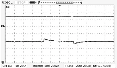
Figure 10. Channel 1: Input voltage (Vg=10volt), Channel 2: output voltage response when the load increased 100% then decreased 50%.
0 0.5 1 1.5 2 2.5 3 3.5 4 4.5 x 10⁻⁴ 0
0.02 0.04 0.06 0.08 0.1 0.12 0.14 0.16 0.18
Time(sec )
A
m
p
lit
ude
0 0.1 0.2 0.3 0.4 0.5 0.6 0.7 0.8 0.9 1 x 10⁻⁴ 0
0.1 0.2 0.3 0.4 0.5 0.6 0.7 0.8 0.9
1 Step Response
Time (seconds)
A
m
p
lit
ude
Cideal Cpid
0 1 2 3 4 5 6 7 8 9
x 10-4
0.6 0.7 0.8 0.9 1 1.1 1.2 1.3
S tep Res ponse
Time (s ec onds)
A
m
p
lit
ude
0 1 2 3 4 5 6 7 8 9
x 10-4 0
0.2 0.4 0.6 0.8 1 1.2
S tep Response
Time (s ec onds)
A
m
p
lit
ude
A cl A cld
0 1 2 3 4 5 6 7 8
x 10-4
0 0.2 0.4 0.6 0.8 1 1.2
Step Response
Time (seconds)
A
m
p
lit
ude
Figure 11. Channel 1: Input voltage (Vg=12volt), Channel 2: output voltage response when the load increased 100% then decreased 50%.
Figure 12. Channel 1: Input voltage (Vg=14volt), Channel 2: output voltage response when the load increased 100% then decreased 50%.
Figure 13. A fabricated DC-DC buck converter and TI C2000 ezdsp F2812.
5. EXPERIMENTAL RESULTS
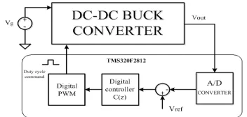
In this paper, the digital control for DC-DC buck converter in voltage mode has been implemented based on the TMS320F2812 digital signal processor chip while its structure is given in Figure 9.
Procedurally, output voltage of DC-DC buck converter is compared with a reference voltage, and then error signal is produced. Indeed, there is a little time which is wasted between error signal sampling and command signal (DC) updating. The PID controllers have been implemented and evaluated using a Texas Instruments (TI) eZdsp F2812 . The eZdsp F2812 is a stand- alone evaluation module with a TMS320F2812 DSP, which is a 32-bit fixed point DSP controller with
on-board flash memory. The CPU operates at 150 MHz. The TMS320F2812 supports peripherals used for embedded control applications, such as event manager modules and a dual 12-bit, 16 channels ADC. The conversion period of the A/D is 80 ns.
The buck converter input voltage in Figure 10, 11 and 12 is 10, 12 and 13 volts, respectively (Channel 1). Channel 2 shows the implemented buck converter output voltage in load changes. The load is initially increased by 100% and then is decreased by 50%. The maximum ripple amplitude is equal to 60 mV. Figure 13 represents the implemented buck converter together with the TI ezdsp F2812 chip.
6. CONCLUSION
In this paper, a new method has been introduced for designing of a digital controller for buck DC-DC converter in digital domain. The proposed method determines the digital controller coefficients with high accuracy. The controller coefficients are determined using primary samples of ideal controller step response. It is important to note that in case the primary samples of ideal controller step response entails negative and non-linear slop, i.e. the ideal controller step response includes initially an undershoot, a step will be added to the proposed method. In this step, considering the behavior of the samples having positive slope, the primary samples are approximated with the same positive slope and then the introduced method is used for determining the digital controller coefficients. Because using the samples with negative slope for determining the digital controller coefficients results in instability of the closed-loop response of the system.
7. ACKNOWLEDGEMENTS
I would like to thank Dr. Asghar Taheri for his most support and encouragement. This research was supported by University of Zanjan.
8. REFERENCES
1. Sahu, B. and Rincon-Mora, G.A., "A low voltage, dynamic, noninverting, synchronous buck-boost converter for portable applications", Power Electronics, IEEE Transactions on, Vol. 19, No. 2, (2004), 443-452.
2. Chakraborty, A., Khaligh, A. and Emadi, A ." Combination of , buck and boost modes to minimize transients in the output of a positive buck-boost converter", in IEEE Industrial Electronics, IECON 2006-32nd Annual Conference on, IEEE, (2006), 2372-2377.
Electronics, IEEE Transactions on, Vol. 24, No. 5, (2009), 1267-1279.
4. Huang, P.-C., Wu ,W.-Q., Ho, H.-H. and Chen, K.-H., "Hybrid buck–boost feedforward and reduced average inductor current techniques in fast line transient and high-efficiency buck–boost converter", Power Electronics, IEEE Transactions on, Vol. 25, No. 3, (2010), 719-730.
5. Ren, X., Ruan, X., Qian, H., Li, M. and Chen, Q., "Dual-edge modulated four-switch buck-boost converter", in Power Electronics Specialists Conference, 2008, PESC 2008. IEEE, (2008), 3635-3641.
6. Ren, X., Tang, Z., Ruan, X., Wei ,J. and Hua, G., "Four switch buck-boost converter for telecom DC-DC power supply applications", in Applied Power Electronics Conference and Exposition, 2008. APEC 2008. Twenty-Third Annual IEEE, IEEE, (2008), 1527-1530.
7. Chen, J., Maksimovic, D. and Erickson, R.W., "Analysis and design of a low-stress buck-boost converter in universal-input pfc applications", Power Electronics, IEEE Transactions on, Vol. 21, No. 2, (2006), 320-329.
8. Andersen, G.K. and Blaabjerg, F., "Current programmed control of a single-phase two-switch buck-boost power factor correction circuit", Industrial Electronics, IEEE Transactions on, Vol. 53, No. 1, (2006), 263-271.
9. Abramovitz, A. and Smedley, K.M., "Analysis and design of a tapped-inductor buck–boostpfc rectifier with low bus voltage",
Power Electronics, IEEE Transactions on, Vol. 26, No. 9,
(2011), 2637-2649.
10. Bortis, D., Waffler, S., Biela, J. and Kolar, J.W., "25-kw three-phase unity power factor buck–boost rectifier with wide input and output range for pulse load applications", Plasma Science,
IEEE Transactions on, Vol. 36, No. 5, (2008), 2747-2752.
11. Sarvi, M. and Abedi, S., "An intelligent algorithm based controller for multiple output DC-DC converters with voltage mode weighting factor " ,International Journal of
Engineering-Transactions C: Aspects, Vol. 27, No. 6, (2013), 889-898.
12. Qiao, H., Zhang, Y., Yao, Y. and Wei, L., "Analysis of buck-boost converters for fuel cell electric vehicles", in Vehicular Electronics and Safety, 2006. ICVES 2006. IEEE International Conference on, IEEE, (2006), 109-113.
13. Waffler, S. and Kolar, J.W., "A novel low-loss modulation strategy for high-power bidirectional buck boost converters",
Power Electronics, IEEE Transactions on, Vol ,٢۴ .No. 6,
(2009), 1589-1599.
14. Duan, Y. and Jin, K., "Digital controller design for switchmode power converters", in Applied Power Electronics Conference and Exposition, 1999. APEC'99. Fourteenth Annual, IEEE. Vol. 2, (1999), 967-973.
15. Liu, Y.-F., Meyer, E. and Liu, X., "Recent developments in digital control strategies for DC/DC switching power converters", Power Electronics, IEEE Transactions on, Vol. 24, No. 11, (2009), 2567-2577.
16. Guo, L., "Implementation of digital pid controllers for DC-DC converters using digital signal processors", in Electro/Information Technology, 2007 IEEE International Conference on, IEEE, (2007), 306-311.
17. Babu, R., Samuel, R., Deepa, S. and Jothivel, S., "A closed loop control of quadratic boost converter using pid-controller",
International Journal of Engineering, Vol. 27, No. 11, (2014),
1653-1662.
18. Ziegler, J.G. and Nichols, N.B., "Optimum settings for automatic controllers", Trans. ASME, Vol. 64, No. 11, (1942). 19. Cohen, G .and Coon, G., "Theoretical consideration of retarded
control", Trans. ASME, Vol. 75, No. 1, (1953), 827-834. 20. Hang, C.C., Astrom, K.J. and Ho, W.K., "Refinements of the
ziegler–nichols tuning formula", in IEE Proceedings D (Control Theory and Applications), IET. Vol. 138, (1991), 111-118. 21. Sarvi, M., Derakhshan, M. and Sedighizadeh, M., "A new
intelligent controller for parallel DC/DC converters",
International Journal of Engineering-Transactions A: Basics,
Vol. 27, No. 1, (2013), 131-142.
22. O'Dwyer, A., "PI and PID controller tuning rule design for processes with delay, to achieve constant gain and phase margins for all values of delay",in Proceedings of the Irish Signals and Systems Conference, NUI Maynooth, Ireland,(2001), 96-101.
23. Peretz, M.M. and Ben-Yaakov, S., "Time-domain design of digital compensators for pwm dc-dc converters", Power
Electronics, IEEE Transactions on, Vol. 27, No. 1, (2012),
284-293.
24. Truxal, J.G. and Weinberg, L., "Automatic feedback control system synthesis", Physics Today, Vol. 8, No. 8, (2009), 17-18. 25. Van de Sype, D.M . , De Gusseme, K., Van den Bossche, A.P.
and Melkebeek, J.A., "Small-signal z-domain analysis of digitally controlled converters", in Power Electronics Specialists Conference, 2004. PESC 04. 2004 IEEE 35th Annual, IEEE, Vol. 6, (2004), 4299-4305.
26. Maksimovic, D. and Zane, R., "Small-signal discrete-time modeling of digitally controlled pwm converters", Power
Electronics, IEEE Transactions on, Vol. 22, No. 6, (2007),
2552-2556.
Digital Controller Design based on Time Domain for DC-DC Buck Converter
M. A. Javadi Rad, A. Taheri
Department of Electrical Engineering, University of Zanjan
P A P E R I N F O
Paper history:
Received 27 February 2014
Received in revised form 09 March 2015 Accepted 04 April 2015
Keywords:
DC-DC Buck Converter Digital PID Controller Integral Square Error (ISE) Patterning
State-space Averaged (SSA) Voltage Mode Control
هﺪﯿﮑﭼ
هزﻮﺣردكﺎﺑلﺪﺒﻣﯽﺟوﺮﺧژﺎﺘﻟويزﺎﺳناﺮﺒﺟرﻮﻈﻨﻣﻪﺑلﺎﺘﯿﺠﯾدﺮﻟﺮﺘﻨﮐﯽﺣاﺮﻃﻪﻟﺎﻘﻣﻦﯾارد
Z
ﺖﺳاهﺪﯾدﺮﮔﺰﯿﻟﺎﻧآ
.
هﺪﯾا
ﺿﻦﯿﯿﻌﺗردﺎﻄﺧﻊﺑﺮﻣلاﺮﮕﺘﻧازاهدﺎﻔﺘﺳاوﻻﺎﺑﻪﺒﺗﺮﻣلآهﺪﯾاﺮﻟﺮﺘﻨﮐيﺎﻫﻪﻧﻮﻤﻧزايرادﺮﺑﻮﮕﻟا،ﻪﻟﺎﻘﻣﻦﯾاردﯽﻠﺻا
ﺐﯾاﺮ
PID
ﺖﺳالﺎﺘﯿﺠﯾد
.
ﯽﻣﻪﺋاراارﺐﯾاﺮﺿيرﺎﮑﺘﺳدﻪﺑزﺎﯿﻧمﺪﻋو لﺎﺘﯿﺠﯾدﺮﻟﺮﺘﻨﮐﯽﺣاﺮﻃردﺖﻗدﺶﯾاﺰﻓا،دﺮﮑﯾورﻦﯾا
ﺪﻨﮐ
دﻮﺷﯽﻣﻢﺘﺴﯿﺳﯽﺟوﺮﺧﺦﺳﺎﭘردﯽﺣاﺮﻃيﺎﻫﺮﺘﻣارﺎﭘﻖﯿﻗدنﺪﺷ هدروآﺮﺑﻪﺑ ﺮﺠﻨﻣﻪﮐ
.
ﻪﯿﺒﺷﺐﻠﺘﻣرديدﺎﻬﻨﺸﯿﭘحﺮﻃ
ﺖﺳاهﺪﯾدﺮﮔﻪﺋاراﺞﯾﺎﺘﻧوهﺪﺷيزﺎﺳ
.
ﺮﻟﺮﺘﻨﮐ
لﺪﺒﻣياﺮﺑهﺪﺷﻪﺋاراشورسﺎﺳاﺮﺑلﺎﺘﺠﯾد
BUCK
وهﺪﯾدﺮﮔﯽﺣاﺮﻃ
ﻪﺘﺴﻫ يور
TMS320LF2812 DSP
ﺖﺳاهﺪﺷيزﺎﺳهدﺎﯿﭘ
. doi: 10.5829/idosi.ije.2015.28.05b.07