JNS 3 (2013) 309-313
Optimization of Sensitivity and Stability of Gold/Silver bi-Layer
Thin Films Used in Surface Plasmon Resonance Chips
M. Ghorbanpour
Chemical Engineering Department, University of Mohaghegh Ardabili, 56199-11367, Ardabil, Iran.
Abstract
The aim of this study is experimental assay of sensitivity and stability of a bimetallic silver/gold SPR sensor chip. This chip utilizes the sensitivity of the silver and the stability of the gold. Moreover, the Silver layer (instead of usual Cr or Ti layer) was used as an adhesive intermediate layer between the Gold layer and the glass substrate. The optimization of the Gold/Silver thickness using SPR analysis and physical and chemical stability tests showed that the 20/30 gold/silver composite resulting in a better precision and more stable SPR sensing chip.
2013 JNS All rights reserved
Article history:
Received 27/9/2013 Accepted 22/11/2013 Published online 1/12/2013
Keywords:
Surface plasmon resonance Sensitivity
Stability
Gold/silver bi-layer film
Corresponding author: E-mail address:
[email protected] Phone: 98 9356556010 Fax: +98 451 88006076
1. Introduction
Surface plasmon resonance (SPR) sensors are valuable tools for investigating surface interactions. This instrument is a very sensitive technique for probing the refractive index changes vicinity of a thin metal film. A sensitive and stable SPR chip should produce a larger SPR angle shift, a narrow full-width-half-maximum (FWHM). In other hand, the metal film should be stable even under extreme environmental conditions. Tow distinctive characters of silver are the high SPR sensitivity and poor chemical resistance. Its instability leads to silver layer deteriorate easily upon contact with the atmosphere or some
chemicals. Gold is more commonly used as the transducer layer due to its larger resonance angle shift and high chemical resistance [1, 2].
Due to different optical and chemical properties of individual metal films, all of these conditions are not possible with a monolayer conventional SPR sensor. A possible method to increase the sensitivity and decrease the resonance width of sensors will be to use Gold/Silver bi-layer transducing layer [2, 3].
310 M. Ghorbanpour et al./ JNS 3 (2013) 309-313
physical stability tests. Beside, the adherence of sputtered Gold layers on glass substrates used for surface plasmon resonance (SPR) analysis is very weak. This is usually compensated using a thin Cr or Ti intermediate layer. In this study, Silver layer (instead of usual Cr or Ti layer) was used as an adhesive intermediate layer between the Gold layer and the glass substrate.
In previous work, we studied the effect of successive heat treatment at different temperatures on the Gold layer adherence and SPR resonance characteristics [7]. In this study, a silver–gold film configuration is proposed for producing high sensitivity surface plasmon resonance chip. This chip bears the sensitivity advantage of the silver and the stable performance and high chemical resistance of the gold film, which serves as an overlying protective layer of the silver film.
2. Experimental procedure
Gold and silver mono-layers with thicknesses of 10, 20, 40 and 50 nm were deposited on glass substrates (soda-lime glass, 10 x 10 x 2 mm, surface roughness ca. 0.34 nm) by a BAL-TEC SCD 005 DC sputtering system. Prior to the sputtering process, the glass slides were cleaned by treatment in piranha solution (3:1 vol. ratio, H2SO4:H2O2) at 80 C for 30 min. The treated samples were washed with de-ionized water and dried under nitrogen gas flow. Using Silver or Gold targets, for a vacuum of 0.06 mbar and a current of 69 MA, different mono-layers were deposited using different sputtering time periods (0-120 s).
The latter was mono-layers (Silver or Gold) were then analyzed using a Stylus Profilometer DEKTAK3 (Veeco) instrument. Accordingly, calibration curves for the calculation of ‘mono-layer’ thickness for Silver and Gold layers based
on the sputtering time period have been drawn. Based on these graphs, bi-layers of different thicknesses of Silver (first) and Gold (second) were fabricated by changing the target. In each case the sputtering process was performed in such a manner that the total thickness was ca. 50 nm.
Surface analysis of the composite layers was performed using a Nanoeducator AFM instrument using a non-contact mode. Surface plasmon resonance analysis was done using a commercial NanoSPR apparatus (Iran) with a resolution of 0.2 degrees and θ-2θ geometry of the goniometer (Kretchmann geometry). SPR analysis was performed using a He/Ne gas laser source (2 mW, 632.8 nm). For sample homogeneity analysis, 5 points of each sample (corresponding to the micro-EDXRF analysis experiments) were subjected to SPR analysis at a constant temperature of 25 C. The pull off test was performed as follows: an adhesive tape was put horizontally on a holder, and then the composite layer was put on it so that the metal came into contact with the tape. Afterwards, a 100-g standard weight was put on the glass side of the slide for 30 s. Afterwards, the weight was raised and the slide was detached manually from the tape. Each pull off test was repeated twice [8]. The layer chemical stability test was evaluated by placing the sample in a 200 cm3 beaker containing 50 cm3 2 M NaCl solution for 60 min. Partial or full detachment of the gold layer was considered as a failed experiment. If the sample remained constant and produced the original SPR response with less than 0.02° change in the SPR angle, the experiment was considered successful. Each stability test was repeated twice.
3. Results and discussion
311 M. Ghorbanpour et al./ JNS 3 (2013) 309-313
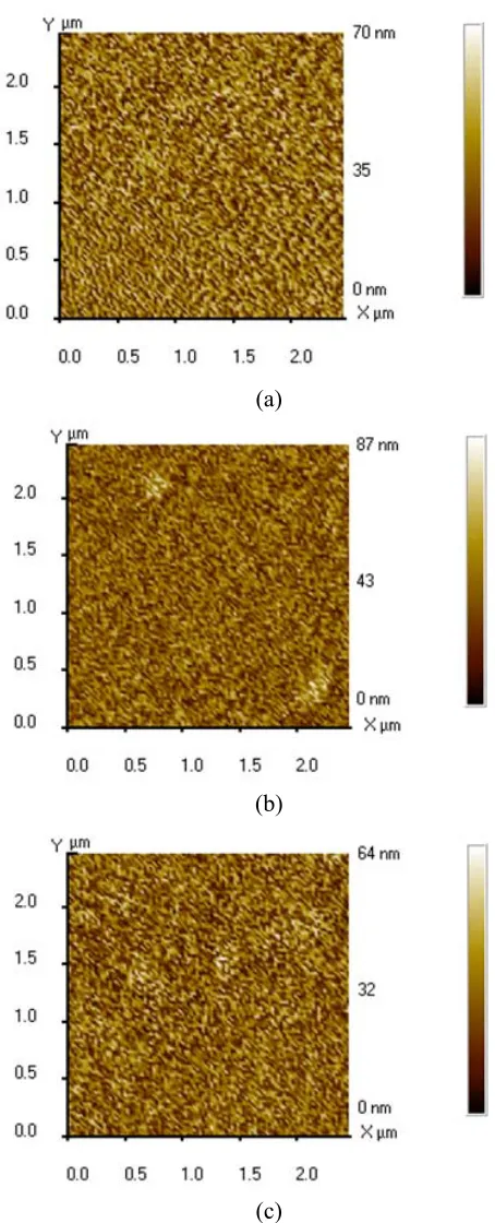
chips with different gold/silver thickness are reported in figure 1. It is observed that the chip's surfaces is relatively flat and smooth (Ra ≈ 12 ± 1.5 nm) and there is no obvious difference between them.
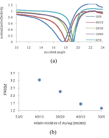
The SPR responses for the different configurations are plotted in figure 2-a [6]. As can be seen from this figure, different Gold/Silver thickness yield different SPR angles and curve width (FWHM). It can be observed that the single silver film resulted in the sharpest SPR response followed by various bi-layer metal films and finally the single gold layer film.
By using the double-layer metal film the problem of poor precision of a single-layer gold film is reduced, as can be seen from the much narrower width of the absorption peak produced and the problem of stability and poor chemical properties of a single silver film are overcome [2].
The FWHM of the SPR curves obtained from figure 2(a) are summarized in figure 2-b, a. The optimum Gold/Silver thickness is seemed to be the thickness which results in the minimum FWHM. For the double-layer design, various FWHM can be achieved with various silver–gold thicknesses. As observed from Figure 2(b), a thicker gold-thinner silver coating results in a SPR curve with broader FWHM, hence, lower sensitivity. Conclusively, by the Silver/glass layer composite achieves a FWHM is three times narrower than what can be achieved with the single gold film design. As such, a 62% FWHM and thus higher sensitivity can be achieved with the double-layer 20/30 arrangement as compared to the single gold film SPR sensor.
(a)
(b)
(c)
312 M. Ghorbanpour et al./ JNS 3 (2013) 309-313
(a)
(b)
Fig. 2. SPR curves (a) and related FWHM (b) of
different Gold/Silver bi-layer chips
The layer stability characteristics of the Gold/Silver /glass composite layers as a function of Gold/Silver thickness is summarized in table 1. It is observed that the Gold/glass composite layer does not pass the tape stability test. Only after the introduction of a 20 nm silver intermediate layer to the Gold/glass composite, it passes this test successfully. In other words, the mere introduction of Silver as an intermediate layer enhances the adherence of Gold to the glass substrate [6, 7].
Referring to table 1, it is observed that the SPR response of the Gold/Silver/glass composite layers after chemical stability test follow a different trend compared to the tape test. For the Gold/Silver composite layers, the 50/0 and 40/10 samples pass this test and show no changing in the SPR response as gold protective layer covers completely the chip surface.
Table 1. Stability tests of Gold/Silver /glass composite layers with different Gold/Silver thicknesses
Au/Ag
Tape Chemical test stability test
50/0 Passed
40/10 Passed
20/30 Passed 37.91% of SPR depth decreased
10/40 After 12 min detached
5/45 After 8 min detached
0/50 After 5 min detached
After the chemical stability test, it is observed that increment of silver thickness of the bimetallic composite layer weaken the SPR response of the chip. This is while the SPR signal of the 20/30 is still of a reasonable intensity ca. 37.91% reduction with respect to parent signal. Remain composite layers don’t pass chemical stability test. According to the stability results only the Gold/Silver sample with 20/30 thickness passed both tape test and chemical stability test.
4. Conclusion
313 M. Ghorbanpour et al./ JNS 3 (2013) 309-313
Moreover, the Silver layer (instead of usual Cr or Ti layer) was used as an adhesive intermediate layer between the Gold layer and the glass substrate. Further optimization of the Gold/Silver thickness using SPR analysis and stability tests showed that the 20/30 gold/silver bi-layer chip results in a better resolution, higher precision and more stable SPR sensing chip.
References
[1] B.H. Ong, X. Yuan, S.H. Tjin, J. Zhang, H.M. Ng, Sensors and Actuators B. 114 (2006) 1028– 1034.
[2] S. Zhang, L. Berguiga, J. Elezgaray, T. Roland, C. Faivre-Moskalenko, F. Argoul, Surf. Sci. 601 (2007) 5445–5458.
[3] A. Zynio Stepan, V. Samoylov Anton, R. Surovtseva Elena M. Mirsky, Vladimir, M. Shirshov Yuri, Sensors. 2 (2002) 62-70.
[4] X.C. Yuan, B. Hong, Y.G. Tan, D.W. Zhang, R. Irawan, S.C. Tjin, J. Opt. A Pure Appl. Opt. 8 (2006) 959–963.
[5] Y. Chen, R.S. Zheng, D.G. Zhang, Y.H. Lu, P. Wang, H. Ming, Z.F. Luo, Q. Kan, App. Optics. 50 (2011) 387-391.
[6] M. Ghorbanpour, C. Falamaki, App. Optics. 51 (2012) 7733-7738.