AES IMPLEMENTATIONS
AGAINST SIDE CHANNEL
ATTACKS
BASED ON POWER ANALYSIS
By:
Maarten Thoonen
EEMCS
Computer Architecture for Embedded Systems group
Bachelor Thesis
1 Thesis description
Contents
1 Thesis description 1
2 Introduction 3
3 Background 4
3.1 The Field-Programmable Gate Array . . . 4
3.2 The FPGA design flow . . . 9
3.3 RapidSmith2 . . . 12
3.4 The Advanced Encryption Standard . . . 13
3.5 Differential Power Analysis . . . 17
4 Method 20 4.1 Randomly Splitting LUTs . . . 20
4.2 Targeted LUT splitting . . . 21
4.3 Using Flip-Flops as logic elements . . . 21
5 Implementation 23 5.1 The AES Implementation . . . 23
5.2 Splitting LUTs . . . 24
5.3 Using Flip-Flops as gates . . . 24
6 Results 26 6.1 Device . . . 26
6.2 Measurement setup . . . 26
6.3 Measurement results . . . 27
7 Discussion 30 7.1 Results. . . 30
7.2 RapidSmith2 . . . 30
8 Conclusions 31
9 Recommendations 32
2 Introduction
In this work, new ways to protect an AES implementation from Differential Power Analysis-based Side Channel Attacks are researched. The project is partially a contin-uation on the master thesis of Gerhard Mlady [8]. That work explored among other things whether physically moving parts of an AES implementation to different parts of a device increased the DPA (Differential Power Analysis) resistance. As that was not the case, this work tries to find out whether other changes to the netlist will make a difference.
In a modern world with many privacy-sensitive data being send around the internet, data encryption is essential. A widely used encryption algorithm is AES (Advanced Encryption Standard). This algorithm has applications ranging from bank card security to hard disk encryption [14]. DPA (Differential Power Analysis) resilience is a topic of interest as in theory AES is a secure algorithm, but physical implementations make it vulnurable to attackers. It is therefore important to find out how to securely but efficiently implement the encryption algorithm on hardware like FPGAs. FPGAs are getting more and more popular as technology progresses. This is because on the one hand, bringing a custom ASIC to market is getting progressively costlier as production processes get more expensive the smaller the feature size becomes, making low volume chips uneconomic. On the other hand, those improved processes make ever more com-plicated FPGAs possible, enabling more complex and faster circuits to be implemented. Combining this with the fact that modern FPGAs, in particular MPSoCs that com-bine an FPGA with an SoC, open up opportunities previously not possible. That makes them very attractive options for a lot of projects and thus also cryptography applications. Examples of these opportunities include the option to update and patch hardware by reprogramming FPGAs, or even reprogramming them continuously. This last technique, called dynamic (partial) reconfiguration, enables techniques like storing many different circuits in the SoC part of an MPSoC and only implementing the circuit needed at the time, decreasing FPGA resource usage and static device power consumption. Another possible application is storing many variants of the same netlist. If a different circuit is used every time the AES algorithm is run, the power profile will be slightly different every run, which makes DPA harder.
3 Background
In this section, theoretical background knowledge is introduced. FPGA architecture and design flow are explained, along with a detailed explanation of AES and DPA.
3.1 The Field-Programmable Gate Array
To start, the general concept of a FPGA (Field-Programmable Gate Array) will be explained. An FPGA is a programmable piece of hardware, which makes it functionally inbetween ASIC and software. An ASIC (Application-Specific Integrated Circuit) is a very specialized chip designed to do one thing, whereas software can be written to do basically anything on a general purpose processor. An FPGA contains thousands (in some cases even millions) of small hardware elements that can be programmed and connected together to do certain tasks. Because of this, an FPGA has qualities of both software and hardware. It is flexible and can be programmed to do basically anything like software, but it also has the speed and energy efficiency advantages of hardware. Of course it is not as flexible as true software and not as efficient has true hardware, but it is a nice halfway point. The detailed explanation of an FPGA written below this will mostly target the Xilinx 7 Series architecture. This because the targeted device for this work is the AVNet Zedboard, containing a 7 Series FPGA.
3.1.1 Configurable Logic Block
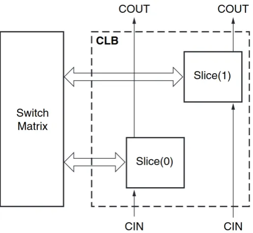
The main building block of an FPGA is a CLB (Configurable Logic Block). This CLB is in turn divided in two Slices, which contain a number of BELs (Basic ELements). In Xilinx Series 7 FPGAs, there are two kinds of Slices in CLBs: SLICELs and SLICEMs [20]. In Figure1 it can be seen how those Slices are situated within a CLB.
Figure 1: Location of the Slices within a CLB, along with the carry chain connections and the connection to the switch matrix. Taken from [20].
subtraction within a Slice. The Carry Chain has inputs from the LUTs or the Slice (bypassing the LUTs) and outputs to Flip-Flops and MUXes. An overview can be seen in Figure2. There are also connections to the Carry Chains of other Slices to form even longer carry chains by cascading them. They also feature lookahead logic for improved performance.
SLICEM A SLICEM contains the same elements as the SLICEL, with the addition of hardware to create 256 bits of Distributed RAM or 128 bits of Shift Register from the LUTs. The LUTs of a SLICEM can be configured to the following types of RAM:
- Single-port 32x1-bit using one LUT
- Dual-port 32x1-bit using two LUTs
- Quad-port 32x2-bit using four LUTs
- Simple dual-port 32x6-bit using four LUTs
- Single-port 64x1-bit using one LUT
- Dual-port 64x1-bit using two LUTs
- Quad-port 64x1-bit using four LUTs
Figure 2: Schematic overview of the Carry Chain within a Slice. Taken from [20].
- Single-port 128x1-bit using two LUTs
- Dual-port 128x1-bit using four LUTs
- Single-port 256x1-bit using four LUTs
The SLICEM shift register hardware enables every LUT to be used as a 32-bit shift register. The LUTs can be cascaded to form a shift register of up to 128 bits. Lengths are not limited to multiples of 32 bits, as the first five input pins of the LUT can be used as address pins to address every bit. That way any bit within the shift register can be chosen as the output bit. Synchronous reads can be implemented by utilizing the Flip-Flops in the Slice.
3.1.2 BRAMs
Some types of hardware are expensive to implement with just CLBs. An example of such a type of hardware is memory, both RAM and ROM. Therefore, the FPGA contains a number of BRAMs (Block RAMs). These are blocks of general purpose memory. In Xilinx Series 7 FPGAs, BRAM comes in blocks of 36Kb, which can also be configured as two independent blocks of 18Kb [21]. They can be configured from 32K of bit-addressable memory up to 512 blocks of 72-bit words, when using simple dual-port mode. In simple dual-part mode, each RAM block has one read port and one write port with independent clocks. Additionally, two BRAM blocks can be combined without any additional hardware into one bit-addressable 64Kb RAM block. All BRAMs support ECC memory protection. In addition to addressable RAM, the blocks can also be used as FIFO memory.
3.1.3 DSP blocks
Another type of hardware that is expensive to implement using CLBs is digital signal processing hardware. Because of that, the FPGA contains a number of DSP (Digital Signal Processing) Slices. 7-Series FPGAs contain DSP48E1 Slices which contain mul-tiply, multiply accumulate, multiply add, full adder, barrel shift, wide-bus multiplexing, magnitude comparator, bitwise logic, pattern detect and wide counter functions [22]. These elements enable applications such as FFT (Fast Fourier Transform) and floating point math. A number of registers are also included for pipelining, to increase clock speed at the expense of latency. The multiplier has two inputs, one for an 18-bit two’s complement operand and one for a 25-bit two’s complement operand. This produces a 43-bit result which is sign extended to 48 bits and then fed into the adder. When the multiplier is used, this is a two input 48-bit two’s complement adder. If the multi-plier is not used the adder can be used as a three-input 48-bit two’s complement adder. The adder can also be used as part of aSIMD(Single Instruction Multiple Data)ALU
(Arithmetic Logic Unit), supporting dual 24-bit or quad 12-bit operations. The opera-tions supported are adding, subtracting and an accumulator and every operand has a separate carry out signal.
when a predetermined pattern or the complement thereof is matched. Pins for Overflow and Underflow detection are also present.
DSP48E1 Slices have 18 control bits to control which input registers to use, which functions of the DSP Slice to use, cascading Slices and controlling the output. A detailed explanation of the control logic is outside of the scope of this description.
3.1.4 Routing and Clocking resources
The main routing resources are wire segments connected by switch matrices. These switch matrices consist of Programmable Interconnect Points orPIPs. Lines of different lengths ensure that every part of the FPGA is reachable for the CLBs. Longer lines allow quick connections to far-away parts of the FPGA while short lines allow for every part to be reachable.
3.1.5 ZYNQ Processing System
The FPGA in the Zedboard is not only an FPGA, but also contains anSoC (System on Chip). Therefore, Xilinx calls it anMPSoC. MPSoC means Multi-Processor System on Chip. ZYNQ MPSoCs contain a Series 7 FPGA (the Programmable Logic orPL) and a dual-core Cortex A9 ARM SoC (the Processing System orPS) [25]. Between those two parts are strong connections, so they can work closely together. The processing system always boots first, allowing partial dynamic reconfiguration. This means that the logic part of the ZYNQ can be (partially) reprogrammed while the processing system keeps running. The PS has many types of I/O, including, but not limited to GPIO pins, two gigabit ethernet controllers, two multifunctional usb controllers (host, device and OTG), SD card support, two SPI controllers, two UART controllers and two I2C controllers. The Processing System and Programmable Logic are connected with an interconnect called AXI (Advanced eXtensible Interface). This provides connectivity between the system memory, CPU, Programmable Logic and the various interface controllers. Using this bus, IP (more about this later in chapter3.2.2) implemented in the PL can talk to the CPU and vice versa.
3.1.6 FPGA power consumption
The power consumption of an FPGA is build up from different parts. The main parts are the Device Static Power and the Design (or Dynamic) Power [19]. The Device Static Power includes the Quiescent Current of the device. The Design Power is the important part (at least for this work) of the power consumption. It includes the power consumed by all design elements of the implementation loaded on the device. A notable exception is the Off-Chip Power, which is the current the I/O pins deliver to outside board components. This is not included in the Design Power, as the Design Power and Device Static Power together form the Total On-Chip Power, which is important to calculate the thermal dissipation requirements for the FPGA.
3.2 The FPGA design flow
TCL console. TCLis an interpreted programming language that can be used to generate scripts for Vivado.
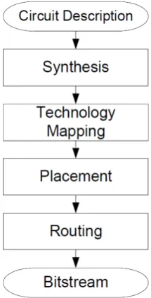
Figure 3: Block diagram of the FPGA design flow. The ’Synthesis’ from this diagram is called ’RTL analysis’ in Vivado and ’Technology Mapping’ is called ’Synthesis’ in Vivado. Adapted from [16].
3.2.1 HDL code
There are two main programming languages for programming hardware and thus FP-GAs. These are VHDL and Verilog. The base design from Gerhard Mlady [8] is in VHDL and it is also the only language I have used before. Therefore, this language will be used for this project.
VHDL stands for VHSIC Hardware Description Language. VHSIC, in turn, stands for Very High Speed Integrated Circuit. This already gives a good idea of what the language is: a language to describe complicated integrated circuits. VHDL code consists of two parts: the architecture of the design and the behaviour of said architecture. The architecture lists all the entities and their ports in a design, while the behaviour describes what all the parts do exactly. VHDL can be used to describe all kinds of hardware, so not just FPGAs. ASICs can also be designed with VHDL.
should be placed, but also information about which ports should be bound to certain physical pins of the FPGA or clock information.
Another possibilty for programming FPGAs is HLS (High-Level Synthesis). With HLS, ’normal’ programming languages like C, C++ or Haskell are used to program the functionality of a design. Instead of compiling it to machine code, it is compiled to hardware.
3.2.2 IP block design
Vivado contains a large number of so-calledIP (Intellectual Property) Cores. An exam-ple of this is the ZYNQ processor system, which can be added as an element in a block design. Other examples are the MicroBlaze system, a CPU made up of logic elements, and interface controllers like PCI Express, Ethernet and audio/video hardware.
User generated IP can also be added. Vivado projects can be created ’out of context’, so without any outside connections. Those projects can then be packaged as IP cores which can be reused in other designs as building blocks. By creating a block design, all the IP cores can be connected to each other and to outside ports. Vivado can automatically generate wrapper VHDL code for synthesis and simulation. Cores can be connected by simple wire connections, using protocols like UART or a more advanced protocol like AXI.
3.2.3 RTL netlist analysis and simulation
Vivado creates an RTL (Register Transfer Level) netlist from the HDL code, a netlist with registers and logic gates. This netlist contains mainly RAM, registers and MUXes and can be used to simulate the design. Both the behaviour and the timing of the design can be evaluated by writing a test bench in an HDL. These test benches can be used to apply stimuli to the inputs of the design without having to physically implement the desing on an FPGA.
3.2.4 Synthesis
no BRAMs or DSP slices in designs. RapidSmith2 is more tuned towards the Vivado design flow and thus supports more elements. More about RapidSmith2 can be read in chapter 3.3.
3.2.5 Implementation
After synthesis, the primitives need to be mapped to suitable BELs of the FPGA. Also, the design has to be routed, meaning connection paths need to be found between all design elements. Vivado does this automatically in the Implementation step. In tcl, this step is split into two steps: place_design androute_design.
3.2.6 Writing the design to the FPGA
Finally, the implementation needs to be written to the FPGA. Vivado does this by generating a bitstream from the implementation. This is all proprietary, so this bitstream can not be edited (much) after it is generated.
3.3 RapidSmith2
RapidSmith2is a package of Java classes with functions to put RapidSmith Checkpoints into objects, which can then be manipulated. RapidSmith2 can manipulate designs on the BEL level for placement and PIP level for routing. It is developed by the CHREC group of the Brigham Young University in the US [9]. It is a continuation of the Rapid-Smith project which was written for ISE, the predecessor of Vivado. RapidRapid-Smith was also developed by the BYU. It was adapted to Vivado by using Tincr [17] to generate RapidSmith checkpoints from designs. Recently, another fork of RapidSmith was devel-oped called RapidWright [26]. This program also consists of a package of Java classes, but stores designs a bit differently. It is also considerably newer and only works properly with Vivado 2018.3 and up. RapidWright is developed by Xilinx Research Labs.
Designs can be imported into RapidSmith2 from RapidSmith checkpoints. Rapid-Smith checkpoints can be created at different points in the design flow, as illustrated in Figure4. The checkpoints are generated byTincr, which is an API that uses Vivado’s in-terpreted programming language tcl to generate files that can be read by RapidSmith2. When a checkpoint is imported into RapidSmith2, it is split into three objects: the design, device and the cell library.
Design In the design, the actual netlist and supporting information is stored. This contains all the elements from the project and their locations. In this object, all the BELs, the map of how they are connected and the supply nets VCCnet and GNDnet are stored.
about the device family.
[image:14.595.95.506.179.338.2]Cell library In the Cell library object, all the different cell types that are supported by the device are stored as LibraryCells. They contain information about the characteristics of all the BELs.
Figure 4: Overview diagram of the different points in the design flow checkpoints can be im- or exported. Taken from [9].
Most information is stored in the Design object. The Design consists of two main types of objects: Cells and CellNets. Cells represent the BELs in the design while CellNets are the connections between them. Every basic object of the design can be explored and changed. From a BEL its pins and the CellNets connected to those pins can be found. Entirely new elements can be added as well, which can then be connected to existing pins. The design can also be routed by hand by traversing through all the switchboxes in the device, if highly custom routing is necessary.
3.4 The Advanced Encryption Standard
The Advanced Encryption Standard, AES for short, is the standard encryption algorithm used by the federal government of the US [10]. It is based on the Rijndael algorithm. It is ablock cipher, which means it encrypts data in block of a certain size. AES encrypts data in blocks of 128 bits and can use keys of length 128, 192 and 256 bits. The algorithm consists of two parts: the cipher and the key expansion algorithm.
3.4.1 Cipher
The cipher consists of four main operations: SubBytes(),ShiftRows(),MixColumns()
Figure 5: Graphical representation of the ShiftRows() operation. Image taken from [10]
MixColumns() and AddRoundKey() are executed after eachother 10 times for a 128-bit key, 12 times for a 192-bit key and 14 times for a 256-bit key. The final round is slightly different: theMixColumns() operation is ommitted.
SubBytes() The SubBytes() operation works on every byte independently. It is a non-linear byte substitution using a substitution table called the S-box. This S-box is invertible, so the operation can be reversed when decoding.
ShiftRows() During the ShiftRows operation all the rows of the state are shifted 0, 1, 2 or 3 bytes to the left, from top to bottom. Values that ’fall off’ at the left side are moved to the right side of the row. An illustration can be seen in Figure 5
MixColumns() In the MixColumns() operation, the columns of the state are multi-plied by the following polynomial:
a(x) ={03}x3+{01}x2+{01}x+{02} (1)
Where the numbers in curly brackets are hexadecimal.
This can best be illustrated by writing it in matrix form:
S0′,c S1′,c S2′,c S3′,c
=
02 03 01 01 01 02 03 01 01 01 02 03 03 01 01 02
S0,c
S1,c
S2,c
S3,c
AddRoundKey() The last operation is the addition of the round key. The round key is generated during the key expansion phase and is simply XORed with the state.
3.4.2 Key Expansion
The Key Expansion algorithm generates a total of 4×(number of rounds + 1) 4-byte words from the initial key. The Key Expansion algorithm has two functions: SubWord()
and RotWord(). It also uses a special array Rcon[]. The algorithm is hard to explain in text, so it is explained with the help of some pseudo code, taken from [10]:
1 KeyExpansion (byte key [4* Nk], word w[Nb *( Nr +1)], Nk) 2 begin
3 word temp
4
5 i = 0 6
7 while (i < Nk)
8 w[i] = word(key [4*i], key [4*i+1] , key [4*i+2] , key [4*i+3])
9 i = i+1
10 end while 11
12 i = Nk 13
14 while (i < Nb * (Nr +1)] 15 temp = w[i -1]
16 if (i mod Nk = 0)
17 temp = SubWord ( RotWord (temp)) xor Rcon[i/Nk] 18 else if (Nk > 6 and i mod Nk = 4)
19 temp = SubWord (temp)
20 end if
21 w[i] = w[i-Nk] xor temp 22 i = i + 1
23 end while 24 end
is divisible by the number of columns of the key, the temp variable is run through the
RotWord() function, XORed by the Rcon[] value for the word and the result is run through SubWord(). Only then is it XORed withw[i-Nk]. There is an extra rule if the number of columns in the key is larger than 6, so if a 256-bit key is used. Then, every 4th word is also run through SubWord().
SubWord() This function applies the S-box substitution table to each of the bytes of a 4-word input word.
RotWord() RotWord() also takes a 4-byte input word an shifts the bytes one byte to the left, and the former first byte is moved to the end.
Rcon[] Rcon[], the round constant word arrays, contains values given by:
[{02}i−1,{00},{00},{00}] (3)
Again, numbers in curly brackets represent hexadecimal numbers.
3.4.3 Reverse Cipher
An encryption algorithm would be no good if there was no way to decrypt the cipher-text. The decryption algorithm for AES is similar to the encryption algorithm. The
AddRoundKey()function is the same, the other functions are changed toInvShiftRows(),
InvSubBytes() and InvMixColumns(). InvShiftRows() is the same as ShiftRows()
but the rows are shifted to the right instead of the left. InvSubBytes()uses the inverted version of the S-box. TheInvMixColumns() function uses the following polynomial:
a−1(x) ={0b}x3+{0d}x2+{09}x+{0e} (4)
Resulting in the following matrix:
S0′,c S1′,c S2′,c S3′,c
=
0e 0b 0d 09 09 0e 0b 0d
0d 09 0e 0b
0b 0d 09 0e
S0,c
S1,c
S2,c
S3,c
for0≤c <3 (5)
3.4.4 Security
AES, but had not found any by 2012 [14]. This all means that breaking the cipher itself is not possible at this point in time. Therefore, other methods like side channel attacks need to be used to uncover information encrypted with AES. Side channel at-tacks target a specific implementation of a cryptographic algorithm. For software this could be measuring how long computations take, but for this research physical attacks on hardware are more relevant. Physical attacks need access to the device the algorithm is running on, they can not be conducted on raw ciphertext (encrypted data), plaintext
(unecrypted data) or key data. Research [15] hows that it is possible to break a block cipher implementation on an FPGA by employing a side channel attack called Differ-ential Power Analysis. Another paper [5] even shows that it is possible to break AES encryption using this technique in only a matter of hours. Note that the last attack was on flash-based FPGAs, which typically have lower power consumption and better power characteristics than SRAM-based FPGAs, which the Xilinx 7 Series FPGAs are. Break-ing into SRAM-based FPGA AES implementations is even easier. The next chapter will give a more detailed explanation of DPA and possible countermeasures.
3.5 Differential Power Analysis
3.5.1 Existing countermeasures
The easiest way to prevent DPA side channel attacks is of course to prevent physical access to the circuit. However, this is not always possible or feasible. Below a few existing countermeasures are outlined.
Random order execution The AES algorithm has two characteristics that makes it possible to make it DPA-resistant: the order of the operations can be changed and the operations can be done to every byte of a 128-bit block individually. By shifting the order of the operations for every byte of a block, DPA resistance is greatly increased [1]. This technique works well, but needs a true random number generator (TRNG) to be completely secure. Low-cost ultra-low-power hardware currently often does not have such a TRNG. The algorithm is also of course completely different from the standard algorithm.
Voltage regulator based resistance Many chips have voltage regulation circuitry on board. With a simple voltage regulation circuit, the input current is proportional to the output current of the regulator and thus DPA can be conducted on the input current of the voltage regulator. However, if the voltage regulator is constructed in such a way that the input current is less proportional to the output current, DPA resistance is greatly increased [27]. Of course, changing the actual power delivery circuitry of a design is often not possible or impractical, making this only useful for highly custom designs.
Masking One of the earliest countermeasures was masking. With masking, sensitive data is split into so-called shares. All shares are statistically independent and thus a subset of shares contains no information about the data. The cryptographical opera-tions are then done for all shares, so the partial key cannot be determined from one measurement. The different steps in the process have to be adapted to the masked data to function correctly [3]. A disadvantage of masking is that it has a large area or memory overhead and requires a TRNG [11].
Ring oscillators Another countermeasure is making use of ring oscillators in the circuit. By implementing twelve ring oscillators close to the S-box and making them randomly activate based on S-box inputs essentially drowns out the leaking information from the S-box. The random activation is achieved by XORing the input bytes with a random value. Twelve oscillators are needed, because a minimal of two oscillators need to be active simultaneously to drown out the signal from the S-box, at least for 90nm silicon [12]. Disadvantages of this technique are that it is highly technology dependent and increased power consumption of the implementation.
value before the actual value is send over them. Because of that, the signal send over the one wire is the exact opposite of the other wire. This ensures that the power signature is independent of and equal for all data being send over the wires and thus makes power analysis attacks impossible [13]. Although this works perfectly in theory, in practice it is hard to match the two wires exactly, causing small leakages of data. Also, implementing this in FPGAs effectively doubles the amount of connections, increasing power usage and possibly creating routing bottlenecks.
4 Method
To decrease the feasibility of Differential Power Analysis Side Channel Attacks, the power consumption needs to be less predictable or harder to measure. The techniques discussed in 3.5.1 are either not implementable with an FPGA, need an TRNG, need a custom implementation of the AES algorithm or have significant overhead. This work looks into modifications of the netlist of an existing AES implementation to find out whether it can be made DPA resilient. The netlist needs to be modified in such a way that the power consumption is less dependent on the data the circuit is processing. Below, a number of techniques to do this are outlined.
4.1 Randomly Splitting LUTs
[image:21.595.192.405.319.503.2]Larger lookup tables of length n can be made by combining two lookup tables of length n-1 and a MUX, as seen in Figure6. Incidentally, this is also the way LUT6 primitives are constructed in silicon from two LUT5 circuits and a MUX in Series 7 FPGAs.
Figure 6: Schematic image of how a LUT6 can be constructed from two LUT5s and a MUX. Taken from [4].
Figure 7: The two primitives that can be made from a Flip-Flop. Taken from [20]
Figure 8: The way the Flip-Flop needs to be wired for an OR2L primitive. Taken from [20]
automatically place and route the new cells. By randomly selecting Cells to be changed, the changes in power consumption are unpredictable. Certain keys might activate more LUTs than other keys, which either makes DPA more difficult as the power consumption less correlated to the data or it might make it easier, if the power usage depends more on the key being used. Still, this is used as a starting point.
4.2 Targeted LUT splitting
Some parts of the design have more impact on the power profile than other parts. For ex-ample, the serial communications part of the design has no impact on the cryptographic information in the power profile. When conducting a DPA attack on an AES implemen-tation, the partial key can be found by measuring the power usage of theAddRoundKey()
or theSubBytes()stage of the algorithm [8,15]. Therefore, if one or both of these parts of the circuit are targeted, more gains could be made in power profile obfuscation with a smaller increase in total area and power consumption than is the case for random splitting.
4.3 Using Flip-Flops as logic elements
5 Implementation
The targeted device is the AVNet Zedboard, a prototype board with a Xilinx XC7Z020-CLG484-1 AP SoC. This is a chip with two ARM cores and an FPGA with 85k logic cells. Other features of the FPGA include 4.9Mb of Block RAM, 220 DSP slices and a maximum of 200 I/O pins. This device is used as it is the same device used in [8] and because is readily available for this work. RapidSmith2 will be used to implement the algorithms, as it better supports the design elements of a Xilinx FPGA and it is easier to import and export checkpoints from and to Vivado than it is with ABC. RapidWright was considered, but in the end not used as access to Vivado 2018.3 came relatively late during the project and at that point more knowledge about RapidSmith2 was gathered.
5.1 The AES Implementation
The AES implementation used will be the same as from [8]. This is a 128-bit AES implementation consisting of an encoder, decoder, key expansion module and RS232 serial interface. It can be adapted to 192 and 256 bits, but not on the fly. For the proof of concept just the 128-bit version is used. The RS232 interface uses the UART
protocol, which dictates that the input is high by default. Every byte has a preceding 0 as a start bit and a 1 as a stop bit. A graphical representation can be found in Figure9.
[image:24.595.100.494.389.413.2]start bit bit 0 bit 1 bit 2 bit 3 bit 4 bit 5 bit 6 bit 7 stop bit
Figure 9: Schematic representation of UART signalling a single byte of information. Image taken from [18].
A number of control bytes are used to control the circuit. These are the following (all representations in hexadecimal):
- 4bto set the device to key input mode
- 41to set the device to data input mode
- 52to tell the device the ciphertext or plaintext should be send back over UART
- 53to tell the device a reply is not needed
- 45to set the device to encrypt mode
- 44to set the device to decrypt mode
- 43to start the de/encryption process
So a typical dataflow to let the device encrypt a single datablock and get the ciphertext back is the following: 4b -> 16 bytes of key data -> 41 -> 16 bytes of plaintext -> 52
5.2 Splitting LUTs
A Java program is written to find and split LUT6s using RapidSmith2. First, it gets all LUT6 primitives and puts them in an ArrayList of Cells. In the simplest version of the algorithm, it traverses through this array and randomly adds LUTs to the queue to be split. For every LUT6 to be split the program adds two LUT5 primitives to the design, along with a MUXF7 primitive. Then, input pins 0 to 4 of the LUT6 are connected to the input pins of both of the LUT5s. The outputs of the LUT5s are connected to the MUXF7 inputs while input pin 5 of the LUT6 is connected to the input selection port of the MUXF7. When that is done, the output of the MUXF7 is connected to the port the output of the LUT6 was connected to. All of the CellNets are disconnected from the LUT6. The INIT string attribute of the LUT6 is split and both halves are written to the correct LUT5 primitive. Finally, the old LUT6 primitive is deleted. A TCP is created to be imported into Vivado, which will take care of placement and routing.
5.2.1 Targeted Splitting
All elements in the netlist have a human-identifiable name. Therefore, if the algorithm searches the list of BELs and selects only the elements with subbytes and roundkey in the name, the SubBytes() and AddRoundKey() operations are targeted. This is the only change to the simple LUT splitting algorithm; instead of randomly selecting LUT6s, LUT6s with those words in the name are selected. This can be implemented with a simple If statement, with the condition that those words are in the ’name’ string of the BEL.
[image:25.595.201.386.461.570.2]5.3 Using Flip-Flops as gates
Figure 10: Schematic representation of the LUT2 primitive. Taken from [24].
O column, with INIT[0] being the LSB. Prepended is the string 4'h. This makes the INIT string for the AND2B1L primitive 4'h2 and for the OR2L primitive 4'hE. The algorithm can then search for all LUT2 primitves, compare their INIT string attributes with those two strings and select the LUT2s with the correct INIT strings. The correct Flip-Flop primitive can then be added to the design. The inputs and outputs of the LUT2 primitive then have to be connected to the new AND2B1L or OR2L primitive and lastly the old primitive is deleted.
Table 1: Truth table for the LUT2 primitive I1 I0 O
0 0 INIT[0] 0 1 INIT[1] 1 0 INIT[2] 1 1 INIT[3]
Table 2: Truth table for the AND2B1L primitive I1 I0 O
0 0 0 0 1 1 1 0 0 1 1 0
Table 3: Truth table for the OR2L primitive I1 I0 O
6 Results
In the following section will be outlined how the algorithms are validated. The algorithms are simulated in different ways outlined in Section6.2.1. Results from these simulations and the observations made from those results are in Section6.3.
6.1 Device
To obtain measurement results, in the end the XC7A100-TCSG-324-1 (Series 7 Artix) device was used. There were some issues with incompatibility between the ZYNQ device and the 2.0.0 version of RapidSmith2, which was desirable to use because of other bug fixes. A fix for the ZYNQ part is in the works, but was not yet available when results had to be obtained. The Artix device FPGA is a bit larger than the FPGA portion of the ZYNQ device, with 101440 logic cells instead of 85000. Another difference is of course that the Artix does not have the SoC part the ZYNQ has. Though as the FPGA architecture is exactly the same and the SoC part is not used, this device should be identical in terms of functionality for this design. The Artix is the ’default’ device in RapidSmith2, in the sense that it is the example device in the documentation [9]. It is therefore well-supported and relatively bug free.
6.2 Measurement setup
6.2.1 Measured designs
A total of fourteen simulations are run:
- One is the control simulation, run with a netlist generated directly from the VHDL code and not run through RapidSmith2
- One is a control simulation with the netlist from the first simulation imported and exported into RapidSmith2, but otherwise not changed in any way
- Three are run with just the LUT6 splitting algorithm, with 10%, 50% and 100% of all LUT6s split
- Three are run with the targeted LUT6 algorithm, with 10%, 50% and 100% of all LUT6s of theaddRoundKey()and SubBytes()operations split
- Three are run with just the LUT2 to Latch algorithm, with 10%, 50% and 100% of eligible LUT2s transformed
- The last three are run with a combination of the random LUT6 splitting and LUT2 transforming algorithms, with both algorithms running at 10%, 50% and 100%
The LUT2 algorithm is only run with random LUT2s, as there are not that much suitable LUT2s to begin with.
6.3 Measurement results
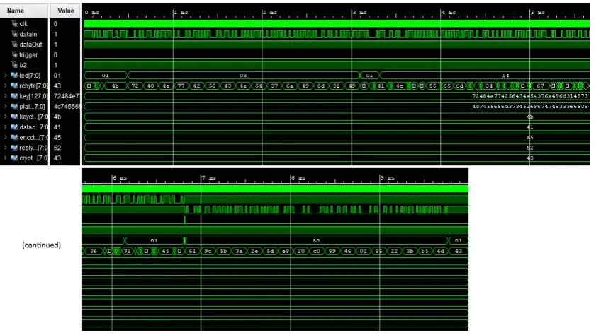
A typical measurement result looks like the scope screenshot in figure11. The ciphertext output can be read by reading the bytes from the rcbyte signal during the ’sending’ phase, indicated by the led vector with value 80. The first byte is a control byte and should be ignored. So in this case it can be seen that the correct ciphertext is generated, with value9c 5b 3a 2e 5d e8 20 c0 89 46 02 86 22 3b b5 4d. The results of all the simulations can be found in table4.
Every simulation takes about ten minutes, which includes running the algorithm Java program, importing the TCP into Vivado, compiling and running the simulation and then reading the results from the waveform and running the power estimation. By far the longest part of that is running the simulation. The amount of cells changed is not always exactly the same when using the same percentage, as it uses a random number generator to choose LUTs. The control design has 3985 Cells. The design with the most cells changed (both the LUT2 and LUT6 algorithms at 100%) has 6495 cells, or a 63% increase in cells used. As not all CLBs were full, this does not lead to a 63% increase in FPGA resource use, though.
Figure 11: Screenshot of the scope with simulation outputs for the control design. Part of the screenshot is cut of the end and pasted below in an effort to improve legibility.
Table 4: Simulation results
Algorithm Output Correct Cells changed Power usage Control 9c 5b 3a 2e 5d e8 20 c0 Yes 0 112 mW
89 46 02 86 22 3b b5 4d
Control 2 9c 5b 3a 2e 5d e8 20 c0 Yes 0 109 mW
89 46 02 86 22 3b b5 4d
LUT6 random 10% 9c 5b 3a 2e 5d e8 20 c0 Yes 124 LUT6s 109 mW
89 46 02 86 22 3b b5 4d
LUT6 random 50% 9c 5b 3a 2e 5d e8 20 c0 Yes 651 LUT6s 111 mW
89 46 02 86 22 3b b5 4d
LUT6 random 100% 9c 5b 3a 2e 5d e8 20 c0 Yes 1265 LUT6s 116 mW
89 46 02 86 22 3b b5 4d
LUT6 targeted 10% 9c 5b 3a 2e 5d e8 20 c0 Yes 37 LUT6s 109 mW
89 46 02 86 22 3b b5 4d
LUT6 targeted 50% 9c 5b 3a 2e 5d e8 20 c0 Yes 177 LUT6s 111 mW
89 46 02 86 22 3b b5 4d
LUT6 targeted 100% 9c 5b 3a 2e 5d e8 20 c0 Yes 343 LUT6s 113 mW
89 46 02 86 22 3b b5 4d
LUT2 random 10% 9c 5b 3a 2e 5d e8 20 c0 Yes 10 LUT2s 109 mW
89 46 02 86 22 3b b5 4d
LUT2 random 50% 9c 5b 3a 2e 5d e8 20 c0 Yes 36 LUT2s 109 mW
89 46 02 86 22 3b b5 4d
LUT2 random 100% 9c 5b 3a 2e 5d e8 20 c0 Yes 72 LUT2s 109 mW
89 46 02 86 22 3b b5 4d
LUT2 random 10% 9c 5b 3a 2e 5d e8 20 c0 Yes 10 LUT2s & 109 mW & LUT6 random 10% 89 46 02 86 22 3b b5 4d 117 LUT6s
LUT2 random 50% 9c 5b 3a 2e 5d e8 20 c0 Yes 38 LUT2s & 112 mW & LUT6 random 50% 89 46 02 86 22 3b b5 4d 653 LUT6s
7 Discussion
First the results of the work are discussed. After that, the choice for RapidSmith2 is discussed.
7.1 Results
As there turned out to be too little time to conduct measurements on a real FPGA, it was not possible to determine whether the algorithm works to improve DPA resistance. This was because of a larger workload than anticipated delayed a working algorithm and because there was no place where a measurement setup could be placed undisturbed. The necessity to learn how to use Vivado, how to program in Java, how the RapidSmith2 package works and how to write VHDL testbenches along with doing general research into FPGA architecture and DPA literature took a lot of time. This had the result that for me personally the project was very useful, as I learned a lot about those subjects. However, it also meant that I only have limited results in the end. I am happy with the fact I had two working algorithms in the end, of which I am fairly confident they can be used on physical FPGAs when RapidSmith2 is fixed so that the LUT RAMs can be placed by Vivado. The LUT2 to Flip-Flop algorithm might need an additional LUT as a routethrough from the switch matrix to the Latch as it shows this in the documentation as an example implementation. Though probably this is just for illustrative purposes as in theory there are direct connections from the Slice inputs to the Flip-Flops. Otherwise, it is relatively easy to add a LUT in RapidSmith2.
7.2 RapidSmith2
8 Conclusions
The main conclusion that can be drawn from this work is that RapidSmith2 can be used to change the netlist of an implementation at the BEL level while preserving function-ality. All algorithms produced correct results, at least in a post-synthesis simulation.
It also showed that a very large part of the design was made up of LUT6 primitives. When those are doubled into two LUT5s and an additional MUX is added, the total power consumption increases with 6.3%. A side note has to be made for this, though. Vivado estimates the power consumption by assuming all signals have a 12.5% switching rate. In reality, only small parts of the circuit are active at the time. For example, the encoding and decoding parts are never used simultaneously. It was not possible to estimate the power consumption while considering the switching activity, as generating a switching activity file is only supported RTL simulations from Verilog code with the Vivado simulator. As the source code was VHDL and the post-RapidSmith simulations are done with a synthesized edif (Electronic Design Interchange Format) netlist, this was not possible to do. Similarly, the 63% increase in Cells utilization does not necessarily lead to a 63% increase in FPGA resource utilization. Not all CLBs were fully utilized, so it is possible Cells can be placed in already-used CLBs. But again as implementation was not possible, the actual increase could not be determined.
9 Recommendations
The first recommendation is of course to test the algorithms on a physical FPGA and to perform side channel attacks on it, to find out if the implementation works on a real FPGA and to find out whether DPA resistance is increased. From this could be concluded what algorithm works best. It would be interesting to see if the targeted algorithm has the same effect as the random algorithm. Logically, you could conclude that not the entire implementation needs to be changed, for example the serial communication part has no influence on DPA resistance. To conduct the measurements, the RapidSmith2 patch needs to be released and a measurement setup needs to be build. Most of the test setup can reused from [8]. For this setup a place has to be found where little outside disturbance is present. The power supply pin is very small, so the probe needs to be placed very carefully. It might lose contact with the slightest movement, so therefore a quiet place is needed.
A second recommendation is a more involved algorithm. It would be nice if entire parts of the logic tree could be rewritten to a different structure instead of just single gates. When many different netlists can be generated very easily, partial reconfiguration can be used to continuously change the circuit. As this causes every measurement to be slightly different, side channel attacks become a lot harder.
References
[1] Bo, Y., Xiangyu, L., Cong, C., Yihe, S., Liji, W., Xiangmin, Z. (2012). An AES chip with DPA resistance using hardware-based random order execution. Journal of Semiconductors, 33(6). Retrieved fromhttp://iopscience.iop.org/article/ 10.1088/1674-4926/33/6/065009/meta
[2] Bogdanov, A., Khovratovich, D., & Rechberger, C. (2011).Biclique Cryptananalysis of the Full AESRetrieved fromhttps://web.archive.org/web/20120905154705/ http://research.microsoft.com/en-us/projects/cryptanalysis/aesbc.pdf
[3] Chari, S., Jutla, C. S., Rao, J. R., & Rohatgi, P. (1999). Towards Sound Approaches to Counteract Power-Analysis Attacks.Advances in Cryptology - CRYPTO’ 99, 398-412.https://doi.org/10.1007/3-540-48405-1_26
[4] Flex Logix. (2017). [LUT6 from two LUT5s and a MUX] [Illustration]. Retrieved fromhttp://www.flex-logix.com/6lut-faster-denser/
[5] Kamoun, N., Bossuet, L., Ghazel, A. (2009). Experimental implementation of DPA attacks on AES design with Flash-based FPGA technology.2009 6th International Multi-Conference on Systems, Signals and Devices. https://doi.org/10.1109/ ssd.2009.4956747
[6] Kocher, P., Jaffe, J., Jun, B. (1999). Differential Power Analysis.Advances in Cryp-tology - CRYPTO’ 99, 388-397.https://doi.org/10.1007/3-540-48405-1_25
[7] Mishchenko, A. (Last update 2012). ABC: A System for Sequential Synthesis and Verification. Retrieved fromhttps://people.eecs.berkeley.edu/~alanmi/abc/
[8] Mlady, G. (2018). Generierung und Evaluierung von Implementierungsvarianten zum Schutz von FPGA-basierten kryptographischen Implementierungen vor Seit-enkanalanalyse(MSc. thesis).
[9] Nelson, B., Townsend, T., & Haroldsen, T. (2018). RAPIDSMITH2 A Library for Low-level Manipulation of Vivado Designs at the Cell/BEL Level Technical Report and Documentation. Retrieved from https://github.com/byuccl/RapidSmith2/ blob/master/docs/TechReport/TechReport.pdf
[10] NIST. (2001).Announcing the / Specification for the ADVANCED ENCRYPTION STANDARD (AES).Retrieved fromhttp://nvlpubs.nist.gov/nistpubs/FIPS/ NIST.FIPS.197.pdf
[11] Petrvalsky, M., & Drutarovsky, M. (2016). Constant-weight coding based software implementation of DPA countermeasure in embedded microcontroller. Micropro-cessors and Microsystems, 47, 82-89.https://doi.org/10.1016/j.micpro.2016. 01.002
and Systems II: Express Briefs, 57(7), 546-550.https://doi.org/10.1109/tcsii. 2010.2048400
[13] Popp, T., Mangard, S., & Oswald, E. (2007). Power Analysis Attacks and Counter-measures IEEE Design & Test of Computers, 24(6), 535-543. https://doi.org/ 10.1109/mdt.2007.200
[14] SPIEGEL staff. (2014, December 28). Inside the NSA’s War on Internet Secu-rity. Spiegel. Retrieved from http://www.spiegel.de/international/germany/ inside-the-nsa-s-war-on-internet-security-a-1010361.html
[15] Standaert, F., Mace, F., Peeters, E., & Quisquater, J. (2006). Updates on the Security of FPGAs Against Power Analysis Attacks. Reconfigurable Computing: Architectures and Applications, 335-346.https://doi.org/10.1007/11802839_42
[16] Tom, M. (2002). CHANNEL WIDTH REDUCTION TECHNIQUES FOR SYSTEM-ON-CHIP CIRCUITS IN FIELD-PROGRAMMABLE GATE ARRAYS
[17] White, B., & Nelson, B. (2017).Tincr A Tcl-based CAD Tool Framework for Xilinx’s Vivado Design Suite. Retrieved from https://github.com/byuccl/tincr/blob/ master/README.md
[18] Wikipedia contributors. (2018, December 30). Universal asynchronous receiver-transmitter - Wikipedia. Retrieved from https://en.wikipedia.org/wiki/ Universal_asynchronous_receiver-transmitter
[19] Xilinx. (2013). Vivado Design Suite User Guid Power Analysis and Optimization. Retrieved fromhttps://www.xilinx.com/support/documentation/sw_manuals/ xilinx2012_4/ug907-vivado-power-analysis-optimization.pdf
[20] Xilinx. (2016). 7 Series FPGAs Configurable Logic Block User Guide. Re-trieved from https://www.xilinx.com/support/documentation/user_guides/ ug474_7Series_CLB.pdf
[21] Xilinx. (2016). 7 Series FPGAs Memory Resources User Guide. Re-trieved from https://www.xilinx.com/support/documentation/user_guides/ ug473_7Series_Memory_Resources.pdf
[22] Xilinx. (2018). 7 Series DSP48E1 Slide User Guide. Retrieved from
https://www.xilinx.com/support/documentation/user_guides/ug479_ 7Series_DSP48E1.pdf
[23] Xilinx. (2018). 7 Series FPGAs Clocking Resources User Guide. Re-trieved from https://www.xilinx.com/support/documentation/user_guides/ ug472_7Series_Clocking.pdf
[25] Xilinx. (2018). Zynq-7000 SoC Technical Reference Manual. Retrieved from https://www.xilinx.com/support/documentation/user_guides/ ug585-Zynq-7000-TRM.pdf
[26] Xilinx. (2019). RapidWright Documentation. Retrieved from http://www. rapidwright.io/docs/index.html
![Figure 2: Schematic overview of the Carry Chain within a Slice. Taken from [20].](https://thumb-us.123doks.com/thumbv2/123dok_us/9653232.467316/7.595.156.436.99.455/figure-schematic-overview-carry-chain-slice-taken.webp)

![Figure 5: Graphical representation of the ShiftRows() operation. Image taken from [10]](https://thumb-us.123doks.com/thumbv2/123dok_us/9653232.467316/15.595.144.454.103.309/figure-graphical-representation-shiftrows-operation-image-taken.webp)
![Figure 6: Schematic image of how a LUT6 can be constructed from two LUT5s and aMUX. Taken from [4].](https://thumb-us.123doks.com/thumbv2/123dok_us/9653232.467316/21.595.192.405.319.503/figure-schematic-image-lut-constructed-lut-amux-taken.webp)
![Figure 7: The two primitives that can be made from a Flip-Flop. Taken from [20]](https://thumb-us.123doks.com/thumbv2/123dok_us/9653232.467316/22.595.197.401.194.336/figure-primitives-flip-flop-taken.webp)
![Figure 9: Schematic representation of UART signalling a single byte of information.Image taken from [18].](https://thumb-us.123doks.com/thumbv2/123dok_us/9653232.467316/24.595.100.494.389.413/figure-schematic-representation-uart-signalling-single-information-image.webp)
![Figure 10: Schematic representation of the LUT2 primitive. Taken from [24].](https://thumb-us.123doks.com/thumbv2/123dok_us/9653232.467316/25.595.201.386.461.570/figure-schematic-representation-lut-primitive-taken.webp)