Chemically Modulated Graphene Diodes
Hye-Young Kim,
†Kangho Lee,
†Niall McEvoy,
†Chanyoung Yim,
†,‡and Georg S. Duesberg*
,†,‡ †Centre for Research on Adaptive Nanostructures and Nanodevices (CRANN), Trinity College Dublin, Dublin 2, Ireland ‡School of Chemistry, Trinity College Dublin, Dublin 2, Ireland*
S Supporting InformationABSTRACT: We report the manufacture of novel graphene diode sensors (GDS), which are composed of monolayer graphene on silicon substrates, allowing exposure to liquids and gases. Parameter changes in the diode can be correlated with charge transfer from various adsorbates. The GDS allows for investigation and tuning of extrinsic doping of graphene with great reliability. The demonstrated recovery and long-term stability qualifies the GDS as a new platform for gas, environmental, and biocompatible sensors.
KEYWORDS: Graphene Schottky diode, chemical doping of graphene, chemical sensor, ideality factor, Schottky barrier height
T
he understanding of metal and semiconductor interfaces dates back to the fundamental works of Schottky and Mott.1,2When a metal is in contact with a semiconductor, an energy barrier is formed at the interface. The height of this Schottky barrier depends on the work function difference of the two materials and controls the current flow through the interface. Schottky diodes have been used as test vehicles for investigating the physical and electrical properties of semi-conductor materials and their surfaces.3,4The recent discovery and availability of graphene, a semimetal in which the electrons propagate as massless Dirac particles,3 is of great interest for both fundamental science and applications. The chemical bonding in graphene endows it with a high conductivity, and its monolayer nature allows itsπ-conjugated system to be entirely exposed to external influences. Schedin et al. demonstrated, in ultrahigh vacuum conditions, that individual adsorption events of molecules onto graphene changed its electronic properties,4 highlighting its sensitivity. Thus by using graphene as the metal electrode in a Schottky diode, it is possible to modify device performance through chemical modulation of this electrode. This facilitates the development of a new type of sensing platform, which is of particular relevance given the ever-increasing worldwide demand for chemical sensors. With emerging applications in stand-alone and mobile systems for environmental, air quality, and safety control, the most established techniques such as mass spectrometry, electro-chemical, infrared, or metal oxide sensors fall short of thestringent demands for high sensitivity, low power consumption, and low production cost. Advances have been made using nanotubes, nanowires, or graphene in field effect transistors (FETs) and chemiresistors;5−10however, typically these do not meet reproducibility requirements.
In this work we introduce graphene diode sensors (GDS), where graphene is laterally in contact with n- and p-type silicon substrates over its entire active area, allowing exposure to liquids and gases from above. With this diode type configuration we can determine the change in the work function and doping levels of graphene upon exposure to different substances. Graphene−silicon diode junctions have previously been reported by Chen et al.11 and, subsequently, with improved characteristics by Tongay et al.12 A variable barrier diode, called a “barrister”, in which the barrier height was tuned by applying a gate voltage to the graphene has recently been reported.13The GDS presented here builds on these previous reports and displays sensitivity toward liquid and gaseous electron donor (ED) and acceptor (EA) substances; such as anisole, benzene, chlorobenzene, nitrobenzene, and gaseous ammonia. Careful analysis of the recorded data with an equivalent circuit model showed that the various adsorbents caused a variation of the Schottky barrier height (SBH) and the
Received: February 22, 2013 Revised: March 26, 2013 Published: April 2, 2013
conductivity of the graphene. The data can be used to identify various adsorbents and determine their concentration.
Graphene was synthesized by chemical vapor deposition (CVD) on copper (Cu) foils (Gould, 25 μm) as previously reported.14Briefly, samples were introduced into a quartz tube furnace and ramped to 1035°C under H2flow (∼0.2 Torr) and annealed for 20 min. The growth entailed a mixture of CH4(10 sccm) and H2 (2.5 sccm) for 20 min (pressure ∼0.1 Torr) followed by a ramp down under H2flow. The graphene films were transferred by a polymer supported transfer technique, whereby polymethyl methacrylate (PMMA, MicroChem) was spin-coated on graphene/Cu foil and then placed in a Cu etchant (ammonium persulfate, APS 100). The PMMA/ graphene films were then mechanically transferred onto n-type silicon (n-Si) and p-n-type silicon (p-Si) substrates with a doping density of 5 × 1014 cm−3 and 1.5 × 1015 cm−3, respectively.
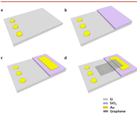
The manufacture of the GDS is illustrated in Figure 1. First, electrodes were formed on silicon substrates using a shadow
mask as shown in Figure 1a. In order to form ohmic contacts between source electrodes and silicon substrates, the native silicon oxide layer was removed by immersion in 3% diluted hydrofluoric acid (HF) for 30 s followed by deposition of titanium/gold (Ti/Au) = 20/80 nm using a shadow mask with a radius of 1 mm. These electrodes operate as the source for the n-type silicon (n-Si) and the drain for the p-type silicon (p-Si) GDS devices, respectively. A layer of 150 nm SiO2 was deposited onto the silicon substrates with a metal shadow mask to prevent direct currentflow from source to drain electrodes (Figure 1b), followed by deposition of Ti/Au = 20/80 nm as a drain (source) electrodes (Figure 1c). Chemical vapor deposition (CVD) growth yielded a continuous layer of predominantly monolayer graphene with an area of close to 1 cm214. The graphene film was transferred on top of the Si/ SiO2/Ti/Au structure after HF dipping to remove the native oxide layer from the exposed silicon area. Careful transfer ensured that the graphene layer connected the gold pad on the SiO2 insulator layer to the bare silicon, without touching the
electrodes directly connected to the silicon layer, as indicated in Figure 1d, and the PMMA layer was dissolved in warm acetone. Electrical measurements were done with a Suess probe station with a Keithley 2612A source meter. Gas sensing was carried out in a custom-made gas sensing chamber. The samples were bonded on a chip carrier which was connected via pressure probes to a Keithley 2612A sourcemeter for electrical read out. Ammonia (NH3) in various concentrations with dry nitrogen (N2) as carrier gas was injected with a flow of 100 sccm at 10 Torr. Raman spectra were taken with a Witec Alpha 300 Raman microscope with a 532 nm excitation wavelength. Scanning electron microscopy (SEM) was carried out in a Zeiss Ultra Plusfield emission SEM at 2 keV.
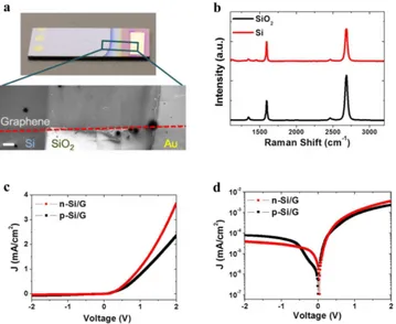
A photograph of a fabricated chip, with source and drain contacts clearly visible, is shown in Figure 2a. The scanning electron microscopy (SEM) image shows the region between SiO2 and Si bridged by graphene. The image was stitched together from eight SEM micrographs and approximately represents the area indicated on the optical image. Some polymer residue from the transfer process is visible. The graphene covered an area of approximately 6.44 mm2on the n-Si and 9.87 mm2on the p-Si silicon substrate, representing the active areas of the GDS’s.
Raman spectroscopy was used to assess the quality of the graphene. Figure 2b shows Raman spectra of graphene on SiO2 and Si. The principal peaks observed in graphene are the G peak at 1590 cm−1and the 2D peak at 2680 cm−1. The peak intensity ratio (I2D/G) of ∼2.3 and the 2D peak width of ∼35 cm−1 both indicate monolayer graphene. A small D peak observed at 1340 cm−1is indicative of the presence of some defects or polymer residue.
Figure 2c shows the current density−voltage (J−V) characteristics of GDS's with n-Si and p-Si substrates, respectively, measured at room temperature. To keep the same bias polarity, a positive bias voltage was applied to the drain electrode in the n-Si GDS, and conversely, a negative bias voltage was applied to the drain electrode in the p-Si GDS. The devices exhibit the typical rectifying behavior of a Schottky diode. One can assume that the graphene is fully electrically intact and well contacted by the gold pad, and therefore transport is dominated by the graphene/silicon interface.15,16 The behavior of a Schottky diode can be described using thermionic emission theory in which the J−V relationship is given by:16
η = − ⎡ ⎣ ⎢ ⎢ ⎛ ⎝ ⎜ ⎞ ⎠ ⎟ ⎤ ⎦ ⎥ ⎥
J J qV
k T
exp 1
s
D
B (1)
whereηis the ideality factor,qis the electronic charge,kBis the Boltzmann constant, Tis the absolute temperature, VD is the voltage applied across the junction, and Js is the reverse saturation current density, which can be expressed by:
ϕ = * ⎛− ⎝ ⎜ ⎞ ⎠ ⎟
J AA T q
k T exp
s
2 B
B (2)
where A is the effective area of the diode contact, A* is the Richardson constant which is equal to 112 A cm−2K−2for n-Si and 32 A cm−2K−2for p-Si, andϕ
Bis the SBH of the diode. 15
[image:2.625.59.299.280.479.2]The ideality factor of a diode is a measure of how closely it follows ideal behavior on a logarithmic scale and has a value of unity in the ideal case.
Figure 1.Fabrication process of a GDS. (a) The source electrodes are deposited immediately after native silicon oxide removal to give ohmic contacts. (b) A 150 nm SiO2 insulation layer is deposited by sputtering. (c) The drain electrode is deposited on SiO2. (d) Graphene is transferred after removal of the native oxide from Si.
In practice there are second-order effects giving rise to deviations from this simple diode description. This is visible in the high bias region where the GDS’s deviate from the initial linear behavior due to the presence of a linear or nonlinear series resistance.17 There are several contributions to this, including the resistance of the graphene and the silicon substrate, contact resistances of the source and drain electrodes, and interface states at the Schottky junction.17,18 In an equivalent circuit model these effects are taken into account with the introduction of a series resistance,Rs, so that the GDS can be described with the ideality factor,η, and the resistance Rs.15 Using Cheung’s function ϕB, can also be extracted.19 Details of the modeling can be found in Supporting Information for device parameter extraction.
From the results of theJ−Vmeasurements and their analysis with the equivalent circuit model,ηandRswere determined to be 1.41, 4.00 kΩfor the n-Si GDS and 1.31, 5.38 kΩfor the p-Si GDS.ϕBwas found to be 0.79 and 0.74 eV for the n-Si and p-Si GDS, respectively. The ideality factor for the n-Si GDS is much improved on that initially reported11 and matches the values recently reported by Miao et al.20 The values match those of Schottky barrier diodes between carbon thinfilms and silicon substrates reported by Yim et al.,21where the interface was engineered with great care. However, it is higher than the value of 1.1 reported by Yang et al.,13 even though their electrical response appears to be very similar to that reported here. This discrepancy might be due to the fact that fewer data points were used in theirfitting procedure.
Following on from our initial diode characterization we exposed the GDS, with its bare graphene surface, to various liquids. The liquids were directly applied onto the devices using
a pipet. The droplet volume was typically 60−120μL, covering the entire graphene/Si area, as shown in figure S1 in Supporting Information. The analytes were exchanged by rinsing the chip with solvent and blow-drying with nitrogen. When the GDS response drifted it was recovered using the procedure outlined below.
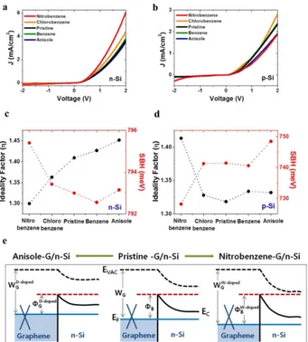
[image:3.625.135.494.67.361.2]determined by the SBH, chemical modification of the graphene directly controls the current across the graphene/semi-conductor interface. Thus, the obtained electrical data is in
[image:4.625.143.484.65.443.2]agreement with the modulation of the SBHs due to chemical doping of the graphene and can be used to evaluate the doping behavior of liquids and gases.25 Similar changes in the Figure 3.Effects on n-Si and p-Si GDS's exposed to various aromatic molecules.J−Vof (a) n-Si GDS and (b) p-Si GDS. Variation of the ideality factorηand Schottky barrier heightϕBof (c) n-Si GDS and (d) p-Si GDS. (e) Schematic band diagram of the graphene/n-Si interface with EDs (left), pristine state (middle), and EAs (right).EVAC,EC,WG, andϕBindicate the vacuum energy, conduction band, graphene work function, and Schottky barrier height, respectively.
Figure 4.Change ofRsin GDS exposed to various aromatic molecules. (a) Variation of the series resistance (Rs) for n-Si and p-Si GDS's upon exposure to liquid aromatic molecules. (b)Rsof the n-Si GDS as a function of the concentration of anisole in benzene.
[image:4.625.64.548.498.689.2]electronic structure of single wall carbon nanotubes5,26 and graphene10,27upon exposure to solvents have previously been reported. The modification of the current is small compared to gate induced doping, as reported in ref 11, and may not account completely for the observed modulation of the GDS.
We also extracted the series resistance values for the GDS’s from plots of dV/dJ vs 1/J (see Figure S2a in Supporting Information for the pristine GDS’s). Upon exposure to liquid aromatic molecules as shown in Figure 4a, Rs increased with EDs, whereas it decreased with EAs, independent of the substrate type. As pristine graphene in ambient conditions displays p-type behavior caused by adsorbed moisture or oxygen,24EAs introduce additional holes as charge carriers to the graphene, further reducing its sheet resistance.28 On the contrary, EDs supply electrons to the graphene, bringing it closer to its charge neutrality point, effectively increasing its sheet resistance.
This can be used to determine the concentration of EAs or EDs in a neutral solvent. A plot of the series resistance variation as a function of anisole concentration in benzene is shown in Figure 4b. The series resistance increases linearly with increasing anisole concentration, and the relationship can be described as
= × + Ω
Rs [4.1 n(%) 3863] (3) wherenis the concentration of anisole. The sensitivity of the n-Si GDS is 4.1Ωfor a percentile concentration of anisole.
The GDS can also be used to determine the extent of charge transfer from gaseous molecules to graphene. The doping behavior of graphene and related systems has been intensively studied for gas sensing applications. One NH3 molecule has been predicted to induce 0.03 electrons onto graphene,29 similar to the case of carbon nanotubes.30
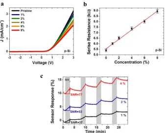
Figure 5a shows theJ−Vcurves of the p-Si GDS after 5 min of ammonia (NH3) exposure with concentrations from 0 to 8% in Ar. It is clearly visible that the current levels drop with increasing ammonia concentration. Using the equivalent circuit model, series resistance values were extracted as shown in Figure 5b. The resistance value of the GDS scales linearly with NH3concentration in this regime and can be described as
= × + Ω
Rs [425.7 n(%) 5552] (4) wherenis the concentration of NH3. Thus the resistance value of the p-Si GDS changes by 425.7Ωpercent concentration of NH3, which is well distinguishable. The time dependent sensor response of the n-Si GDS is shown in Figure 5c, where the resistance changes are recorded upon repeated NH3injections (gray boxes) at various concentrations. There is an immediate response toward change in the gas atmosphere. It is important to note that the observed delay is mainly due the large volume of our sensing chamber and the slight drift is due to incomplete recovery between measurements. The sensing performance is generally evaluated by percentile resistance change depending on time. The sensor responseΔRwas normalized to the initial resistance,R0, before NH3exposure. This is defined as sensor response (S) and given by
= Δ × Δ = −
S R
R0 100(%) R Rg R0 (5) where Rg and R0 are resistances with and without NH3, respectively.
[image:5.625.146.484.65.338.2]previously reported.6,30,31The recovery time can be accelerated by vacuum annealing and UV illumination in fully integrated sensors.4,30,32
The signal-to-noise ratio (SNR) of the GDS is 37 for exposure to 1% NH3. For comparison, we fabricated a graphene-based chemiresistor device. Measuring the resistivity change in two-point configurations for graphene grown under similar conditions gave a SNR of 32 at 10% NH3(see Figure S3 in Supporting Information for sensor response of graphene FETs). Thus the GDS structure leaves room for detection at much lower concentrations, when the graphene and device structures are optimized.
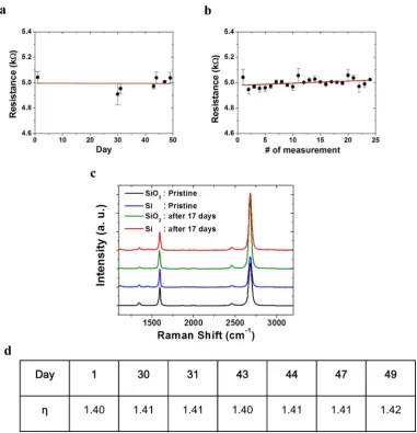
Generally, recovery is a key factor in sensing applications. After exposure to various chemicals, the GDS's were immersed in warm acetone followed by rinsing with IPA and a baking at 200 °C in ambient to remove residues. Figure 6a shows 24 different measurements of the resistance of a n-Si GDS conducted after this procedure. The variation of the resistance is within 2%, demonstrating the high repeatability of the device. Moreover, the long-term stability of the n-Si GDS was tracked over time by measurement after recovery, as shown in
Figure 6b. The resistance value was extracted under a bias of +1 V from dV/dJvs 1/Jand varied by less than 1.1% over 49 days. The ideality factor also shows no significant change over 49 days, as shown in Figure 6c. Raman spectra were obtained before and after the measurement of several chemicals, including ammonia, followed by the recovery procedure. No obvious change in the spectra was apparent, confirming negligible degradation of the device following sensing and recovery as shown in Figure 6d. This long-term stability and resilience to a number of chemicals including aromatic molecules, NH3, and aqueous solutions shows the incredible robustness of graphene, an important prerequisite for sensor applications.
[image:6.625.122.504.64.460.2]High-performance Schottky barrier diodes were fabricated using graphene on n- and p-type silicon substrates. For detailed analysis diode parameters such as ideality factor, SBH, and series resistance were extracted using an equivalent circuit model. These parameters show a marked improvement on values reported before, especially in the case of the p-Si GDS. Furthermore, we present tuning of the rectifying characteristics of GDS's through chemical modification. Our device design Figure 6.Repeatability and long-term stability of GDS's. (a) The resistance change over repeated measurement of the n-Si GDS after exposure to various chemicals followed by recovery. The resistance values were extracted under a bias voltage of +1 V. (b)Rsof n-Si GDS over 49 days taken after recovery procedure. (c) Comparison of Raman spectra of transferred graphene before experiments (pristine) and 17 days after exposure to various analytes. This implies negligible degradation of the graphene following sensing and recovery. (d) The ideality factor of the n-Si GDS over 49 days measured after recovery.
allowed for charge transfer from adsorbents to graphene to be investigated, exploiting the monolayer nature of graphene as a sensor. Changes in the SBH andRsvalues of the GDS could be directly linked to the work function and conductivity of the graphene. The chemical tuning of graphene can be further exploited for graphene based devices. The GDS configuration, with its bottom contact, has proven to be extremely robust, allowing recovery of the device after exposure to various chemicals, an important prerequisite for a new sensor platform. Using the GDS, it was possible to measure the effect of charge transfer from liquids and gases and quantify their concentration. The ability to extract a number of parameters (ideality factor, SBH, andRs) from one GDS and the possibility of creating various GDS's by using semiconductor substrates with different doping levels affords the opportunity to use multiparameter data analysis to extract principal components, that is, identify different species based on specific responses of the GDS. This would remove the necessity of functionalizing graphene to engender selectivity, which often has a negative impact on the quality of the graphene and the stability of the device response. Further investigation of diode-type graphene devices toward doping of graphene and multiparameter sensing is ongoing. The simple and robust nature of the device design mean that it could be analogously fabricated using other 2D materials, potentially giving selectivity in sensing applications.
■
ASSOCIATED CONTENT*
S Supporting InformationAdditional experimental details, details of data analysis and comparative sensing data with GFETs. This material is available free of charge via the Internet at http://pubs.acs.org.
■
AUTHOR INFORMATIONCorresponding Author
*E-mail: [email protected]. Notes
The authors declare no competingfinancial interest.
■
ACKNOWLEDGMENTSThis work was supported by the SFI under Contracts No. 08/ CE/I1432, PI_10/IN.1/I3030 and by the EU under FP7-PPP Electrograph (Con. No. 266391) and NMP-ICT GRAFOL (Con. No. 285275). The authors thank Christian Wirtz and Hugo Nolan for discussions and artwork and the AML for microscopy support.
■
REFERENCES(1) Schottky, W.Naturwissenschaften1938,26(52), 843−843. (2) Mott, N. F.Math. Proc. Cambridge Philos. Soc. 1938,34 (04), 568−572.
(3) Castro Neto, A. H.; Guinea, F.; Peres, N. M. R.; Novoselov, K. S.; Geim, A. K.Rev. Mod. Phys.2009,81(1), 109−162.
(4) Schedin, F.; Geim, A. K.; Morozov, S. V.; Hill, E. W.; Blake, P.; Katsnelson, M. I.; Novoselov, K. S.Nat. Mater.2007,6(9), 652−655. (5) Kauffman, D. R.; Star, A.Analyst2010,135(11), 2790−2797. (6) Kong, J.; Franklin, N. R.; Zhou, C.; Chapline, M. G.; Peng, S.; Cho, K.; Dai, H.Science2000,287(5453), 622−625.
(7) Chen, C. W.; Hung, S. C.; Yang, M. D.; Yeh, C. W.; Wu, C. H.; Chi, G. C.; Ren, F.; Pearton, S. J.Appl. Phys. Lett. 2011,99 (24), 243502−3.
(8) Daly, R.; Kumar, S.; Lukacs, G.; Lee, K.; Weidlich, A.; Hegner, M.; Duesberg, G. S.J. Sensors2012, 219485.
(9) Yavari, F.; Koratkar, N.J. Phys. Chem. Lett.2012,3(13), 1746− 1753.
(10) Newaz, A. K. M.; Puzyrev, Y. S.; Wang, B.; Pantelides, S. T.; Bolotin, K. I.Nat. Commun.2012,3, 734.
(11) Chen, C.-C.; Aykol, M.; Chang, C.-C.; Levi, A. F. J.; Cronin, S. B.Nano Lett.2011,11(5), 1863−1867.
(12) Tongay, S.; Schumann, T.; Miao, X.; Appleton, B. R.; Hebard, A. F.Carbon2011,49(6), 2033−2038.
(13) Yang, H.; Heo, J.; Park, S.; Song, H. J.; Seo, D. H.; Byun, K.-E.; Kim, P.; Yoo, I.; Chung, H.-J.; Kim, K. Science 2012, 336 (6085), 1140−1143.
(14) Kumar, S.; McEvoy, N.; Kim, H.-Y.; Lee, K.; Peltekis, N.; Rezvani, E.; Nolan, H.; Weidlich, A.; Daly, R.; Duesberg, G. S.Phys. Status Solidi B2011,248(11), 2604−2608.
(15) Sze, S. M.; Ng, K. K.Physics of Semiconductor Devices; Wiley: New York, 2006.
(16) Rhoderick, E. H.; Williams, R. H.Metal-Semiconductor Contacts; Clarendon Press: London, 1988.
(17) Keffous, A.; Siad, M.; Mamma, S.; Belkacem, Y.; Lakhdar Chaouch, C.; Menari, H.; Dahmani, A.; Chergui, W.Appl. Surf. Sci.
2003,218(1−4), 337−343.
(18) Tung, R. T.Phys. Rev. B1992,45(23), 13509−13523. (19) Cheung, S. K.; Cheung, N. W.Appl. Phys. Lett.1986,49(2), 85−87.
(20) Miao, X.; Tongay, S.; Petterson, M. K.; Berke, K.; Rinzler, A. G.; Appleton, B. R.; Hebard, A. F.Nano Lett.2012,12(6), 2745−2750. (21) Yim, C.; McEvoy, N.; Rezvani, E.; Kumar, S.; Duesberg, G. S.
Small2012,8(9), 1360−1364.
(22) Xia, F.; Farmer, D. B.; Lin, Y.-m.; Avouris, P.Nano Lett.2010,
10(2), 715−718.
(23) Zhang, W.; Lin, T.; Liu, K.-K.; Tite, T.; Su, Y.; Chang, C.-H.; Lee, Y.-C.-H.; Chu, C.-W.; Wei, K.-C.-H.; Kuo, J.-L.; Li, L.-J.ACS Nano
2011,5(9), 7517−7524.
(24) Novoselov, K. S.; Geim, A. K.; Morozov, S. V.; Jiang, D.; Katsnelson, M. I.; Grigorieva, I. V.; Dubonos, S. V.; Firsov, A. A.
Nature2005,438(7065), 197−200.
(25) Wu, Y.; Perebeinos, V.; Lin, Y.-m.; Low, T.; Xia, F.; Avouris, P.
Nano Lett.2012,12(3), 1417−1423.
(26) Shin, H.-J.; Kim, S. M.; Yoon, S.-M.; Benayad, A.; Kim, K. K.; Kim, S. J.; Park, H. K.; Choi, J.-Y.; Lee, Y. H.J. Am. Chem. Soc.2008,
130(6), 2062−2066.
(27) Dong, X.; Fu, D.; Fang, W.; Shi, Y.; Chen, P.; Li, L.-J.Small
2009,5(12), 1422−1426.
(28) Das, B.; Voggu, R.; Rout, C. S.; Rao, C. N. R.Chem. Commun.
2008,0(41), 5155−5157.
(29) Zhang, T.; Nix, M. B.; Yoo, B.-Y.; Deshusses, M. A.; Myung, N. V.Electroanalysis2006,18(12), 1153−1158.
(30) Ko, G.; Kim, H. Y.; Ahn, J.; Park, Y. M.; Lee, K. Y.; Kim, J.Curr. Appl. Phys.2010,10(4), 1002−1004.
(31) Zhang, Y.-H.; Chen, Y.-B.; Zhou, K.-G.; Liu, C.-H.; Zeng, J.; Zhang, H.-L.; Peng, Y.Nanotechnology2009,20(18), 185504.