warwick.ac.uk/lib-publications
Original citation:
Shreejith, Shanker, Cooke, Ryan A. and Fahmy, Suhaib A. (2018) A smart network interface
approach for distributed applications on Xilinx Zynq SoCs. In: International Conference on
Field-Programmable Logic and Applications, Dublin, Ireland, 27–31 Aug 2018. Published in:
Proceedings of the International Conference on Field-Programmable Logic and Applications
Permanent WRAP URL:
http://wrap.warwick.ac.uk/106307
Copyright and reuse:
The Warwick Research Archive Portal (WRAP) makes this work by researchers of the
University of Warwick available open access under the following conditions. Copyright ©
and all moral rights to the version of the paper presented here belong to the individual
author(s) and/or other copyright owners. To the extent reasonable and practicable the
material made available in WRAP has been checked for eligibility before being made
available.
Copies of full items can be used for personal research or study, educational, or not-for profit
purposes without prior permission or charge. Provided that the authors, title and full
bibliographic details are credited, a hyperlink and/or URL is given for the original metadata
page and the content is not changed in any way.
Publisher’s statement:
© 2018 IEEE. Personal use of this material is permitted. Permission from IEEE must be
obtained for all other uses, in any current or future media, including reprinting
/republishing this material for advertising or promotional purposes, creating new collective
works, for resale or redistribution to servers or lists, or reuse of any copyrighted component
of this work in other works.
A note on versions:
The version presented here may differ from the published version or, version of record, if
you wish to cite this item you are advised to consult the publisher’s version. Please see the
‘permanent WRAP url’ above for details on accessing the published version and note that
access may require a subscription.
A Smart Network Interface Approach for
Distributed Applications on Xilinx Zynq SoCs
Shanker Shreejith, Ryan A. Cooke, and Suhaib A. Fahmy
School of Engineering University of Warwick, Coventry, UK
Email:{s.shanker, ryan.cooke, s.fahmy}@warwick.ac.uk
Abstract—Networked embedded systems have seen tremendous growth with many more complex critical and non-critical systems exchanging information over networks of various types. At each node, information is processed by the network stack before the application sees the data. Large portions of the stack are in software, resulting in significant and non-deterministic delays. While hybrid compute platforms like the Xilinx Zynq can accel-erate processing tasks through offloading to programmable logic, the delays incurred due to connectivity can significantly impact overall application latency. In this paper, we present a smart network interface approach for the Xilinx Zynq platform based on datapath extensions within the otherwise standard Ethernet interface. We show that this approach improves computation offload latency by 24–27% and throughput by 37% for a complex computational kernel.
I. INTRODUCTION ANDRELATEDWORK
Cloud computing has gained widespread adoption in sce-narios where data from distributed sources must be collected and processed in order to extract value, such as in industrial equipment monitoring, business analytics, or fraud detection. It allows for more complex or faster computation than is possible at the data sources, and added scalability. However as the amount of data grows, fully centralised computation can lead to significant latencies, and high bandwidth and resource requirements. This is problematic for applications with strict latency or power constraints. Hence, in networked environments connecting a large number of sensors, actuators, and computational resources, decentralisation is becoming more important.
A key challenge when building such a distributed applica-tion is communicaapplica-tion latency. Tradiapplica-tional system architectures abstract away the delay involved in moving data between the application and physical layers. As such, in time-sensitive applications, there has been an attempt to bring computation closer to the network interface. Concepts such as Smart NIC (network interface card) enable computation to be performed very close the the physical medium in a network interface, avoiding a round trip through the processor’s non-deterministic network stack. These have found widespread adoption in ap-plications such as high frequency trading, where large volumes of data received must be reacted to in minimal time.
In this paper we explore an approach for building such architectures on the Xilinx Zynq hybrid FPGA platform, en-abling processing on the integrated Ethernet interface without involving the host processor, thus offering a significant
im-provement in response time over a standard hardware-offload approach. This offers benefits in applications that involve processing large volumes of data within strict time constraints.
Reconfigurable System-on-Chip (SoC) platforms such as Xilinx Zynq and Altera Arria FPGAs are increasingly being deployed in scenarios ranging from small mobile compute platforms (drones and quadcopters) through self-driving plat-forms, to accelerating deep learning. These platforms combine capable ARM cores with tightly coupled programmable logic that can be interfaced through a series of high-throughput interfaces, with an array of networking options built in such as controller area network (CAN) and Gigabit Ethernet (GigE). A common challenge with these platforms is that interconnect performance is largely dependent on low level optimisation of communication between the different parts of the SoC [1]. In most cases, hardware accelerators are integrated as peripherals to the central processor, that then manages all connectivity and offloading to these accelerators. As a result, commodity boards are designed such that external interfaces are connected to the processor interconnect.
Optimisations to data movement in such platforms have been explored including storing data in DRAM (neural net-works/vision systems) [2], high speed reconfiguration enabled by creating a separate path to the configuration controller [3], and separate network interfaces like Ethernet wired directly into the PL. The generality of these interfaces simplifies system design, but also presents a latency challenge that can have a severe adverse effect on the performance gains possible with accelerators.
In [4] the authors use scatter-gather/DMA proxying on the Zynq platform to redirect Ethernet traffic to a custom GigE Vision Bridge implemented on the programmable logic (PL) to perform low-latency image processing on an incoming video stream. We explore proxying alongside the proposed method in Section II.
detection [10].
For alternate network standards like FlexRay and CAN (used primarily in automotive and industrial control applica-tions), data-path extensions have been shown to enable im-proved communication throughput [11], energy efficiency [12], and expanded features [13], [14].
The approach we present in this paper generalises the concept of smart network interfaces on commodity FPGA SoC platforms, proposing a configurable datapath extensions framework for the Xilinx Zynq platform to enable seamless processing of data in a distributed application with minimal latency compared to traditional approaches.
II. ARCHITECTURE A. Traditional Setup
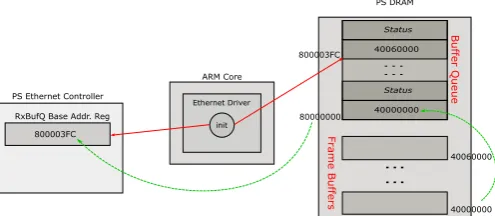
By design, the Ethernet interface on most commodity Xilinx Zynq boards is attached to the processor system (PS), allowing the ARM cores to run operating systems like Linux with a full TCP/IP networking stack, while offloading complex computations to the custom hardware on the programmable logic (PL). The PS Ethernet is initialised during the system initialisation phase, where the Ethernet driver allocates a continuous range of n 64-bit memory locations (where n is configurable) as the Receive Buffer Queue and a set of n
receive buffer locations (calledReceive Buffers). EachReceive Buffer Queue location (called a buffer descriptor) holds the address of the corresponding Receive Buffer and its status. Similarly, theTransmit Buffer QueueandTransmit Buffersare also allocated by the driver during the initialisation phase. The
buffer queuesandbuffersare usually locations in the DRAM memory space. Further, the driver configures the start address of the receive/transmit buffer queues into the base address register of the PS Ethernet controller.
When a packet is received at the Ethernet interface, it is temporarily placed into its internal receive buffer until it is received completely without errors. The controller then looks up the next receive descriptor and initiates a DMA transfer to the buffer location specified by the descriptor and clears itsemptystatus word to mark that a frame is available at the buffer location. The software running on the ARM cores keep track of the buffer status word either through polling or via interrupt, and if a frame is available, the processor fetches the frame and passes it to the software stack or application for decoding. The flow works in the reverse direction when the transmit operation is enabled – the processor initialises the buffer location and clears the empty flag, the Ethernet DMA monitors the flag and initialises a transmission by copying the frame to its internal buffer and setting the empty flag. Fig. 1 shows the setup process. The disadvantage of this approach is that the processor is involved in handling every packet that enters or leaves the system.
B. Hardware Offload via Software
The processor can offload a task into hardware, requiring the data to be moved into the PL, usually via DMA. However, this can introduce non-deterministic latency if the processor is
... ...
PS Ethernet Controller
PS DRAM
... ...
40060000
40000000 Status
Status
RxBufQ Base Addr. Reg 800003FC
40060000
40000000 80000000
800003FC
Ethernet Driver
init
ARM Core
Buffer Queue
[image:3.595.306.554.51.159.2]Frame Buffers
Fig. 1: Initialising the buffer descriptors in the system initial-isation phase for the Zynq PS Ethernet.
occupied with higher-priority tasks when a packet is received. Alternatively, the PS Ethernet block can forward received packets directly into the PL through DMA proxying. To achieve this, during system design, memory spaces are mapped in the PL logic that replicate the buffer queue descriptors (as registers) and buffer memory (BRAMs or FIFOs), mapped as addressable locations via the GP port for the Ethernet DMA controller. To redirect packets back to DRAM, a DMA controller may be instantiated within the PL to copy the frame into the DRAM memory via the high performance (HP) port. On system startup, the driver initialises the PL buffer memory addresses and base address of PL buffer queue into the buffer queue and buffer queue base address register of the Ethernet controller, causing the Ethernet DMA to write the incoming frames into the PL buffer memory. Unpacking logic in the PL checks the frame-type and forwards it to processing logic or PS DRAM for software driven processing. However, the processor is still involved in decision making (based on packet headers), resulting in non-deterministic latencies.
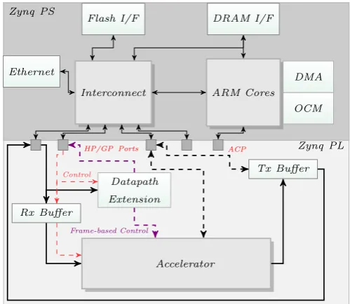
C. Smart Network Interface
Zynq PL Zynq PS
ARM Cores
OCM DMA Interconnect
HP/GP Ports ACP
DRAM I/F Flash I/F
Ethernet
Datapath
Extension
Accelerator Rx Buffer
Tx Buffer
[image:4.595.308.546.48.158.2]Frame-based Control Control
Fig. 2: High-level architecture of the data-path extension approach that mimics an Ethernet SmartNIC on the Zynq PL. Also shown are the various data/control paths between the data-path extension, PS, and hardware accelerator blocks. before but only requires initialisation from software. In regular operation, it requires little to no interference from the software application, and thus offers deterministic and reliable latencies. A high-level overview of the architecture that incorporates data-path extensions in the regular Ethernet packet flow is shown in Fig. 2. The data-path extension is configurable packet monitoring logic that can detect specific patterns in the header/data segment of an Ethernet frame. A control-register stack within the extension block holds a set of configurations that are programmed by the PS. These register bits determine the operation of the extension, specify the pattern to look for in layer-2/layer-3 headers as well as the actions to be performed in case of a match. The logic monitors packets as they arrive through the Zynq’s GP port while the packet is buffered in the RX Buffer. A matching pattern in the incoming frame determines the path taken by the it: to be processed within the PL, ignored without action, or forwarded to the PS for further processing. In the latter case, the extension performs a write into the DRAM logic, and interrupts the processor to take further action, while the processed header information can be read via the register interface. If a packet is to be processed by accelerator(s) in hardware, the extension redirects it into the corresponding path in the PL. We have also incorporated a pathway to send Ethernet frames from the PL: here the frame data can be copied from the PS DDR, packed into an Ethernet layer-2/layer-3 frame and pushed out for transmission via the PS Ethernet (set up from the PS by configuring the transmit ring buffers to mapped locations on PL). This allows the accelerator to process a series of frames to produce results which can be packed into Ethernet frames and sent back out onto the network.
Fig. 3 shows the detailed building blocks and the
Rx Buffer Pattern Checker
Decision Logic Control Registers
Packet Arbiter From
PS (GP)
CFAR Detector
DMA
PS DRAM (HP Port)
Tx Arbiter
Tx Buffer
From PS Ethernet
To PS Ethernet
Fig. 3: The building blocks of the data-path extension logic integrated with the acceleration logic in the PL.
data/control flow paths of the extension logic. As the bytes of the incoming frame are written into the Rx Buffer, the packet checker accumulates 4/8/16 words of the incoming stream into a shift register and tries to match it with the patterns configured in the control registers. The depth of the shift register is a design time parameter (up to 64 Bytes) and can be altered before building the design using the Xilinx tools. The run-time depth is controlled through the configuration in the control stack to match any combination of bytes, as required by the application. The match can be on the frame header segment (i.e., layer-2/layer-3 headers), application data (data-layer headers) or a combination of these. If a combination match is found, the decision logic determines the action to be performed and maps that as the control logic for the packet arbiter.
[image:4.595.42.292.49.266.2]registers) and sets the ready signal to enable transmission via the PS Ethernet interface. The FIFOs within the Rx and Tx Buffer blocks are double-buffered to allow overlap between reception/transmission and processing/framing operations. The architecture can be extended to support multiple accelerators, and configuration matches by setting the high-level parameters at design time.
III. EXPERIMENTS
To evaluate the proposed approach, we use a case study of a LIDAR-based object detection system that forms part of the autonomous driving capabilities and adaptive cruise control system in a modern car [15], [16]. For our exper-iment, we have designed the system to receive sensor data frames over Ethernet and apply the Constant False Alarm Rate (CFAR) detection technique to determine the position and distance of objects. The design targets the Xilinx ZC702 board hosting a Xilinx Zynq XC7Z020 (and can be trivially ported to a Zedboard). The sensor frames data into Ethernet packets containing 512 samples of of data (16-bits), embedded within a data-layer protocol that uses an 8-byte identifier. Two such frames are used in one compute cycle of the CFAR algorithm. The test evaluates the latency incurred by the data-path when processing in the traditional fashion (frame received and processed in PS), offload model (frame received in PS, computation offloaded to PL) and the proposed smart network interface approach.
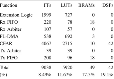
The CFAR algorithm computes the Fast Fourier Transform (FFT) of the incoming samples, followed by a detection chain to determine the presence of an obstruction as well as the distance towards it. On the PL, this is implemented using Xilinx IP cores and fully pipelined custom logic allowing each part of the computation to be completely overlapped. On the PS, we use optimised C code for computing the FFT and the intermediate results are stored in On-Chip Memory (OCM) to minimize compute latency. Table I shows the resources con-sumed by the extension logic (pattern checker, decision logic, and control registers), other blocks of the packet movement system (DMA, arbiter) and the optimised CFAR module. The resources correspond to a parameter configuration allowing three possible pathways for each packet (accelerator, DMA, bypass), 8-word detection shift registers, double buffer FIFOs with each buffer capable of holding full frames and 4-byte wide registers in the control register. Table I shows that the smart interface extensions consume less than 14% of the resources (BRAMs) on the modest Zynq XC7Z020 device.
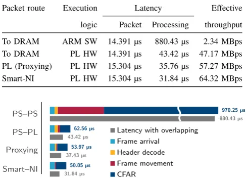
[image:5.595.332.528.65.200.2]We measure the path and processing latency when the packets are handled by the PS, a combination of PS and PL, PL through DMA proxying, and the Smart-NI. The results of our measurements are shown in Table II, recording the packet latency (for each CFAR packet), the CFAR processing latency and the maximum effective throughput achievable in each case. To minimise overheads, we use layer-2 Ethernet packets in the test and the measurements were averaged over 256 frames, each containing CFAR header-bytes and sensor data as the payload. The packet route column specifies the
TABLE I: Resource Consumption on Xilinx Zynq XC7Z020.
Function FFs LUTs BRAMs DSPs
Extension Logic 1999 727 0 0
Rx FIFO 220 78 18 0
Rx Arbiter 107 57 0 0
PL-DMA 538 692 3 0
CFAR 4067 2715 10 42
Tx Arbiter 39 39 0 0
Tx FIFO 208 96 18 0
Total 9038 5920 49 42
(%) 8.49% 11.67% 17.5% 19.1%
destination address set in the PS Ethernet DMA controller (either to PS DRAM or to the memory mapped location in PL), and the execution logic column specifies whether the CFAR processing is done in software on the ARM (ARM SW) or by the custom logic in the PL (PL HW).
Forwarding packets into the PL adds around a 1 µs addi-tional delay compared to moving packets to PS DRAM. This difference is partly due to the low-throughput interface used by the DMA controller (GP port instead of HP port) and partly due to the interrupt scheme, wherein the PL interrupts the processor only after a complete reception of the packet, while the Ethernet DMA controller can mark completion of write to DRAM even before the write into DRAM is completed.
The main difference is the processing latency. Software pro-cessing incurs a large latency as it involves moving significant data (read two data frames, FFT twiddle factors), performing the FFT operation and running detection logic on the FFT output array. Some of these tasks can be overlapped and the measurements in Table II reflect the best case scenario where data movement, frame decoding and frame receptions can be overlapped to reduce the effective latency and the packet reception interrupt is the only interrupt source in the system. In this best case scenario, the maximum throughput achievable using the purely PS approach (reception and processing) is limited by the processing latency to around 2.3 MB/s.
TABLE II: Packet latency and throughput via PS and PL.
Packet route Execution Latency Effective
logic Packet Processing throughput
To DRAM ARM SW 14.391 µs 880.43 µs 2.34 MBps To DRAM PL HW 14.391 µs 43.42 µs 47.17 MBps PL (Proxying) PL HW 15.304 µs 35.76 µs 57.27 MBps
Smart-NI PL HW 15.304 µs 31.84 µs 64.32 MBps
Smart–NI Proxying PS–PL PS–PS
50.05µs 53.97µs 62.56µs
970.25µs
Latency with overlapping Frame arrival
Header decode Frame movement CFAR
31.84µs 37.43µs
43.42µs
[image:6.595.46.288.66.247.2]880.43µs
Fig. 4: Component contributions to overall latency for different approaches. Worst-case latency shows all components, while those that can be overlapped can reduce overall latency.
Fig. 4 shows the breakdown of the different components of the latency in the system for the different scenarios. The PS– PS scenario shows the traditional approach, where processing contributes significantly to the overall latency and data move-ment is also a significant contributor. Overlapping offers a nearly 90 µs reduction in latency. The PS–PL scenario shows a significant reduction in processing time, and overlapping header processing and data movement offers a nearly 20 µs re-duction in overall latency. With Proxying, the frame is received in the PL where a processing block forwards the frame header to PS for decision making, while the data segment is buffered within the PL to minimise data movement (for PL processing), reducing overall latency. Overlapping the reception, header decode, and data movement with CFAR computation results in a reduction of nearly 16 µs in overall latency. Finally the Smart–NI approach, where the frame is received and processed in the PL, maximum gain is achieved when the double-buffering can be effectively utilised, achieving complete over-lapping of reception and CFAR processing. Note that the latency incurred by the PS-Ethernet controller and the slow interconnect channels can be overcome through a dedicated PL Ethernet interface (through an expansion interface like FMC) and soft MAC cores in the PL, while also enabling significant improvements via the Smart-NI extensions by integrating them tightly within the MAC cores. However, the proposed approach is completely general and can be applied to any Zynq platform.
IV. CONCLUSION
Hybrid fully-programmable architectures like the Xilinx Zynq platform are key enablers for distributed processing systems that deal with large data volumes and complex pro-cessing. We presented an approach for achieving low-latency processing in connected platforms by enabling compute close to the network layer with data-layer extensions based on the smart network interface concept. We show that this approach
significantly improves overall response time and processing throughput compared to standard hardware-offload techniques. Our case study showed that the smart network interface approach achieves a nearly 37% increase in throughput and 27% reduction in compute latency, which can be replicated in many applications that require complex processing on volume data. In future, we aim to explore these extensions for in-network on-demand accelerators and processing platforms for decentralised systems interconnected by latency sensitive networks like TSN or synchronous Ethernet.
REFERENCES
[1] J. Silva, V. Sklyarov, and I. Skliarova, “Comparison of on-chip com-munications in Zynq-7000 All Programmable Systems-on-Chip,”IEEE
Embedded Systems Letters, vol. 7, no. 1, pp. 31–34, 2015.
[2] Y. Qiao, J. Shen, T. Xiao, Q. Yang, M. Wen, and C. Zhang, “FPGA-accelerated deep convolutional neural networks for high throughput and energy efficiency,” Concurrency and Computation: Practice and
Experience, vol. 29, no. 20, 2017.
[3] K. Vipin and S. A. Fahmy, “ZyCAP: Efficient partial reconfiguration management on the Xilinx Zynq,” IEEE Embedded Systems Letters, vol. 6, no. 2, pp. 41–44, 2014.
[4] M. Geier, F. Pitzl, and S. Chakraborty, “GigE vision data acquisition for visual servoing using SG/DMA proxying,” inACM/IEEE Symposium on
Embedded Systems For Real-time Multimedia (ESTIMedia), 2016.
[5] A. Fiessler, S. Hager, B. Scheuermann, and A. W. Moore, “HyPaFilter-A versatile hybrid FPGA packet filter,” inProceedings of the ACM/IEEE Symposium on Architectures for Networking and Communications
Sys-tems (ANCS). IEEE, 2016, pp. 25–36.
[6] D. Kohler, “A practical implementation of an IEEE1588 supporting Ethernet switch,” in Proceedings of the International Symposium on Precision Clock Synchronization for Measurement, Control and
Com-munication (ISPCS). IEEE, 2007, pp. 134–137.
[7] G. Carvajal, M. Figueroa, R. Trausmuth, and S. Fischmeister, “Atacama: An open FPGA-based platform for mixed-criticality communication in multi-segmented Ethernet networks,” in Proceedings of the Interna-tional Symposium on Field-Programmable Custom Computing Machines
(FCCM), 2013, pp. 121–128.
[8] G. Carvajal, C. W. Wu, and S. Fischmeister, “Evaluation of communi-cation architectures for switched real-time Ethernet,”IEEE Transactions
on Computers, vol. 63, no. 1, pp. 218–229, 2014.
[9] D. V. Schuehler and J. W. Lockwood, “A modular system for FPGA-based TCP flow processing in high-speed networks,” in Proceedings of the International Conference on Field Programmable Logic and
Application (FPL). Springer, 2004, pp. 301–310.
[10] I. Sourdis and D. Pnevmatikatos, “Fast, large-scale string match for a 10 Gbps FPGA-based network intrusion detection system,” inProceedings of the International Conference on Field Programmable Logic and
Application (FPL), 2003, pp. 880–889.
[11] T. Ziermann, S. Wildermann, and J. Teich, “CAN+: a new backward-compatible controller area network (CAN) protocol with up to 16x higher data rates,” inProceedings of the Design Automation and Test in
Europe (DATE) Conference, 2009.
[12] C. Schmutzler, A. Lakhtel, M. Simons, and J. Becker, “Increasing energy efficiency of automotive E/E-architectures with intelligent communi-cation controllers for FlexRay,” in Proceedings of the International
Symposium on System on Chip (SoC), 2011.
[13] S. Shreejith and S. Fahmy, “Extensible FlexRay communication con-troller for FPGA-based automotive systems,” IEEE Transactions on
Vehicular Technology, vol. 64, no. 2, pp. 453–465, 2015.
[14] S. Shreejith and S. Fahmy, “Smart network interfaces for advanced automotive applications,”IEEE Micro, vol. 38, no. 2, pp. 72–80, 2018. [15] J. Saad, A. Baghdadi, and F. Bodereau, “FPGA-based radar signal processing for automotive driver assistance system,” inProceedings of
IEEE/IFIP International Symposium on Rapid System Prototyping, 2009,
pp. 196–199.
[16] F. Meinl, M. Stolz, M. Kunert, and H. Blume, “An experimental high performance radar system for highly automated driving,” inProceedings of the IEEE International Conference on Microwaves for Intelligent