A Thesis Submitted for the Degree of PhD at the University of Warwick
http://go.warwick.ac.uk/wrap/2564
This thesis is made available online and is protected by original copyright. Please scroll down to view the document itself.
Growth and
Characterisation of
Terrace Graded Virtual
Substrates with Si
1-x
Ge
x
0.15 ≤
x
≤ 1.
By
Lee John Nash
This thesis is submitted in partial fulfilment of the requirements towards
the degree of Doctor of Philosophy for work carried out in the
Department of Physics of the University of Warwick.
Growth of terrace graded virtual substrates, pioneered by Capewell (2002),
has been conducted utilising solid-source molecular beam epitaxy (SS-MBE) to
produce structures of higher composition (up to pure germanium) and greater
thickness (up to 20 m) than previously investigated. Terrace grading offers a
number of advantages over more conventional grading techniques which include the
reduction of surface threading dislocation density, reduction of surface roughness and
the possibility of the complete elimination of threading dislocation pile-up. The
closely spaced pile-up of threading dislocations is believed to have a significant
impact on the electrical properties of processed devices, and its elimination is a key
goal in this work.
Numerous terrace graded virtual substrate compositions have been grown and
characterised during the course of this work and, were appropriate, comparison made
with more conventional structures. The complete elimination of threading dislocation
pile-up has been demonstrated at compositions of 30% and 40%, with a reduced
threading dislocation density in comparison to equivalent linear graded structures. A
major reduction in threading dislocation density has been accomplished though post
growth ex-situ annealing at 900ºC for an extend period of time, though the exact
mechanism remains uncertain. The possible role of surface precipitates enabling
reduction of dislocation pile-up and/or density is considered along with the effects of
Table of Contents
Title Page ... i
Abstract ...ii
Table of Contents ... iii
List of Figures ...vii
List of Tables ... xx
Acknowledgements ...xxiv
Declaration ...xxiv
1
Introduction ... 1
1.1 Semiconductor Technology... 1
1.2 MOSFET Scaling ... 1
1.3 Introduction of Strain Engineering ... 3
1.4 Silicon-Germanium Technology ... 6
1.5 Layer Transfer Technology ... 8
1.6 Thesis Aims and Structure ... 9
2
Principles of Epitaxial Growth and Strain Relief ... 10
2.1 Epitaxial Growth ... 10
2.2 Heteroepitaxial Growth ... 13
2.2.1 Germanium Incorporation ... 15
2.2.2 Critical Thickness ... 16
2.3 Exceeding the Critical Thickness and Virtual Substrates ... 19
2.3.1 Burgers Vector Analysis ... 20
2.3.2 Dislocation Motion ... 21
2.3.3 Nature of Dislocations... 25
2.3.4 Silicon and Germanium Crystal System ... 26
2.3.5 Dislocation Nucleation ... 27
2.3.7 Multiplication Mechanisms ... 31
2.3.7.1 Frank-Read Mechanism ... 31
2.3.7.2 Modified Frank-Read Mechanism (MFR) ... 32
2.3.7.3 Self Annihilation of Threading Dislocations in MFR ... 35
2.4 Virtual Substrate Structures ... 36
2.4.1 Constant Composition ... 36
2.4.2 Step Grading ... 37
2.4.3 Linear Grading ... 37
2.4.4 Terrace Grading ... 40
3
Experimental Methods ... 42
3.1 Solid Source Molecular Beam Epitaxy (SS-MBE) ... 42
3.1.1 V90S Growth System and Vacuum Pumping ... 42
3.1.2 Chamber Outgassing ... 45
3.1.3 Substrate Heater and Control ... 45
3.1.4 Electron Beam Evaporators ... 46
3.1.5 Substrate Cleaning In-Situ and Ex-Situ ... 49
3.1.6 In-Situ High Temperature Oxide Desorption... 49
3.2 System Developments ... 50
3.2.1 Electron Induced Emission Spectroscopy (EIES) ... 50
3.3 Nomarski Optical Interference Microscopy ... 54
3.4 Defect Etching... 55
3.5 Transmission Electron Microscopy (TEM)... 57
3.5.1 Sample Preparation... 58
3.5.2 Transmission Electron Microscope Construction ... 60
3.5.3 Operation of the Transmission Electron Microscope ... 61
3.5.4 Two Beam Diffraction Condition ... 63
3.5.5 Energy Dispersive X-ray Spectroscopy (EDS) ... 68
3.6 High Resolution X-ray Diffraction ... 69
3.6.1 The Reciprocal Lattice and Ewald Sphere Construction ... 71
3.6.3 Analysis of an Omega - Omega-2Theta Scan... 75
3.7 Atomic Force Microscopy (AFM) ... 76
3.7.1 Contact Mode... 77
3.7.2 Image Processing ... 79
4
Low Composition Regime (0-25%) ... 80
4.1 Growth Parameters ... 82
4.1.1 15% Linear Graded Virtual Substrates ... 82
4.1.2 25% Terrace Graded Virtual Substrates... 84
4.2 Nomarski Interference Imaging ... 86
4.2.1 15% Virtual Substrate ... 86
4.2.2 25% Virtual Substrates ... 90
4.3 Cross-Sectional Transmission Electron Microscopy (XTEM) ... 92
4.3.1 15% Virtual Substrates ... 92
4.3.2 25% Virtual Substrates ... 96
4.3.3 EDS Results for 25% Terrace Graded Structures... 98
4.4 High Resolution X-ray Diffraction ... 99
4.5 Atomic Force Microscopy (AFM) ... 104
4.6 Schimmel Defect Etching ... 108
4.7 Summary ... 113
5
Medium Composition Regime (30-40%) ... 115
5.1 Growth Parameters ... 116
5.1.1 30% Terrace Graded Substrates with In-Situ Annealing ... 116
5.1.2 30% Terrace Graded Substrates without In-Situ Annealing ... 118
5.1.3 40% Terrace Graded Substrates without In-Situ Annealing ... 119
5.1.4 30% Linear Graded Substrate with In-Situ Annealing ... 119
5.2 Nomarski Interference Images ... 120
5.2.1 Ex-Situ Annealing ... 124
5.3.1 Ex-Situ Annealing ... 129
5.3.2 Energy Dispersive X-ray Spectroscopy (EDS) ... 132
5.4 Atomic Force Microscopy (AFM) ... 132
5.4.1 Ex-Situ Annealing ... 134
5.5 High Resolution X-ray Diffraction ... 135
5.5.1 Ex-Situ Annealing ... 141
5.6 Schimmel Defect Etching ... 145
5.6.1 Exceptionally Low Threading Dislocation Densities... 149
5.6.2 Ex-Situ Annealing ... 151
5.7 Summary ... 156
6
High Composition Regime (60-100%) ... 159
6.1 Growth Parameters ... 161
6.2 Nomarski Interference Imaging ... 164
6.3 Cross-Sectional Transmission Electron Microscopy (XTEM) ... 167
6.4 Atomic Force Microscopy (AFM) ... 177
6.5 High Resolution X-ray Diffraction ... 180
6.6 Schimmel Defect Etching ... 185
6.7 Summary ... 191
7
Conclusion ... 194
7.1 Further Work ... 197
Appendix ... 199
A.1 Modified RCA Wet Chemical Clean ... 199
A.2 Modified Piranha Wet Chemical Clean ... 200
List of Figures
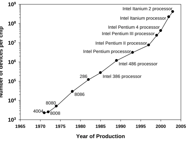
Figure 1.1 – Showing the rising number of transistors contained within
Intel® processors (Intel 2005). ... 2
Figure 1.2 – Schematic representation of an n-MOSFET transistor. ... 3
Figure 1.3 – Schematic representation of the constant-energy ellipses for
unstrained and strained silicon showing the lifting of degeneracy
by the application of tensile strain Takagi et al. (1996). ... 4
Figure 1.4 – Biaxial tensile induced changes in the valence band of silicon
Rim et al. (2003). ... 5
Figure 1.5 – Theoretical prediction of electron (dotted line) and hole (solid
line) mobility enhancement in a strained silicon MOS device
structure under low field conditions Oberhüber et al. (1998). ... 6
Figure 1.6 – A map of band gap versus lattice constant for the III-V alloys
and Si and Ge Fitzgerald et al. (1999). ... 7
Figure 1.7 – Schematic illustration of the layered structure of an SOI
(silicon-on-insulator) wafer. ... 8
Figure 2.1 – Schematic illustration of silicon islands on the Si (001) – (2x1)
surface and the formation of antiphase domain boundaries when
these islands intersect. Antiphase boundaries running parallel
and perpendicular to the dimer rows are denoted AP1 and AP2
respectively. a0 is 3.85Å, the lattice (001) constant of the silicon
(001) surface Bronikowski et al. (1993). ... 11
Figure 2.2 – Schematic representation of a vicinal silicon wafer surface.
The mobile adatoms most easily move along dimer rows and
this direction is indicated with arrows. ... 12
Figure 2.3 – Schematic representation of the growth modes (a) Frank-van
der Merwe (FvM) (b) Volmer-Weber (VW) (c)
Stranski-Krastanov (SK). ... 14
Figure 2.4 – Schematic diagram of the silicon or germanium diamond
crystal lattice. Lattice is fcc with a basis of atoms at (0, 0, 0)
Figure 2.5 – Open circles show experimental data for critical layer thickness
of GexSi1-x alloys vs Ge content x. The misfit varies from 0 to
4.2% at x=1.0. The solid curve gives the present results, as
obtained by energy balance arguments People and Bean (1985). ... 17
Figure 2.6 – Diagram showing elastic distortion of vertical lattice planes in a
morphologically undulating heteroepitaxial layer (w is the
wavelength of undulation) under compressive stress upon its
substrate Cullis (1996). ... 18
Figure 2.7 – The Burgers vector of a dislocation can be determined by
completing a right-handed circuit in a perfect region of crystal
(i) and then making a comparative circuit around the dislocatio n
(ii). The Burgers vector, b, is defined as the vector needed to
close the circuit from start to finish (RH/SF convention). ... 20
Figure 2.8 – Schematic diagram of a threading dislocation propagating
through an epitaxial layer leaving an interface misfit dislocation
behind. ... 22
Figure 2.9 – Diagram illustrating the strain relief provided by an expanding
misfit dislocation as the threading arms glide apart. ... 24
Figure 2.10 – Diagram illustrating the relationship between dislocation
Burgers vectors of the form ½[110], with specific reference to
the (111) glide plane and its intersection with the (001) along the
[-110] line direction. ... 26
Figure 2.11 – Diagrams illustrating how (a) the intersection of an
orthogonally placed misfit dislocation by a moving threading
segment can (b) result in a splitting reaction, if the dislocations
share parallel Burgers vectors. Misfit segments both lie in the
shaded plane with the glide planes for each represented... 30
Figure 2.12 – Schematic cross-sectional representation of a Frank-Read
dislocation source. The central dislocation line marked (a) is
pinned at either end by jog of the dislocation on to different
glide planes marked by the cross and point. Expansion of the
dislocation is shown (b)-(d) until it eventually closes upon itself
(indicated with arrows), whilst the original dislocation returns to
its original state (a). ... 31
Figure 2.13 – Schematic representation of the formation and operation of a
modified Frank-Read multiplication source. Pictures (a) and (c)
show a three dimensional representation whilst (b) and (d) show
a corresponding [1-10] projection. (a) and (b) Two dislocations
with the same 1/2[10-1] Burgers vector cross with a 90º angle in
the plane of the interface. All of the planes and directions are
indicated. The typical annihilation of the intersection is
represented, as well as the bending of one of the corners toward
the substrate resulting from the interaction between the two
corners. In addition a fully formed loop that has intersected the
surface is shown. (c) and (d) Repeated operation of the source
results in a double pile-up of misfit dislocations along the two
glide planes involved in the mechanism LeGoues et al. (1992). ... 34
Figure 2.14 – A graph showing threading dislocation density vs. grading
rate for graded buffers. The cap layers are 1.1 m thick and
32% Ge rich. The straight line corresponds to a 1.1 m thick
uniform (32%) layer. For comparison the results of Fitzgerald et
al. (1992) are also shown contained within the broken rectangle.
Reproduced from a paper by Dutartre et al. (1994)... 38
Figure 2.15 – Schematic diagram showing the pinning of threading
dislocations against a network of misfit dislocations generated
by the modified Frank-Read multiplication mechanism. (a) in
3-D view (b) plan view looking along the [001] direction. ... 39
Figure 2.16 – Schematic cross-sectional diagram viewed along a [110]
direction. In a linearly graded layer (a) the dislocations form
large pile-ups that traverse the layer. In the terrace graded layers
(b) pile-ups are confined in the graded layers and since these
layers are isolated pile-ups do not build throughout the structure.
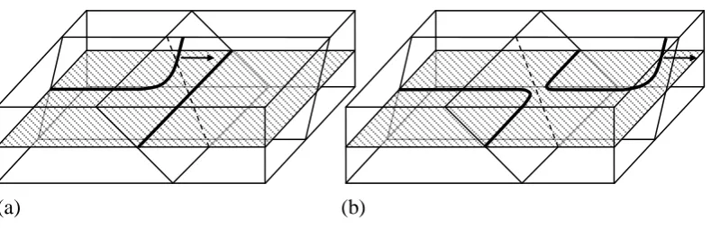
Reproduced with permission (Capewell 2002). ... 40
Figure 3.1 – Schematic of the Vacuum Generators V90S SS-MBE growth
Figure 3.2 – Schematic of electron beam evaporator situated within the
V90S growth chamber. Adapted from an image published by
Kasper et al. (1998). ... 47
Figure 3.3 – Schematic representation (not to scale) of a silicon electron
evaporator and shutter situated inside the V90S UHV growth
system with two sets of Sentinel heads, positioned at the side
and top of the chamber. Also shown is the modified internal
upper water cooling panel allowing line of sight down to the
evaporant source. ... 51
Figure 3.4 – Montage of graphs showing flux rate monitored from the
silicon charge by Sentinel heads in the upper (new) and side
(old) locations, as well as the actual set point and power usage.
(a) Flux feedback control provided from the old Sentinel head
position (b) Flux feedback control provided from the new
Sentinel head position... 53
Figure 3.5 – Schematic representation of a Nomarski optical interference
microscope. ... 54
Figure 3.6 – Example images of etch pit formation after Schimmel etching
around surface threading dislocations (a) at x50 magnification
with interference contrast (b) at x10 magnification without
interference contrast. A threading dislocation is highlighted in
each image by a white circle. ... 57
Figure 3.7 – A series of schematics showing important stages in TEM
sample preparation. (a) initial bonding of epitaxial surfaces
together (b) bonding of additional gash material (c) diamond
sawn section for grinding (d) sample section waxed ready to
grind (e) ground and polished sample with copper support ring
attached (f) final sample structure ready to be ion beamed until
electron transparent. ... 58
Figure 3.8 – Schematic of a Transmission Electron Microscope (TEM) in
(a) bright field imaging mode (b) diffraction imaging mode. ... 61
Figure 3.9 – Schematic diagrams showing (exaggerated) effect of sample tilt
Figure 3.10 – Schematic diagram illustrating the geometric relationship
between the incident electron radiation, atomic lattice planes and
the diffracted beam. ... 64
Figure 3.11 – Reciprocal lattice sections visible in the TEM diffraction
mode when an fcc crystal is viewed along (a) [110] direction
(cross-sectional) (b) [001] direction (plan view). Only selected
lattice points are shown. ... 65
Figure 3.12 – Schematic representation of the origin of Kikuchi lines from
inelastic scattering events. Paired light and dark bands originate
due to net gain and loss in directions that satisfy the Bragg
condition for diffraction. Reproduced from Specimen
Preparation in Materials Science (Goodhew 1972)... 66
Figure 3.13 – Schematic diagram showing the effect of an edge dislocation
on lattice planes in orthogonal directions. Clearly the planes
highlighted in (a) are more distorted by the dislocation than in
(b) and are perpendicular to the dislocations Burgers vector.
Reproduced with kind permission (Capewell 2002). ... 67
Figure 3.14 – Schematic of real space sample tipping with respect to
reciprocal space observed in diffraction mode. Arrows indicate
the respective motions. ... 67
Figure 3.15 – Schematic diagram of a high resolution X-ray spectrometer. ... 69
Figure 3.16 – Schematic representations of a tetragonally distorted cubic
unit cell showing that the (004) spacing is entirely out of plane
whilst the (224) contain components both in plane, ax, and out of
plane, az. ... 70
Figure 3.17 – Diagrams illustrating how a reciprocal lattice is derived from
the real space lattice and how they are related. d1 and d2 are the
spacing between sets of planes 1 and 2 respectively whilst d* are
the corresponding reciprocal lattice vectors. Reproduced from
The Basics of Crystallography and Diffraction (Hammond
2001). ... 71
Figure 3.18 – Ewald reflecting sphere construction for a set of planes at the
Figure 3.19 – Schematic diagrams showing how the Ewald sphere
construction relates to the experimental parameters of the
apparatus. Diagrams are reproduced with kind permission of
Stuart Jollands (University of Warwick, unpublished). ... 73
Figure 3.20 – Schematic diagram of a scanned sample AFM instrument with
the main components indicated. Reproduced from Veeco
training manual (Veeco 2000)... 76
Figure 3.21 – Schematic diagram showing the basic principle of AFM
operation. Movement of the sample beneath the probe causes it
to rise and fall altering the path of the reflected laser light.
Feedback control compensates lowering or raising the sample to
maintain a constant applied force to the surface. ... 77
Figure 3.22 – Scanning electron microscope (SEM) image of a silicon
carbide tipped cantilever AFM probe. Reproduced from Veeco
training manual (Veeco 2000)... 78
Figure 3.23 – Schematic diagrams showing (a) the image profiles of spheres
scanned with a sharp (left) and dull (right) probe (b) Image
profile of trenches scanned with a dirty tip. Reproduced from
Veeco training manual (Veeco 2000). ... 79
Figure 4.1 – Experimental and theoretical enhancement factors of electron
and hole mobility, defined by the ratio of mobility in strained-Si
to unstrained Si MOSFET’s, as a function of composition. Since
the enhancement factor of hole mobility is dependent on Eeff, the
maximum values, typically seen in low Eeff region, are plotted in
this figure. Reproduced from a paper by Takagi et al. (2005). ... 81
Figure 4.2 – Schematic representation of linear graded 15% virtual substrate
specifications showing all possible growth parameter variations
explored. ... 84
Figure 4.3 – Schematic representation of terrace graded 25% virtual
substrate specifications showing the growth parameter variations
explored. ... 85
Figure 4.4 – Nomarski interference images taken at x100 magnification of
Figure 4.5 – An AFM (21x21 m2) image of the slip-band pattern on the
surface of a graded layer with a thickness of 1.5 m and a
Germanium gradient of 15%/ m, grown at 530ºC, after
annealing at 620ºC for 1 hour. Full height scale is 47 nm.
Reproduced from a paper by Shiryaev et al. (1995)... 88
Figure 4.6 – Nomarski interference images taken at x100 magnification of
the terrace graded 25% samples (a) 75037, (b) 75029, and (c)
75036. ... 91
Figure 4.7 – Cross-sectional transmission electron micrographs (in the (220)
two beam diffraction condition) of the linear graded 15%
samples (a) 75027, (b) 75028, (c) 75034, (d) 75031, (e) 75022
and (f) 75030. The surface of the epitaxial layer is near the top
of each image (marked with the upper arrow) and the initial
growth interface below (marked by the lower arrow). ... 93
Figure 4.8 – Cross-sectional transmission electron micrographs (in the (220)
two beam diffraction condition) of the 15% sample 75034. The
surface of the epitaxial layer is near the top of the image
(marked with the upper arrow) with the initial growth interface
below (marked by the lower arrow)... 96
Figure 4.9 – Cross-sectional transmission electron micrographs (in the (220)
two beam diffraction condition) of the 25% samples (a) 75037,
(b) 75029 and (c) 75036. The surface of the epitaxial layer is
near the top of the images (marked with the upper arrow) with
the initial growth interface below (marked by the bottom arrow)
and the top of the first constant composition layer in between
(marked with the middle arrow). ... 97
Figure 4.10 – Omega ( omega-2theta ( 2 scan in the 004 direction
from sample 75028 (15%, 850ºC, 1 m) with phi = 0º. Typical
features found in common between all 15% and 25% structures
investigated... 101
Figure 4.11 – 40 m x 40 m and 10 m x 10 m area atomic force height
Figure 4.12 – A 3-dimensional presentation of a 10 m x 10 m area atomic
force height profile scan for sample 75028 (15%, 850ºC, 1 m)
highlighting the apparent tilt in only one direction. ... 106
Figure 4.13 – 10 m x 10 m area atomic force height profile scans for (a)
75027 (b) 75037. ... 107
Figure 4.14 – 40 m x 40 m area atomic force height profile scans for (a)
75022 (b) 75030 ... 108
Figure 4.15 – Optical micrograph of defect etched sample 75029. The
image was taken in the bright field without interference contrast
at x10 magnification. A surface threading dislocation density of
approximately 4x10⁴/cm2 is revealed by etch pit counting. A
circle highlights an etch pit for clarity. ... 109
Figure 4.16 – Optical micrograph of the surface of sample 75028 (15%,
850ºC, 1 m) after etching with a standard Schimmel etchant for
2 minutes. The arrows indicate the pseudo pile-up with low
threading dislocation density and the circles highlight etch pits
for clarity. ... 111
Figure 5.1 – Schematic representation of 30% virtual substrate
specifications for 75046 (30%, 850-750ºC, In-situ Anneal) high
temperature and 75048 (30%, 700-600ºC, In-situ Anneal) low
temperature. ... 117
Figure 5.2 – Schematic representation of 30% virtual substrate
specifications for 75049 (30%, 850-650ºC Ramping, In-situ
Anneal) intermediate temperature. ... 117
Figure 5.3 – Schematic representation of virtual substrate specifications for
75044 (30%, 800-725ºC Ramping, No Anneal) and 75043 (40%,
800-700ºC Ramping, No Anneal). ... 118
Figure 5.4 – Schematic representation of 30% virtual substrate
specifications for 75055 (30%, 825-725ºC Ramping, No
Anneal). ... 119
Figure 5.5 – Schematic representation of 30% virtual substrate
specifications for a linear graded comparison 76007 (30%,
Figure 5.6 – Nomarski interference images taken at x50 magnification of
samples (a) 75046, (b) 75048, (c) 75049, (d) 75044, (e) 75055,
(f) 75043 and (g) 76007 ... 121
Figure 5.7 – Nomarski interference image taken of sample 75049 at x10
magnification. A disturbance (indicated by arrows) to the
cross-hatch running vertically across the image is believed to be
evidence of threading dislocation pile-up. Circles highlight
localised surface disturbances due to particulate inclusion. ... 123
Figure 5.8 – Nomarski interference image taken at x10 magnification after
an ex-situ anneal has been performed at 900ºC for 15 hours on
samples (a) 75046 and (b) 75048. ... 124
Figure 5.9 – Cross-sectional transmission electron micrographs (in the (220)
two beam diffraction condition) of sample 75046 (a) relatively
thick section (b) relatively thin section. ... 125
Figure 5.10 – Cross-sectional transmission electron micrograph (in the (220)
two beam diffraction condition) of sample 75048. ... 126
Figure 5.11 – Cross-sectional transmission electron micrographs (in the
(220) two beam diffraction condition) of sample (a) 75055 (b)
75043. ... 127
Figure 5.12 – Cross-sectional transmission electron micrograph (in the (220)
two beam diffraction condition) of sample 75046 Annealed at
900ºC for 15 hours. ... 130
Figure 5.13 – Cross-sectional transmission electron micrograph (in the (220)
two beam diffraction condition) of sample 75048 Annealed at
900ºC for 15 hours. ... 131
Figure 5.14 – Cross-sectional transmission electron micrograph (in the (220)
two beam diffraction condition) of sample 75049 Annealed at
900ºC for 15 hours. ... 131
Figure 5.15 – 20 m x 20 m area atomic force height profile scans for (a)
75046 (b) 75048. A possible threading dislocation is indicated
by an arrow in image (b). ... 133
Figure 5.16 – 20 m x 20 m area atomic force height profile scans for (a)
Figure 5.17 – Schematic representation of the dislocation configurations for
the four slip systems of the MFR mechanism. A dislocation
loop has two branches, one gliding on each of the two slip
planes comprising the slip system. The two branches have the
same Burgers vector but different line directions. Reproduced
from a paper by Mooney et al. (1994). ... 138
Figure 5.18 – Schematic diagram representing the Burgers vectors
corresponding to four modified Frank-Read slips systems
(MFR1-4), highlighting their relationships to one another and
the (111) glide plane. ... 139
Figure 5.19 – Schematic diagram illustrating the greater misfit lengths along
orthogonal directions, with strain relief in a direction orthogonal
to the misfit line direction represented by the hatched area. ... 140
Figure 5.20 – High resolution omega ( ) omega-2theta ( 2 ) scan in the
[004] direction from sample 75046 (30%, 850-750ºC, In-situ
Anneal) ex-situ annealed with phi (Φ)=0º. Crosses mark the
central regions of the two distinct peak maxima. ... 144
Figure 5.21 – Optical micrographs of defect etched samples (a) 75046 30%
terrace graded, (b) 75043 40% terrace graded, (c) 76007 30%
linearly graded and (d) 6443 40% linearly graded (externally
grown by LEPECVD)... 147
Figure 5.22 – Graph comparing the surface threading dislocation densities
of terrace graded virtual substrates grown from high temperature
(850ºC) and low temperature (700ºC). ... 150
Figure 5.23 – Optical micrograph of defect etched sample 75048. The
image was taken in the bright field without interference contrast
at x50 magnification. The oval indicates the threading
dislocation pile-up... 151
Figure 5.24 – Time lapse images showing etch pit formation after continued
Schimmel etching (a) 75046 as-grown (b) 75046 ex-situ anneal
at 900ºC for 15 hours. ... 153
Figure 5.25 – Time lapse images showing etch pit formation after continued
900ºC for 15 hours. An arrow indicates a region of threading
dislocation pile-up... 155
Figure 6.1 – Schematic representation of 60% virtual substrate
specifications for 75051 (60%, 500 nm/1 m, 825-650ºC) and
75056 (60%, 1 m/1 m, 825-650ºC). ... 161
Figure 6.2 – Schematic representation of 60% virtual substrate
specifications for 76009 (100%, 1 m/1 m, 825-550ºC). ... 163
Figure 6.3 – Nomarski interference images taken at x50 and x100
magnification. (a) and (b) sample 75056, (b) and (c) sample
75051, (e) and (f) sample 76009. ... 165
Figure 6.4 – Nomarski interference image of sample 75056 taken at x10
magnification. Particulate contamination is highlighted with
white rings. ... 166
Figure 6.5 – Cross-sectional TEM images of sample 75051 (a) (220) two
beam diffraction condition highlighting dislocations (b) (004)
two beam diffraction condition highlighting layer strain.
Arrows indicate the structure surfaces. ... 168
Figure 6.6 – Cross-sectional TEM image of sample 75056 in the (220) two
beam diffraction condition highlighting dislocations within the
structure. An arrow indicates the structures surface. ... 170
Figure 6.7 – Cross-sectional TEM image of sample 75056 in the (004) two
beam diffraction condition highlighting layer strain within the
structure. Light bands spaced throughout sample are 5 nm
silicon spacer layers. An arrow indicates the structures surface... 171
Figure 6.8 – Cross-sectional TEM image of sample 76009 in the (220) two
beam diffraction condition highlighting dislocations within the
structure. Arrows indicate the structures surface. ... 174
Figure 6.9 – Cross-sectional TEM image of upper structure of sample 76009
in the (220) two beam diffraction condition, highlighting
dislocations within the layers. A cascade of dislocations is
initiated at the upper interface of the 50% constant composition
layer. The upper arrows indicate the structures surface and the
Figure 6.10 – Cross-sectional TEM image of upper structure of sample
76009 in the (220) two beam diffraction condition highlighting
dislocations within the layers. A substantial reduction in
dislocation density is evident between the upper interface of the
final graded region and the overlaying germanium cap. ... 176
Figure 6.11 – Atomic force height profile scans of 75051 over an area of (a)
20 m x 20 m (b) 10 m x 10 m. ... 177
Figure 6.12 – Atomic force height profile scans of 75056 over an area of (a)
20 m x 20 m (b) 10 m x 10 m. ... 178
Figure 6.13 – Atomic force height profile scans of sample 76009 over an
area of (a) 40 m x 40 m and (b) 20 m x 20 m. ... 179
Figure 6.14 – Omega ( ) omega-2theta ( 2 ) scans of sample 75056
(60%, 1 m/1 m, 825-650ºC) with phi (Φ) =0º along the (a)
[004] direction (b) [224] direction. Peaks moving right to left
correspond to increasing layer composition, with each peak
resulting from a layer of constant composition... 182
Figure 6.15 – Omega ( ) omega-2theta ( 2 ) scans of sample 76009
(100%, 1 m/1 m, 825-550ºC) along the [004] direction with
(a) Phi (Φ) = 0º (b) Phi (Φ) = 90º. Peaks moving right to left
correspond to increasing layer composition. ... 184
Figure 6.16 – Graph comparing the surface threading dislocation density
between terrace graded virtual substrates grown at high starting
temperature (850ºC). A distinct exponential trend is evident. ... 186
Figure 6.17 – Optical micrograph of the surface of sample 75056 after
etching in a standard Schimmel etch for 3 minutes. Circles
highlight particulate contamination that has resulted in threading
dislocation pile-up, the arrows indicate the direction. ... 188
Figure 6.18 – Optical micrographs of defect etched sample 75051 without
optical interference at (a) x10 magnification (b) x50
magnification. The white arrows indicate the direction of
threading dislocation pile-up. A surface particulate contaminant
Figure 6.19 – Optical micrographs of defect etched sample 75051 without
optical interference at x50 magnification. White arrows indicate
large surface undulations that would appear favourable for
List of Tables
Table 1.1 – Room temperature bulk lattice mobilities of electrons and holes
in unstrained, undoped Si and Ge. Reproduced from a paper by
Schäffler (1997). ... 7
Table 4.1 – A summary of parameter variations explored within the 15%
virtual substrate structures, showing growth temperature and
layer thickness, with the resulting sample labels shown for
reference (grown in numerical order). ... 83
Table 4.2 – A summary of parameter variations explored within the 25%
virtual substrate structures, with the resulting sample labels
shown for reference. ... 85
Table 4.3 – X-ray compositional and relaxation data for the 15% samples
75027, 75028 and 25% sample 75029. Compositional error
±0.5%, relaxation error ±5%. An inherently greater error exists
for the Intermediate layer as no defined peak position exists. ... 99
Table 4.4 – X-ray compositional and relaxation data for the 15% samples
75022 and 75030. Compositional error ±0.5%, relaxation error
±5%. An inherently greater error exists for the Intermediate
layer as no defined peak exists. ... 100
Table 4.5 – Data collected of angular separation (in degrees) in omega
between (004) planes in the silicon substrate and constant
compositional layer for the 15% samples 75027, 75028 and 25%
sample 75029. The error in determination of the angular
separation ± 0.01º... 103
Table 4.6 – Data collected of angular separation (in degrees) in omega
between (004) planes in the silicon substrate and constant
compositional layer for the 15% samples 75022 and 75030. The
error in determination of the angular separation ± 0.01º. ... 103
Table 4.7 – RMS surface roughness and height range measurements
determined from AFM images of the 15% samples 75022,
Table 4.8 – RMS surface roughness and height measurements determined
from AFM images of the 25% samples 75037 and 75029. ... 104
Table 4.9 – Table containing threading dislocation densities for 15% 1 m
layer structured samples 75027, 75034 and 75028 and 200 nm
layered structure 75030, calculated by counting surface etch
pits, accompanied by standard deviations. Standard Schimmel
etching was employed for the 1 m thick samples whilst the
modified Schimmel etch was utilised for the 200 nm sample. ... 110
Table 4.10 – Table containing threading dislocation densities for 25% 1 m
layer structured samples 75037 (only 20% composition
measured) and 75029. Densities calculated by counting surface
etch pits, accompanied by standard deviations. The standard
Schimmel etch was employed. ... 112
Table 5.1 – EDS composition data for samples 75046 (30%, 850-750ºC,
In-situ Anneal), 75048 (30%, 700-600ºC, In-situ Anneal), 75055
(30%, 825-725ºC Ramping, No Anneal) and 75043 (40%,
800-700ºC Ramping, No Anneal). Composition error of ±5%. ... 132
Table 5.2 – RMS surface roughness measurements determined from AFM
images of samples 75046 (30%, 850-750ºC, In-situ Anneal) and
75048 (30%, 700-600ºC, In-situ Anneal) as-grown and annealed
at 900ºC for 15 hours. ... 134
Table 5.3 – X-ray composition and relaxation data for samples 75046 (30%,
850-750ºC, In-situ Anneal) and 75048 (30%, 700-600ºC, In-situ
Anneal). Compositional error no more than ±0.5%, relaxation
error up to ±5%. ... 136
Table 5.4 – Data collected of angular separation in omega between (004)
planes in the silicon substrate and constant composition layers
for samples 75046 (30%, 850-750ºC, In-situ Anneal) and 75048
(30%, 700-600ºC). ... 137
Table 5.5 – X-ray composition and relaxation data for samples 75046 (30%,
850-750ºC, In-situ Anneal), 75048 (30%, 700-600ºC, In-situ
after annealing ex-situ at 900ºC for 15 hours. Compositional
error no more than ±0.5%, relaxation error up to ±5%. ... 141
Table 5.6 – Data collected of angular separation in omega between (004)
planes in the silicon substrate and constant composition layers
for samples 75046 (30%, 850-750ºC, In-situ Anneal), 75048
(30%, 700-600ºC, In-situ Anneal) and 75049 (30%, 850-650ºC
Ramping, In-situ Anneal) after annealing ex-situ at 900ºC for 15
hours. ... 142
Table 5.7 – X-ray composition, relaxation and angular (omega) separation
data for sample 75046 (30%, 850-750ºC, In-situ Anneal)
obtained at higher angular resolution than previous scans.
Compositional error no more than ±0.5%, relaxation error up to
±5%. ... 143
Table 5.8 – Table summarising threading dislocation densities for samples
75046 (30%, 850-750ºC, In-situ Anneal), 75055 (30%,
825-725ºC Ramping, No Anneal), 75044 (30%, 800-825-725ºC Ramping,
No Anneal) and 75043 (40%, 800-700ºC Ramping, No Anneal)
calculated by counting surface etch pits, accompanied by
standard deviations. ... 145
Table 5.9 – Table containing threading dislocation densities for samples
6443 (externally grown LEPECVD) and 76007 (30%, Linearly
Graded, 850-750ºC, In-situ Anneal) calculated by counting
surface etch pits, accompanied by standard deviations. ... 148
Table 6.1 – EDS composition data for 75051 (60%, 500 nm/1 m,
825-650ºC) as well as thickness measurements made from
cross-sectional TEM images. Compositional error of ±10% due to
thickness of sample. Combined layer thickness ± 5%. ... 169
Table 6.2 – EDS composition data for 75056 (60%, 1 m/1 m, 825-650ºC)
as well as thickness measurement made from cross-sectional
TEM images. A calculated composition based upon additional
layer thickness being solely attributed to excess silicon
deposition is also presented. Compositional error of ±10% due
Table 6.3 – EDS compositional data for 76009 (100%, 1 m/1 m, 825
550ºC). Compositional error of ±10% due to thickness of the
sample. ... 173
Table 6.4 – RMS surface roughness and height range measurements
determined from AFM images of samples 75051 (60%,
500 nm/1 m, 650ºC), 75056 (60%, 1 m/1 m,
825-650ºC) and 76009 (100%, 1 m/1 m, 825-550ºC). ... 180
Table 6.5 – X-ray composition and relaxation data for samples 75056 (60%,
1 m/1 m, 825-650ºC) and 76009 (100%, 1 m/1 m,
825-550ºC). Compositional error no more than ±0.5%,
relaxation error ±5%. ... 181
Table 6.6 – Data collected for angular separation in omega between (004)
planes in the silicon substrate and constant compositional layer,
along orthogonal phi (Φ) directions. The error in
determination of the angular separation ± 0.01º. ... 185
Table 6.7 – Table containing threading dislocation densities for samples
75051 (60%, 500 nm/1 m, 825-650ºC) and 75056 (60%,
1 m/1 m, 825-650ºC) calculated by counting surface etch pits
optically at x50 magnification, accompanied by standard
deviations. Standard Schimmel etchant employed. ... 185
Table 6.8 – Normalised ratio of dislocation glide velocity at various
temperatures and compositions relative to that experienced at
Acknowledgements
I would like take this opportunity to thank my supervisors Prof. E.H.C. Parker
and especially Dr. T.J. Grasby for their support and advice.
I would like to thank all of the members of the Nano Silicon group both new
and old for their friendship and advice and above all for making the last four years
enjoyable and most entertaining. I would also like to give special thanks to Adam
Capewell who has always found time to answer any questions I have posed and
Dominic Fulgoni for his light-hearted and always colourful name calling.
For experimental work carried out on my behalf I would like to thank Dr. T.J.
Grasby for selected MBE material growths (75043, 75044, 76007 and 76009) and
Neil Wilson (University of Warwick) for all AFM imaging.
Finally, I would like to thank my Mom and family for their support when I
was growing up (and not out) without which I am sure I would not have reached such
lofty heights and I dedicate this work in the memory of my late Father, John Nash.
Declaration
This thesis is submitted to the University of Warwick in support of my application for
degree of Doctor of Philosophy. Except where specifically stated all of the work
Chapter 1
1
Introduction
1.1 Semiconductor Technology
The semiconductor industry is one of the largest in the world with sales
totalling more than $200 billion in 2004 (SIA-Online 2005). Silicon based
technologies constitute 97% of the industry (Paul 2004) and growth in the
semiconductor industry has been driven by the every increasing performance and
complexity of silicon based integrated circuits (IC) and micro-processors in particular.
The low cost and abundance of raw silicon material, combined with the excellent
oxide, SiO2, formed on its surface has historically allowed the density of transistor
devices to double every eighteen months since the prediction was first made by Moore
(1965). The unprecedented pace of development in the semiconductor sector has
primarily been achieved through scaling of the metal-oxide-semiconductor field effect
transistor (MOSFET) feature size that form the basis of microprocessor technology.
The current generation of AMD (Advanced Micro Devices) consumer
microprocessors contain up to 233 million transistors in an area of less than 200 mm2
and are fabricated at the 90 nm technology node with transistor channel lengths
around 65 nm (AMD 2005).
1.2 MOSFET Scaling
The scaling of MOSFET device dimensions has allowed an increase in
transistor packing density (Figure 1.1) and speed whilst moderating power
consumption. A basic guideline for device scaling is to retain a constant electric field
etc) and applied voltages (supply voltage) and also increasing the substrate doping
concentration by a common factor. In principle, this yields a speed increase in the
circuit whilst the power dissipated per chip area remains unchanged (Taur 1998). A
schematic of an n-MOSFET transistor is shown in Figure 1.2.
Year of Production
1965 1970 1975 1980 1985 1990 1995 2000 2005
N
u
m
b
e
r
o
f
d
e
v
ic
e
s
p
e
r
c
h
ip
103
104
105
106
107
108
109
4004 8008 8080
8086
286 Intel 386 processor Intel 486 processor Intel Pentium processor
Intel Pentium II processor Intel Pentium III processor
Intel Pentium 4 processor Intel Itanium processor
[image:27.595.133.466.213.454.2]Intel Itanium 2 processor
Figure 1.1 – Showing the rising number of transistors contained within Intel® processors (Intel 2005).
Unfortunately performance enhancement by scaling alone has a limited future as we
rapidly approach a number of important obstacles. Of primary concern is the
spiralling cost of new fabrication plants required to manufacture each successive
generation of scaled devices, predicted to exceed $10 billion by 2010 (Paul 1999).
The reduction in oxide thickness, required with each new generation, is also resulting
in an increasing current leakage due to quantum mechanical tunnelling, leading to
higher power dissipation and reduced device reliability. The oxide thickness in
At present a great deal of research interest is focused toward development of high-k
dielectrics to alleviate this problem.
Figure 1.2 – Schematic representation of an n-MOSFET transistor.
1.3 Introduction of Strain Engineering
The introduction of strain to the MOS transistor channel provides the
opportunity to obtain enhanced drive (on) currents and thereby device performance at
existing technology nodes and a great deal of interest is currently focused on so-called
strained silicon technologies. Carrier mobility, , is an important parameter for
device performance that determines the carrier drift velocity, v, in an applied electric
field, E (at low electric fields), see equation (1.1).
(1.1)
Strain-induced enhancements in carrier mobility will result in increased MOSFET
drain current, allowing faster transistor operation (Nicholas 2004).
The application of biaxial tensile strain to silicon has a significant effect on the
electronic band structure of the semiconductor, affecting both the conduction and Gate
Oxide
p-doping Channel Region
n+ n+
n+ Poly Silicon Source
Contact
Drain Contact Gate
Contact
Source Drain
Silicon Substrate
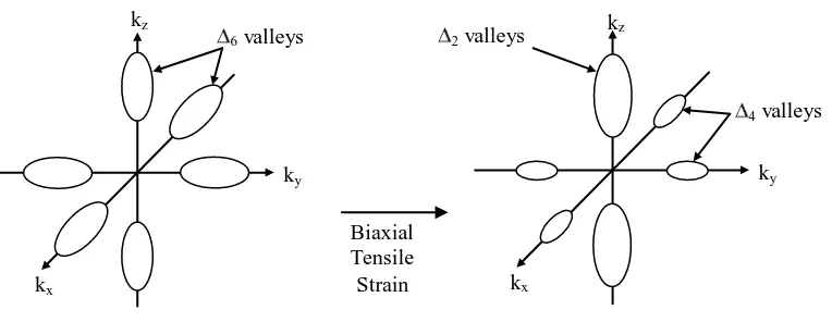
valence bands. The conduction band minima of unstrained silicon occur along the six
<001> crystal directions ( minima) and are six-fold degenerate. The application of
biaxial tensile strain lifts this degeneracy forming a two-fold and four-fold degenerate
set (Figure 1.3). The energy of the two-fold degenerate valleys are lowered,
becoming preferentially occupied by electrons, reducing intervalley scattering and
lowering the in-plane conduction mass (related to the curvature of the surface). This
yields a higher electron mobility (Rim et al. 2003) as can be seen from examination of
equation (1.2).
(1.2)
where q is electronic charge, is the mean free relaxation time of the carrier and m* is the carrier
[image:29.595.111.493.438.586.2]effective mass.
Figure 1.3 – Schematic representation of the constant-energy ellipses for unstrained and strained silicon showing the lifting of degeneracy by the application of tensile strain Takagi et al. (1996).
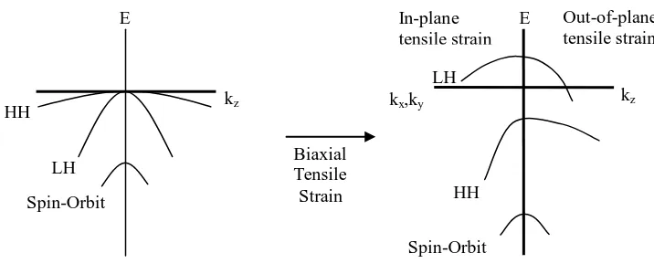
Similarly the valence band has degeneracy of the light and heavy hole bands
(so named because of the effective masses of carriers in these bands) lifted at the zone
centre (Figure 1.4). Greater strain is required to reduce inter-valley scattering in the Biaxial
Tensile Strain 6 valleys
kx
ky kz
2 valleys
4 valleys
kx
ky kz
*
valence band. For a recent review of the electrical properties of strained silicon the
[image:30.595.127.485.152.302.2]reader is referred to Nicholas (2004).
Figure 1.4 – Biaxial tensile induced changes in the valence band of silicon Rim et al. (2003).
The application of strain to silicon material within the channel region of an
FET (Field Effect Transistor) has been approached from two distinct directions.
Intel® has pioneered process-induced strain, where uniaxial strain (tensile or
compressive) is applied directly to the channel region of a device structure through
novel processing steps (Ghani et al. 2003). A second approach involves biaxial global
straining of the whole silicon layer. This is achieved through the epitaxial deposition
of a relaxed silicon-germanium layer possessing a greater lattice constant than bulk
silicon onto which a thin strained silicon channel may be deposited yielding a biaxial
tensile strained silicon layer. This global strain tuning layer is called a virtual
substrate, and the work in this thesis is concerned with investigations that could lead
to significant improvement in the quality of such structures. HH LH
Spin-Orbit In-plane tensile strain
Out-of-plane tensile strain
kz kx,ky
E
HH
LH
Spin-Orbit
kz E
1.4 Silicon-Germanium Technology
Incorporation of germanium into a silicon lattice can be achieved over the
entire compositional range of Si1-xGex for 0 < x < 1 to form a random alloy with the
lattice parameter varying almost linearly with composition, in close accordance with
Vegard’s Law (chapter 2 section 2.2.1). Interest in low composition relaxed virtual
substrates is mainly based on the benefits of increased carrier mobility provided,
whilst retaining compatibility with existing fabrication technology. Oberhüber et al.
(1998) have theoretically predicted enhancements for electron mobility in silicon,
when deposited on a fully relaxed Si1-xGex alloy with x = 15-25% to form a biaxial
tensile strained layer. An enhancement is also predicted for hole mobility but requires
a greater strain, equivalent of deposition on a fully relaxed silicon germanium alloy
with x = 30%. These predictions are shown graphically in Figure 1.5.
Figure 1.5 – Theoretical prediction of electron (dotted line) and hole (solid line) mobility enhancement in a strained silicon MOS device structure under low field conditions Oberhüber et al. (1998).
A major problem with this technology is that the quality of the virtual substrate is
compromised by defects generated by the strain relaxation process, leading to 2.6
2.4
2.2
2.0
1.8
1.6
1.4
1.2
1.0
0 10 20 30 40 50
M
obi
li
ty e
nha
nc
em
ent
f
ac
tor
Substrate Ge content [%] Holes
[image:31.595.172.407.420.610.2]degradation of device performance, reliability and yield issues and manufacturing
problems.
Germanium possess the highest bulk electron and hole mobilities of any bulk
elemental semiconductor (comparison with silicon given in Table 1.1) but the low
natural abundance of germanium makes bulk wafers uneconomic for mass production.
Bulk Electron Mobility (cm2V-1s-1)
Bulk Hole Mobility (cm2V-1s-1)
Silicon 1450 505
Germanium 3900 1800
Table 1.1 – Room temperature bulk lattice mobilities of electrons and holes in unstrained, undoped Si and Ge. Reproduced from a paper by Schäffler (1997).
The utilisation of silicon as a cheap platform on which a virtual substrate
based relaxed pure germanium structure is formed could allow the integration of III-V
optoelectronic devices, that share lattice parameters close to that of germanium (e.g.
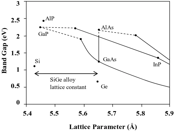
GaAs), to be incorporated into a highly integrated circuit, Figure 1.6.
Figure 1.6 – A map of band gap versus lattice constant for the III-V alloys and Si and Ge Fitzgerald et al. (1999).
3
2.5
2
1.5
1
0.5
0
5.4 5.5 5.6 5.7 5.8 5.9 SiGe alloy
lattice constant Si
Ge GaAs AlP
GaP
AlAs
InP
Lattice Parameter (Å)
Ba
n
d
G
a
p
(e
V
[image:32.595.106.489.223.304.2] [image:32.595.144.435.496.717.2]This would allow the development of optical interconnect technologies and allow
further assimilation of high frequency device architectures into highly integrated
circuits. Also the possibility of virtual substrate based germanium channel (relaxed or
strained) MOSFET devices is now of extreme interest with many investigations into
high-k dielectrics for germanium underway. This would allow very high channel
carrier mobilities to be harnessed and would provide a valuable performance boost to
the mainstream microelectronics industry.
1.5 Layer Transfer Technology
The reduction of transistor feature size has given rise to numerous so called
short channel effects (SCE) that become an increasing problem for smaller devices
(Nicholas 2004). To combat some of these effects AMD have introduced a layer
transfer technology into their mainstream device processing in the form of
silicon-on-insulator (SOI), demonstrating it to be a mature process (Soitec 2003). The SOI is
provided by bonding a thin (minimum 50 nm) silicon layer to the surface of an
oxidised silicon wafer forming an SOI structure, illustrated in Figure 1.7.
Figure 1.7 – Schematic illustration of the layered structure of an SOI (silicon-on-insulator) wafer.
The relevance of this technology in the current study is that the Smart Cut™
technology (Soitec 2003) used in the layer transfer process, can be equally applied to Silicon Substrate
Oxide Bonded Silicon Layer
the transfer of other materials, including a strained-silicon layer produced on a virtual
substrate. Critically this process removes the virtual substrate from the active layer.
In this situation the quality of the transferred layer reflects the quality of the virtual
substrate and is paramount, almost certainly impacting on the behaviour of the
strained layer during device processing. The possibility of re-growing and reusing the
base structure with this technology could further reduce cost.
1.6 Thesis Aims and Structure
The main drive of this thesis is to investigate and control the
silicon-germanium relaxation process to enable further improvement in the quality of relaxed
virtual structures. The virtual substrate structures were grown epitaxially using
solid-source MBE (molecular beam epitaxy) at the University of Warwick on commercial
silicon (001) orientated wafers. Specifically this work aims to extend that of
Capewell (2002) on a novel germanium grading technique, known as terrace grading,
to far greater thickness and composition ranges than hitherto, making comparison
with more conventional structures. Ultimately the work should enable progress
toward the production of planar, defect free platforms, terminating at an arbitrary
composition between silicon and pure germanium, thereby facilitating further
improvements in CMOS device performance and integration of III-V optical devices.
In the following chapters 2 and 3, the principles of silicon-germanium
epitaxial growth and strain relief along with a description of the experimental
techniques used in growth and characterisation are presented. In chapters 4, 5 and 6
experimental results and discussion for three compositional ranges are presented.
Chapter 7 summaries the key points of the investigation and draws conclusions based
Chapter 2
2
Principles of Epitaxial Growth and Strain Relief
In this chapter issues concerning the epitaxial growth of silicon and silicon
germanium alloys will be discussed and the process of strain relief through dislocation
formation and propagation introduced.
2.1 Epitaxial Growth
Epitaxial growth is the extension of a crystalline substrate in a planer manner.
A classical model of growth developed by Burton, Cabrera and Frank (BCF Model)
remains a useful starting point for our understanding of epitaxial crystal growth
(Burton et al. 1951). This classical work is not concerned with the reconstruction or
bonding of a real crystal surface and as such applies equally to all crystal systems.
Growth is described as a result of exchange of molecules between an adsorbed surface
layer and vapour (source of molecules) and diffusion of mobile species along the
surface until incorporated at a step edge or defect. Epitaxial growth can proceed with
the nucleation and growth of two dimensional islands (2-D island growth) by the
incorporation of mobile unbound surface atoms, now called adatoms, at the surface.
On a stepped surface growth can proceed by incorporation at the existing step edges
resulting in step flow growth. Recognition of the reality of imperfect surfaces is
highlighted as important in understanding nucleation rates observed in practice.
Knowledge of the movement of an adatom across a real silicon surface is
important in understanding epitaxial growth processes. The movement of an adatom
across an oxide free and clean silicon surface is greatly influenced by the
allows a reduction in the number of dangling bonds providing a lower surface energy
that is energetically favoured (Chadi 1983). A high temperature cleaned silicon (001)
surface has been found to display a (2x1) dimer construction lying along <110>
directions. A dimer is the rebonding of two neighbouring surface atoms due to the
re-hybridisation of the surface dangling bonds (Gawlinski and Gunton 1987).
The silicon substrates used for solid-source molecular beam epitaxy
(SS-MBE) in this work have vicinal surfaces (stepped) based on (001) with a surface
misorientation of around 0.1º toward <110>. Vicinal surfaces are preferred for
epitaxial growth because their stepped surface promotes layer-by-layer growth
through terrace extension (step flow) rather than 2-D islanding that can lead to less
perfect growth. Growth that proceeds primarily by 2-D island nucleation can lead to
the formation of anti-phase boundaries between separately nucleated islands, Figure
2.1.
Figure 2.1 – Schematic illustration of silicon islands on the Si (001) – (2x1) surface and the formation of antiphase domain boundaries when these islands intersect. Antiphase boundaries running parallel and perpendicular to the dimer rows are denoted AP1 and AP2 respectively. a0
is 3.85Å, the lattice (001) constant of the silicon (001) surface Bronikowski et al. (1993).
Anti-phase boundaries form because there are two possible sites at which islands can
nucleate; when islands initially formed from different sites meet they may be out of Growth
2a0 3a0
phase and unable coalesce, resulting in a row of surface vacancies and eventually
grown-in defects that may result in the loss of epitaxy (Bronikowski et al. 1993).
As growth proceeds the orientation of each subsequent layer is perpendicular
to the one before and a nomenclature related to the orientation of the dimerisation on
the top terrace to the step edge was proposed by Chadi (1987) (although the opposite
to that first proposed is now used!). A single step having an upper terrace with
dimerisation parallel to its edge is referred to as type A, SA, with the terrace above it
labelled TA, and a single step with upper terrace of dimerisation perpendicular to its
edge as a type B step, SB, terrace TB.
Figure 2.2 – Schematic representation of a vicinal silicon wafer surface. The mobile adatoms most easily move along dimer rows and this direction is indicated with arrows.
Figure 2.2 is a schematic representation of a vicinal silicon wafer surface.
Double height steps can also exist and are labelled DA and DB respectively as before
and are bounded by terraces of the same type. The reconstructed silicon surface
greatly influences adatom transport and it has experimentally been found that TA - Terrace
TA - Terrace TB - Terrace
SA - Step
SA - Step SB - Step
[image:37.595.104.496.327.587.2]transport along dimer rows occurs more rapidly than across them and was determined
by examination of denuded zone size (Mo and Lagally 1991). Due to the presence of
dangling bonds, attachment at the end of a dimer row is far more likely than at the
sides, for this reason TB terraces will generally advance more quickly than TA
terraces.
Jernigan and Thompson (2001) have investigated the evolution of a silicon
(001) substrate under normal growth temperatures (350 to 800ºC) and rates (1Å/s)
using Scanning Tunnelling Microscopy (STM) to directly image the surface. They
have shown that a transition from step flow to 2-D island growth occurred as the
temperature was reduced to around 500ºC and that the transition did not occur
abruptly, but for a limited temperature window showed characteristics of both growth
modes simultaneously. This transition marks a shift from growth dominated by
equilibrium processes to one more governed by kinetic processes. This transition will
be greatly dependent upon growth rate, surface orientation and the surface species
present.
2.2 Heteroepitaxial Growth
The growth of an atomic species upon a substrate of differing composition is
referred to as heteroepitaxy and is probably the most important application of epitaxy.
There are three recognised growth modes that can be adopted by heteroepitaxial
layers; the following inequality determines the mode of growth adopted:
(2.1)
where 12 - sum of the interface energy between the film and substrate, 1 - bare substrate surface 1
For lattice matched systems two dimensional Frank-van der Merwe (FvM) growth
will occur if equation (2.1) is satisfied (Frank and van der Merwe 1949). The epilayer
will otherwise be unable to wet the substrate surface and growth will result in the
formation of isolated three dimensional islands, Volmer-Weber growth (VW)
(Volmer and Weber 1926). For non-lattice matched systems strain plays an important
role in the evolution of film morphology. A strained epitaxial layer may initially
satisfy the above condition for Frank-van der Merwe growth, however at greater
thicknesses the strain energy of the film may be sufficient to negate this situation. If
such a situation occurs then growth will evolve from van der Merwe to the Volmer
Weber growth mode and as such is described separately as the Stranski-Krastanov
(SK) mode of growth (Stranski and Krastanov 1938). All 3 growth modes are
depicted in Figure 2.3. If the strained layer does not initially satisfy the condition in
equation (2.1) then growth is in the Volmer-Weber mode.
Figure 2.3 – Schematic representation of the growth modes (a) Frank-van der Merwe (FvM) (b) Volmer-Weber (VW) (c) Stranski-Krastanov (SK).
- Substrate
- Epitaxial Growth
(a) Frank-van der Merwe (FvM)
2.2.1 Germanium Incorporation
Silicon heteroepitaxy most commonly involves the addition of germanium and
is the main focus of the work presented herein. Germanium shares the same diamond
lattice structure as silicon having a bulk lattice constant (length of unit cell) ~4.2%
larger. The diamond lattice structure (Figure 2.4) consists of a face centred cubic
lattice (fcc) with a basis of atoms situated at (0, 0, 0) and (¼, ¼, ¼) relative to the
sides of the unit cell. Germanium forms a random alloy when introduced into a
silicon lattice (silicon and germanium atoms randomly occupy lattice sites) over the
entire compositional range, with the lattice parameter of the Si1-xGex mixture varying
almost linearly. This is in accordance with Vegard’s Law, an empirical rule that
predicts a linear relationship (at constant temperature) for the variation of lattice
constant for an alloy between that of the constituent elements. The epitaxial growth
of germanium and silicon-germanium alloy upon silicon has been found to follow a
Stranski-Krastanov growth mode where both growth rate and temperature are
important parameters.
Figure 2.4 – Schematic diagram of the silicon or germanium diamond crystal lattice. Lattice is fcc with a basis of atoms at (0, 0, 0) and (¼, ¼, ¼).
Position Markers


![Figure 2.10 – Diagram illustrating the relationship between dislocation Burgers vectors of the form ½[110], with specific reference to the (111) glide plane and its intersection with the (001) along the [-110] line direction](https://thumb-us.123doks.com/thumbv2/123dok_us/9784105.479503/51.595.108.508.439.679/diagram-illustrating-relationship-dislocation-burgers-reference-intersection-direction.webp)