Abstract—In this paper, we address a new PWM generation method and its hardware architecture for a large-size LED display system. Since the proposed probability-based PWM generator invokes pulses stochastically, the pulses can vary their positions even if the input PWM value is same. Furthermore, the periodic repeatability of PWM generation can be also removed, and thus the PWM pulses are evenly distributed in all time periods. The probability-based PWM method efficiently reduces the inrush current problem and maintains an image-quality without degradation. Experimental results using a commercial LED panel show that the proposed method is superior to previous ones in all aspects, such as the hardware cost, feasibility, and flexibility.
Index Terms— LED Display Controller, LFSR, Probability, PWM Dimming
I. INTRODUCTION
N LED has been going into new markets, such as mobile devices, lights, TV BLU(Back Light Unit), and traffic signs, due to many advantages in power consumption, brightness, life span, and viewing area. Since the rapid progress in an LED technology enables the high-quality full color images, the LED will be more popular and dominant essentials in display markets. In recent times, a large-size high-definition LED system displaying realistic images becomes a symbolic icon for high technology, and is widely used in stadium venues, outdoor billboards, and product showcases.
In order to generate high-quality images in large-size LED display, efficient LED controls of millions of LED components as well as the brightness and color gamut in each LED are key points. The brightness control methods in an LED output can be grouped roughly into two main categories: analog dimming and Pulse Width Modulation(PWM) dimming. An analog dimming is to control the LED current. As the brightness level in an LED is almost linearly proportional to the LED current, the desired brightness of the LED can be achieved by adjusting the current flow in a systematic way. The other one is a PWM dimming that switches the LED current on and off, and Manuscript received Dec. 08, 2010; revised Jan. 05, 2011. This work was supported by the Korean Ministry of Education, Science and Technology.
Authors marked with * are with the Electronic Engineering Department, Hoseo University, Asan, Chungnam, Korea (corresponding author to provide phone: +82-41-540-5667; fax: +82-41-540-5668; e-mail: jhahn@ hoseo.edu).
Authors marked with ** are with the EverBrighten Corporation, Asan, Chungnam, Korea (e-mail: [email protected]).
controls the average current. It is well-known that the PWM dimming is superior to analog method for implementing the high-quality video images in an LED display[1-2]. This is because the variation of the current amplitude causes the color gamut of an LED to deteriorate. Therefore, the constant current control of PWM can maintain the image color coherence in high-definition video images. However, previous PWM generation methods have some problems, such as an inrush current[2] and the heavy hardware cost. In this paper, we propose a probability-based PWM generation method and its hardware architecture for the large-size LED display system. The proposed method can solve aforementioned problems by probabilistic shifting PWM pulses with only several tens of logic gates and flip-flops.
II. RELATED WORKS
A. LED Display System
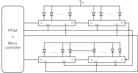
[image:1.595.313.549.608.732.2]A typical LED display system consists of a PC or video signal converter, a main controller, many LED module controllers, and a control software. First, a PC or video signal converter receives various video input signals, and then transmits corresponding video signals to the main controller. After dividing the input video image into the sub-images for the LED display module, the main controller distributes them to LED module controllers. Usually, the main controller also corrects the input images in terms of color enhancement, dot correction, brightness control, and so on. An LED module controller transmits the input sub-image to LED drivers by PWM and controls the module using common LED driving signals like CLK, ENABLE, and LATCH. The control software provides various image processing functions.
Fig. 1. Serial connection between a LED controller and LED drivers
An LED module control method depends on the connection form between an LED driver and a module
Probability-Based PWM Generator for
Large-Size LED Display System
Jin-Ho Ahn*, Sunghyun Park*, Kyoungwoon Son*, Minji Park*, Myungjib Moon*, Horyong Kim*, Eunae Hwang*, Woojoo Kim*, Uihwan Kim**, and Kwangyeon Kim**
controller. Generally, there are a parallel connection type, a serial type, a parallel-serial hybrid type, and a matrix type. Among them, for a large display system, the serial connection type has been widely used for reducing I/O pin overhead. In a serial mode, LED drivers are connected sequentially as shown in Figure 1. The number of LED driver ICs tied in a chain usually ranges from 64 to 256 considering the image refresh rate and the hardware redundancy.
B. PWM dimming for LED brightness control
The average power of PWM is linearly proportional to PWM pulse duration. Therefore, the control of pulse duration makes the same effect as one of the amount of LED current. In conventional linear PWM, however, no matter how PWM values are given, the PWM pulse is always invoked at the first cycle. Thus, it requires a large amount of current at the same time in the first cycle. This is called an inrush current[2]. The inrush current may induce several problems like the circuit malfunction due to Electro-Magnetic Interference(EMI)[3]. In order to solve those problems, several techniques capable of spreading the invoking pulses have been introduced. One of them is the Binary-weighted PWM(BPWM)[3]. BPWM gives different weights to each cycle and has an effect on the uniform distribution of PWM pulses. Another method is the Enhanced-Spectrum PWM (ES-PWM) implemented by Texas Instrument[4]. ES-PWM invokes pulses at regular intervals in such a way that pulses are generated at 1→ T/2→ T/4→ 3T/4→ T/8→ 5T/8→
3T/8→... in a zig-zag order(T means the one period of PWM). While ES-PWM is more efficient than linear PWM for the uniform distribution of PWM pulses, it is inferior to BPWM and the inrush current problem still remains. In addition, a sequential delayed-output of LED driving signals is utilized to reduce the inrush current problem[4]. But, it seems that accurate timing control is quite difficult and the hardware cost due to it may burden for the overall system implementation.
In summary, previous PWM generation techniques for the LED controller have common problems as follows:
(1) Conventional PWM generates pulses at the same position if the input value for PWM is identical. Therefore, as pixel values close by each other may be equal or similar in the high-definition image, the inrush current problem occurs frequently in serial connection mode of an LED display system.
(2) In general, the total number of PWM generator for a color LED module is Narray*3. Here, Narray denotes the number
of LED arrays in an LED module. Thus, in large-size LED display including tens or hundreds of LED modules, simple and efficient hardware architecture for PWM generation must be considered to increase the system productivity.
(3) Many LED driver IC makers have released various models from low-cost series[5] for affordable systems to high performance or multi-function series[6] for high-end systems. However, except for the LED current driving function, most of features influencing the image-quality like PWM resolution and dot correction[7] must be located in the LED module controller considering the maintenance and flexibility of the system.
III. PROBABILITY-BASED PWMGENERATION
A. Proposed PWM generation method
[image:2.595.305.547.296.380.2]An example is illustrated in Figure 2 to help the proposed ideas to be understandable. Figure 2 shows a timing diagram of 10-bit PWM. In this figure, one period(1024 clock cycle) includes 64-segment which size is 16. Two PWM signals having different duty cycles proportional to the input value are generated in a segment. One of both becomes the final PWM output by PWM select signal which is one of the segment control signals. In Figure 2, the duty cycle in PWM 1 is 1/16 and PWM 2 is 2/16, respectively. Let us assume that PWM 1(or PWM 2) is transmitted to the final PWM output if PWM select signal is low(or high). If the duty cycle of PWM select signal is 1/2, the final PWM signal corresponds to the PWM value, 96, according to the next calculation: 1024*((1/16)*(1/2)+(2/16)*(1/2)). The PWM resolution and the segment size can be chosen by considering the hardware size and randomness of PWM pulses.
Fig. 2. Basic concept of proposed PWM generation
B. Probability-based PWM generation with LFSR Linear-Feedback Shift Register(LFSR) is the shift register including a feedback path and is known as a pseudo-random pattern generator[8]. Since pseudo-random patterns occur algorithmically, all patterns except for all ‘0’ state are generated equally and the occurrence order repeats periodically. More details about LFSR refer to [8].
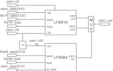
In Figure 3, the generic structure of probability-based 10-bit PWM generator using LFSRs is shown. The PWM generator consists of two main blocks that one is LFSR16 including a 4-bit LFSR and some combinational logics, and the other is LFSR64 composed of a 6-bit LFSR and a comparator. LFSR16 is a kind of weighted LFSR[9] and makes pwm_on1 and pwm_on2. LFSR64 produces pwm_sel signal. The I/O signal description is shown in Table 1.
Fig. 3. The structure of probability-based 10-bit PWM generator
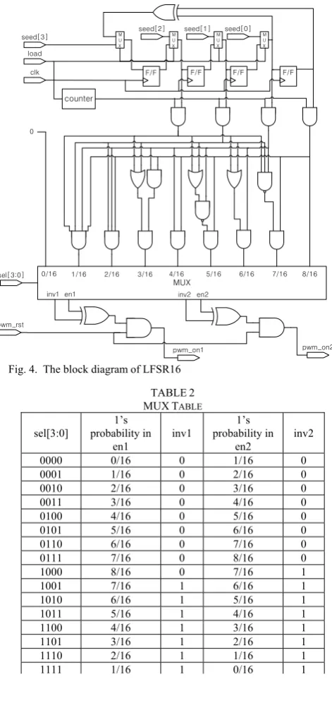
[image:2.595.308.547.602.753.2]The internal block diagram of LFSR16 is presented in Figure 4. Characteristic polynomial p(x) of 4-bit LFSR in the figure is x4+x+1 and satisfies the maximal-length
condition[8]. So, the LFSR will produce the number from 1 to 15 randomly. The frequency of ‘0’ and ‘1’ at LFSR F/F outputs can be controlled by a combinational logic tree and this is called the weighted LFSR[9]. To let the occurrence frequency of ‘0’ and ‘1’ be the same in all F/F outputs, the LFSR must generate the patterns from 0 to 15 only once within a period. However, as normal LFSR cannot produce the all ‘0’ state, we set the state on purpose. For example, on the assumption that the seed is (1 0 0 0), 4bit LFSR in Figure 4 will produce the patterns as the following order: (1 0 0 0) → (0 1 0 0) → (0 0 1 0) → ... → (0 0 1 1) → (0 0 0 1) → (1 0 0 0)... At this time, if we change the repeated value, (1 0 0 0) into (0 0 0 0), all values from 0 to 15 can be obtained. We use a counter to check the repeated one in the proposed architecture. Though the procedure to configure the all ‘0’ state deteriorates the randomness of patterns slightly, this method has the advantages of making the occurrence frequency of ‘0’ and ‘1’ to be equal without disturbing LFSR operations, and changing LFSR seed automatically to remove the periodic repetition. In the figure, we can simply estimate that the first seed value, (1 0 0 0), goes to (0 1 0 0) in the next period.
Now, we address the probability control of ‘1’ indicating the PWM pulse. In Figure 4, the probability of ‘1’ at the rightmost F/F output in the LFSR is 1/2(=8/16 in the figure). If the two signals which the probability of ‘1’ is 1/2 enter an AND gate, the probability of ‘1’ of AND gate output will be 1/4(=4/16). We can also obtain 1/8(AND gating between 1/2 and 1/4), 3/4(OR gating both 1/2 signals), 3/8(AND gating between 1/2 and 3/4), and so on. After repeating the same procedure, 9 probability values are acquired as follows: 0/16, 1/16, 2/16, 3/16, 4/16, 5/16, 6/16, 7/16, 8/16. These probability values can be converted to other values from 9/16 to 16/16 using an XOR gate. For example, XOR gating between a signal having ‘1’ at the rate of 3/16 and a signal having always ‘1’ results in 13/16. As we can see in the figure, the inv signals have a role of XOR gate control. According to the input PWM value, two PWM signals, pwm_on1 and pwm_on2, representing different duty cycles are produced in LFSR16. Upper 4-bit data(=sel) among 10-bit PWM value(pwm_data) is utilized to select one of input probability
values and determines whether it alters via the inv signal. The MUX table on the basis of sel signal is shown in Table 1. For reference, the combinational logic tree in Figure 4 is not optimized to understand the proposed structure easily and will be shrunk considerably by the logic optimization process. In addition, LFSR16 can change the seed value in a user mode. While the parallel structure for loading seed is implemented in Figure 4, we can simply modify it to a serial loading type for diminishing the hardware cost if timing space is given.
pwm_rst clk
MUX
0/16 1/16 2/16 3/16 4/16 5/16 6/16 7/16 8/16
F/F F/F F/F F/F
[image:3.595.46.289.54.237.2]sel[3:0] inv1 en1 pwm_on1 seed[3] load M U X M U X seed[2] M U X seed[1] M U X seed[0] inv2 en2 pwm_on2 0 counter
Fig. 4. The block diagram of LFSR16
- Detail operations in LFSR64 block
The overall structure of LFSR64 is shown in Figure 5. The basic operation of LFSR64 is almost the same as LFSR16. A 6-bit LFSR in LFSR64 generates the numbers from 1 to 63 randomly and we modify the range from 0 to 63 using a counter. Modified pseudo-random pattern sequence (=cmp_data) is compared to lower 6-bit data of pwm_data (=ref_data), and then creates the pwm_sel signal in the TABLE1
I/O SIGNAL DESCRIPTION
Name Type Size Function pwm_clk input 1 PWM operation clock
pwm_data input 10
PWM value. Upper 4bit data is used for LFSR16 and lower 6bit is used for LFSR64
lfsr16_see
d input 4 4-bit LFSR seed for LFSR16 lfsr16_load input 1 lfsr16_seed loading signal. Active
high
pwm_rst input 1 PWM initialization signal. Active low
lfsr64_see
d input 6 6-bit LFSR seed for LFSR64
lfsr64_load input 1 lfsr64_seed loading signal. Active high
pwm_out output 1 Final PWM signal for pwm_data. Active high
TABLE2 MUXTABLE
sel[3:0] 1’s probability in en1 inv1 1’s probability in en2 inv2
0000 0/16 0 1/16 0 0001 1/16 0 2/16 0 0010 2/16 0 3/16 0 0011 3/16 0 4/16 0 0100 4/16 0 5/16 0 0101 5/16 0 6/16 0 0110 6/16 0 7/16 0 0111 7/16 0 8/16 0 1000 8/16 0 7/16 1 1001 7/16 1 6/16 1 1010 6/16 1 5/16 1 1011 5/16 1 4/16 1 1100 4/16 1 3/16 1 1101 3/16 1 2/16 1 1110 2/16 1 1/16 1
[image:3.595.309.545.183.682.2]following way:
if(ref_data > ~cmp_data) pwm_sel = 1; (pwm_on2 is chosen) else pwm_sel = 0; (pwm_on1 is chosen)
[image:4.595.303.557.125.202.2]The operation clock frequency of LFSR64 should be one sixteen of one of LFSR16, because pwm_sel varies by the segment.
Fig. 5. The block diagram of LFSR64
IV. IMPLEMENTATION RESULTS
A. HDL simulation
Firstly, the proposed probability-based PWM generator was designed by verilog-HDL and simulated on the ModelSim -Altera v.6.5e from Mento Graphics. Figure 6 displays the simulation result of LFSR16.
Fig. 6. The simulation result of LFSR16
In the figure, when input PWM value is 0111011111b (479d) and the seed value is 1000b, lfsr_ff indicates the LFSR outputs during the one period of LFSR. The first
[image:4.595.48.278.147.277.2]pattern, 10d, of lfsr_ff is initialized by a counter, and then the new pattern sequence(=gff) is produced. Next, the gff values enter MUX via a combinational logic tree. According to the MUX table in Table 2, pwm_on1 will be invoked at the rate of 7/16 and pwm_on2 will be invoked at 8/16 as sel is 0111b.
Fig. 7. The simulation result of LFSR64
The simulation result of LFSR64 is presented in Figure 7. As mentioned in chapter 3, in case that cmp_data is greater than ref_data, pwm_on2 will be the final PWM output (=pwm_out) due to activated pwm_sel signal. At the other case, pwm_on1 will be so. In order to remove the critical timing problem, the pwm_out for LED drivers is latched by F/F. This is reason for some delay shown in the figure.
B. Board-level implementation
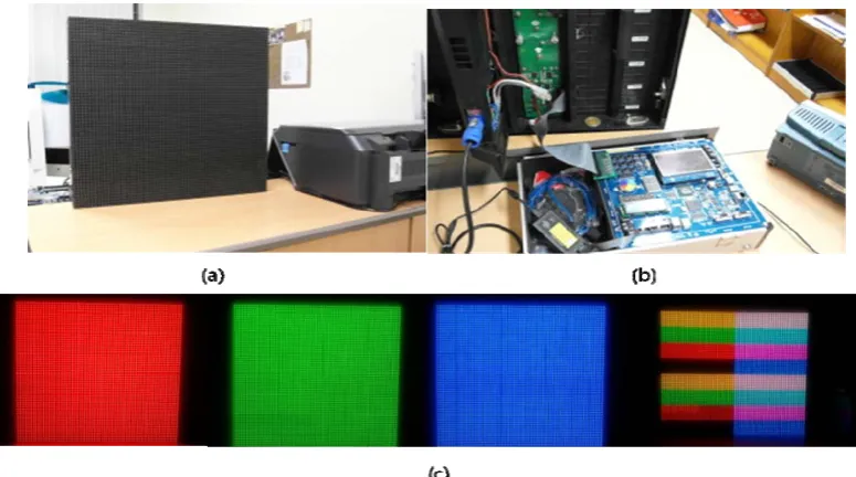
After doing functional verification, we tried a board-level implementation using an FPGA system adopting Cyclone II model of Altera and a commercial LED module produced by EverBrighten company[10]. As a result of implementation, the proposed PWM generator could be realized with 45 gates and 41 registers in terms of hardware size. This is only about 0.1% of logic elements in Cyclone II. For reference, we set the clock frequency(=pwm_clk) to 25MHz and the refresh rate of output image to 95Hz. Figure 8 (a) is the LED display module used in the experiments and (b) is the connecting state between LED module and FPGA system. The various color representation results using the proposed method are illustrated in Figure 8 (c). We next observed the image-quality and confirmed that the brightness of image was comparable to commercial products and degradation due to blots and juddering didn’t appear.
[image:4.595.47.296.410.479.2] [image:4.595.101.489.553.769.2]V. CONCLUSION
In this paper, we propose a probability-based PWM generation method and its hardware architecture suitable for a large-size LED display system. The proposed method can efficiently solve problems of previous PWM dimming-based LED display by probabilistic shifting of PWM pulses only with several tens of logic gates and flip-flops. Experimental results on a commercial LED panel show that the proposed idea satisfies the image quality, operation speed, hardware cost, and other requirements for a LED module controller.
REFERENCES
[1] M. Day, “LED Dimming Techniques Enhance Video Display Image Quality,” LED Journal, April, 2010
[2] M. Day and T. Saab, “TLC5940 dot correction compensates for variations in LED brightness,” Analog Applications Journal, 2005 [3] L. Svilainis, “LED brightness control for video display application,”
Displays, Vol. 29, pp, 506-511, 2008
[4] Texas Instrument, TLC5943 Data Sheet, Dec. 2007
[5] Silicon Touch Technology Inc., DM13H Data Sheet, Feb. 2010 [6] STMicroelectronics, STP24DP05 Data Sheet, Nov. 2009
[7] M. Day, “TLC5940 PWM dimming provides superior color quality in LED video displays,” Analog Applications Journal, 2006
[8] P. H. Bardell et al., “Built-In Test for VLSI: Pseudorandom Techniques,” John Wiley & Sons, Somerset, NJ, 1987
[9] M. Bushnell and V. Agrawal, “Essentials of Electronic Testing for Digital, Memory, and Mixed-Signal VLSI Circuits,” Kluwer Academic Publishers, 2000