474 |
P a g e
REDUCTION OF HARMONICS CAUSED DUE TO
SMPS USING SIGMA DELTA MODULATION
1
Ms.Madhuri U Naik,
2Prof .A. A. Apte
1,2
All India Shree Shivaji Memorial Society’s College of Engineering, Pune (India)
ABSTRACT
The harmonic currents generated by the modern power supply equipment cause power system heating and also add to user power bills. Personal computers are the major equipments which use the modern power supply ie switched mode power supply (SMPS).These SMPS draw non-sinusoidal currents from the supply which results in generation of harmonics. Power quality of the distribution network is been disturbed by these harmonics during the operation of the electronic load. The switching currents can cause electrical noise problems if not carefully suppressed, and simple designs may have a poor power factor. This paper presents a new method, sigma delta modulation to control the SMPS operation and minimise the harmonics generated by it.
Keywords—
Harmonics, Power Supply, Power Quality, Switch Mode Power Supply
I. INTRODUCTION
Switch-mode power supplies (SMPS) are a popular and sometimes necessary choice for DC-DC power
conversion. These circuits offer distinct benefits and tradeoffs when compared to alternative methods of
converting DC power. A switched-mode power supply is an electronic power supply that incorporates a
switching regulator to convert electrical power efficiently. Like other power supplies, an SMPS transfers power
from a source, like mains power, to a load, such as a personal computer, while converting voltage and current
characteristics. Unlike a linear power supply, the MOSFET of a SMPS continually switches between
low-dissipation, full-on and full-off states, and spends very little time in the high dissipation transitions, which
minimizes wasted energy. Ideally, a SMPS dissipates no power. Voltage regulation is achieved by varying the
ratio of on-to-off time. In contrast, a linear power supply regulates the output voltage by continually dissipating
power in the pass MOSFET.[1] This higher power conversion efficiency is an important advantage of a SMPS.
This switching action of SMPS changes the characteristics of input current which leads to current harmonics.[2]
The objective of this paper is to minimize these harmonics by using proper control. SMPS are used where higher
efficiency, smaller size and lighter weight are required.
II. WORKING OF SWITCH MODE POWER SUPPLY
475 |
P a g e
In an SMPS, ac supply is first rectified, and then filtered by the input reservoir capacitor to produce a
rough dc input supply. This level can fluctuate widely due to variations in the mains. In addition the capacitance
on the input has to be fairly large to hold up the supply in case of a severe drop in the mains. (The SMPS can
also be configured to operate from any suitable dc input, in this case the supply is called a dc to dc converter.)
The unregulated dc is fed directly to the central block of the supply, the high frequency power switching section.
Fast switching power semiconductor devices such as MOSFETs are driven on and off, and switch the input
voltage across the primary of the power transformer. The drive pulses are normally fixed frequency (20 to 200
kHz) and variable duty cycle. Hence, a voltage pulse train of suitable magnitude and duty ratio appears on the
transformer secondary. This voltage pulse train is appropriately rectified, and then smoothed by the output filter,
which is either a capacitor or capacitor/inductor arrangement, depending upon the topology used.[3] This
transfer of power has to be carried out with the lowest losses possible, to maintain efficiency. Thus, optimum
design of the passive and magnetic components, and selection of the correct power semiconductors is critical.
Regulation of the output to provide a stabilized dc supply is carried out by the control feedback block.
Generally, most SMPS systems operate on a fixed frequency pulse width modulation basis, where the duration
of the on time of the drive to the power switch is varied on a cycle by cycle basis. This compensates for changes
in the input supply and output load.[4] The output voltage is compared to an accurate reference supply, and the
error voltage produced by the comparator is used by dedicated control logic to terminate the drive pulse to the
main power switch/switches at the correct instance. Correctly designed, this will provide a very stable dc output
supply.
In most applications, the SMPS topology contains a power transformer. This provides isolation, voltage
scaling through the turns ratio, and the ability to provide multiple outputs.[6] However, there are non-isolated
topologies (without transformers) such as the buck and the boost converters, where the power processing is
achieved by inductive energy transfer alone.
A. Delta Modulation (DM) Scheme
DM is basically an analog to digital conversion process. In DM the difference between samples is encoded
into binary symbols.
Fig1.2: Block diagram for Delta Modulator
476 |
P a g e
e(t)= Quantization error
m(t)= integrated output of previous sample
In DM rather than quantizing (approximation) the absolute value of the input analog waveform, DM quantizes
the difference between the current and the previous step, as shown in the Fig 1.2. The modulator is made by a
quantizer which converts the difference between the input signal and the average of the previous steps. In its
simplest form, the quantizer can be realized with a comparator referenced to 0 (two levels quantizer), whose
output is 1 or 0 if the input signal is positive or negative.[7] If the sampling interval „Ts‟ in Digital Pulse Code
Modulation (DPCM) is reduced considerably, i.e. if we sample a band limited signal at a rate much faster than the
nyquist sampling rate, the adjacent samples should have higher correlation. The sample-to-sample amplitude
difference will usually be very small.
B. Adaptive Delta Modulation Scheme
ADM modulator is the modification of delta modulator.[9] In delta modulation the step size is constant while in
adaptive delta modulation the step size varies according to the amplitude of input signal, ie it has controllable step
size as shown in fig 1.3 - the control being sensitive to the slope of the sampled signal.
Fig1.3: Block diagram for Adaptive Delta Modulator
C. Sigma Delta Modulation Scheme
The work on sigma-delta modulation (SDM) was developed as an extension to the well established DM. The
design of sigma-delta (SD)(Δ∑) analog-to digital converters (ADCs) is approximately three-quarters digital and
one-quarter analog. SD ADCs are now ideal for converting analog signals over a wide range of frequencies, from
DC to several megahertz.[10]Basically, these converters consist of an oversampling modulator followed by a
digital/ decimation filter that together produce a high-resolution data-stream output.
477 |
P a g e
fs = Sampling Frequency
ei = Quantization error
In an SMPS the input sinusoidal voltage is first rectified and then this rectified voltage is given as an input to the
different control circuits as explained above, where the rectified analog voltage signal is converted to digital.[11]
And this digital pulses are given as switching signal to the switch of boost converter as shown in the fig 1.5.
Fig1.5: SMPS with control scheme
III. HARDWARE MODEL WITH SIGMA DELTA AS CONTROL CIRCUIT
478 |
P a g e
Fig 2.2: Input current and voltage waveform Fig2.3: Frequency spectrum of input current.
The above figure shows the hardware model of an SMPS with sigma delta(SD) control. Here we are using an
step down transformer to reduce the 230V to 15V. As seen in fig there are two transformers, out of which one is
used to give supply to the main rectifier of SMPS and the other transformer is used to give supply to the control
circuit rectifier. Since the input to the SD control is the rectified voltage, this is an separate rectifier build for
control circuit.[14] The rectified voltage from the main rectifier is given to the boost converter where the value of
L is designed to 3.75mH depending on the input voltage and duty cycle. The SD control is designed in the form
of an code written in the PIC16F873 microcontroller. It is an single chip ,28 pins microcontroller that contains the
processor (the CPU), non-volatile memory for the program (ROM or flash), volatile memory for input and output
(RAM), a clock and an I/O control unit. Fig 2.2 shows the frequency spectrum of the input current for the
hardware model. It is clear from the figure that the frequencies of higher order goes on decreasing
IV. RESULTS
Simulation Results
479 |
P a g e
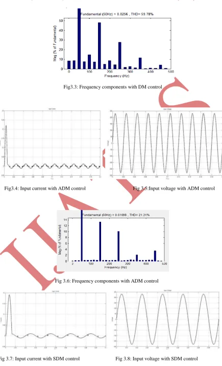
Fig3.3: Frequency components with DM control
Fig3.4: Input current with ADM control Fig 3.5:Input voltage with ADM control
Fig 3.6: Frequency components with ADM control
480 |
P a g e
Fig3.9: Frequency components with SDM control
V CONCLUSION
The current waveform with different control schemes is shown for matlab simulation and hardware model.
Frequency component for simulation results are shown in the form of bar graph which concludes that the 3rd
order harmonic components appear to be minimum in SDM control. The FFT analysis of the current waveform
for hardware is shown in fig 2 which shows that the higher order harmonics reduce down in magnitude. Hence
SDM control scheme has reduced Total Harmonic Distortion (THD) compared with the DM and ADM scheme.
SDM control scheme operates with a very high frequency than DM and ADM, which helps in following the
rectified voltage waveform more accurately ie it follows the input signal and helps in reducing harmonics.
Hence the switch operated with SD gives more sinusoidal current and reduced THD
REFERENCE
[1] Qihong Huang „Harmonic reduction in a single switch three phase boost rectifier with harmonic injected PWM‟,Thesis submitted to the Faculty of The Virginia Polytechnic Institute and State University in partial
fulfillment of the requirements for the degree Master of Science in Eletrical Engineering
[2] Mariusz Malinowski, „Sensorless Control Strategies for Three - Phase PWM Rectifiers‟ Ph.D. Thesis M. Sc
Warsaw University of Technology Faculty of Electrical Engineering Institute of Control and Industrial
Electronics. Warsaw, Poland – 2001.
[3] Amit Kumar Jain, Engineering Technical Staff, Analog Power Design Inc, Raja Ayyanar, Associate
Professor, Department of Electrical Engineering, Arizona State University ,Section 22,‟Power Electronics‟
[4] Thomas Key, Jih Sheng lai , „Cost and benefits of harmonic current reduction for switched mode power
supply‟,IEEE 1100 Power Electronics application center, Knoxvilley, Oak Ridge National Laboratory,
Tennessee.
[5] António P. Martins‟The Use of an Active Power Filter for Harmonic Elimination and Power Quality Improvement in a Nonlinear Loaded Electrical Installation‟ Institute of Systems and Robotics –
Porto,Faculty of
Engineering – University of Porto.
[6] A.N.Malleswara Rao, Dr. K. Ramesh Reddy,Dr. B.V.Sanker Ram / International Journal of Engineering
481 |
P a g e
[7] M. Davari, B. Abdi, Nafisi „State Feedback Control of Boost Converter UsingS1- Δ∑ PWM Method „,2nd
IEEE International Conference on Power and Energy (PECon 08), December 1-3, 2008, Johor Baharu,
Malaysia
[8] Siew-Chong Tan, Student Member, Y. M. Lai, Student Member, Chi K. Tse, Senior Member, IEEE, Martin
K.H. Cheung, Student Member „A Fixed-Frequency Pulsewidth Modulation Based Quasi-Sliding-Mode
Controller for Buck Converters
[9] Clemens M. Zierhofer, „Adaptive Sigma–Delta Modulation With One-Bit Quantization‟, IEEE Transaction
on circuits and systems-II: Analog And Digital Processing,Vol.47,No 5,May 2000.
[10] Jeyanandh Paramesh, Annette von Jouanne, „Use of Sigma–Delta Modulation to Control EMI from Switch-
Mode Power Supplies‟ Senior Member, IEEE, IEEE Transactions on Industrial Electronics, Vol.48, No.1,
February 2001
[11] C.H.Bae, K.B.Lee and K.W.Lee „Sinusoidalisation of the input curent in boost-type rectifier using sigma
delta modulation schemes‟ ,IEEE Proc.-Electr. Power Appl., Vol.151, No. 6 November 2004.
[12] Antunes, V.M.E.; Pires, V.F.; Silva, J.F. Digital multilevel audio power amplifier with a MASH sigma-delta
modulator to reduce harmonic distortion. Industrial Electronics, 2005. ISIE 2005. Proceedings of the IEEE
International Symposium on, Vol. 2:525–528, June 2005.
[13] Gray, Robert M. Spectral Analysis of Quantization Noise in a Single- Loop Sigma-Delta Modulator with dc
Input. IEEE Transactions on Communications, Vol. 37(6):588–599, 1989.
[14] J.G. Proakis and D.G. Manolakis, “Digital Signal Processing,” Fourth edition, Prentice Hall of India Private