FPGA BASED EXPLOSION ANALYZER
Swati M Patil
Department of Electronics & Telecommunication Engineering, S. J. C.E.T. Palghar, (India)
ABSTRACT
The proposed Explosion Analyzer is a portable device that monitors the fragments and air shock waves emitted
by any explosive device. The digital signals are stored in a memory. The stored data can be used for further
analysis. This device can be used in remote areas where human interference is not possible. The Explosion
Analyzer fills the void between expensive analyzers with many channels, and inexpensive analyzers with few
channels and limited sample rates. The design of the EA presented in this paper can be effectively used in
remote areas. It has 32 channels and can login a large amount of data of 80MB in time period of 1 second. It is
also having very high sampling rate of 20M samples/sec of width 32 bits. It is also interfaced with PC. After
explosion test the data can be transferred to PC and displayed in graphical format and can be further analyzed.
It uses FPGA for high speed data acquisition and stores in PSRAM. It also uses a micro controller (AVR) for
transferring the test data into SD card and later transferring it to PC via serial interface.
Keywords: Explosion Analyzer, Field Programmable Gate Array, Liquid Crystal Diode, Personal
Computer, Pseudo Static Random Access Memory
I.INTRODUCTION
1.1. Goals
The proposed digital Explosion analyzer is used to measure the intensity of mechanical wave in a time period
of 1 second with a sampling rate of 50 nanosecond. In this logging period we are logging data of 80 MB. (32
bit*20MHz = 80M samples/sec).
The instrument must be portable and have battery backup. It must have storage capacity of at least 10 tests in
non volatile memory. Also it should have the capability to interface with PC via serial communication.
1.2 System Discription
In this project Explosion analyzer (EA), there are two main parts and we require two main platforms which are
FPGA for data logging portion and Micro-controller (AVR) for co-ordination and communication with PC or
backup memory. In data login part the two main hard wares interfaced are FPGA and external PSRAM and in micro-controller portion, the controller used is AVR for storing large data and it is also interfaced with RTC,
keyboard, LCD, SD card, PC for viewing the result in graphical format. This LSA starts recording the data when
it receives any start input pulse. Switches are used as sensors. When any mechanical wave or
II. BLOCK DIAGRAM OF PROPOSED EA
Fig 1 shows Explosion analyzer is used to measure the intensity of air shock wave in a time period of 1 second
keyboard, RTC, PC and memory. Initially after power on FPGA is in reset state. A menu will be displayed on
LCD like login mode, test mode, RTC, view data from PC, Retrieve data.
When login mode is selected micro controller releases FPGA. After this if FPGA receives any input signal then
it starts login the data. When the logic state changes the FPGA stops login the data. FPGA stores this data in
PSRAM. FPGA reads the data from memory and sends 1 byte data to the micro controller with each clock pulse.
Fig.1 Block Diagram of Proposed EA
The micro controller stores the data in SD card. If test mode is selected then FPGA will be self tested. If RTC
option is chosen then we can set the time and date of received data. We can view the data in graphical format
from PC if we choose the view data from PC option. If retrieve data option is chosen then micro controller reads
the stored data from memory.
III. THE DATA AQUISATION PORTION (FPGA & PSRAM)
In data aquisation , two hardware’s used that are field programmable gate array (FPGA) of Altera Cyclone II
and Pseudo Static Random access memory (PSRAM) which is of 80 Megabytes in sized. Language used for
coding of data login portion is verilog hard ware description language. For simulation of data login portion,
Modelsim platform is used and for synthesis Quartus II 10.1 web edition platform is used.
3.1. PSRAM (Pseudo Static Random Access Memory)
PSRAM is a dynamic RAM with built-in refresh mechanism and address-control. It is behave similarly to static RAM (SRAM). It combines the high density of DRAM with the ease of use of SRAM. Pseudo Static RAM
typically features high speed, density and inexpensive cost structure. The access time of PSRAM is 70 ns and
DPD current is 10µA. It has UB/LB byte control and wide operating temperature range is –30 to +85°C.
PSRAM also has low power features which are Deep Power-Down (DPD) refresh mechanism, Partial Array
Refresh (PAR) mechanism and Temperature Compensated Refresh (TCR) mechanism [4].
3.2. FPGA CHIP of Altera Cyclone II
Field Programmable means that the FPGA's function is defined by a user's program rather than by the
manufacturer of the device. A small device may be present to allow the designers to change a board's glue logic
more easily during product development and testing. There are various types FPGA Manufactures such as
Xilinx, Altera and Lattice etc. From these manufactures, here we used Altera family which has very low cost, fast interfaces to external RAM. It is Seven member family offers densities ranging from 4000 to 68416 logic
elements. It provides clock rates up to 260 MHz[5].
IV. INTERNAL BLOCK DIAGRAM OF PROPOSED EXPLOSIVE ANALYZER
Fig2 Internal Design of Proposed EA
Fig 2 shows the architecture of Explosion Analyzer in which we have used Asynchronous start pulse. There are
two D type flip-flops, one is asynchronous and other is synchronous The asynchronous D type flip-flop is used
to receive this start pulse. To make this start pulse synchronize with clock the second D type flip-flop is used.
Due to this the writing pulse will get sufficient time to write data in memory.
The output of synchronize D type flip-flop is acting as a read signal, ready signal and also acting as a control signal of tri-state buffer. When this control signal becomes one, the data on the input line of tri-state buffer
transfers to the data line of the memory. The output of D type flip-flop also acts as an input of AND gate that’s another input is a clock from oscillator. The output of AND gate is acting as an input of OR gate who’s another
input is a clock from micro-controller. The output of OR gate is acting as a clock to the counter and another
input of counter is reset which is an output of OR gate. The inputs of OR gate are external reset and reset signal
from micro-controller. This counter is design for updating the memory location.
In this Explosion Analyzer, I have designed internal oscillator to get the 20 MHz clock frequency. This
50 nsec. Due to this the memory couldn’t get the enough time to perform writing and reading operation. So
making of two banks of memory is necessary.
During write operation, in the first bank of memory the data is directly written and in the second bank of
memory the data is written through latch i.e. in first 50 nsec. data is stored in latch and in next 50 nsec. the data
is stored in memory. Due to this the memory will get sufficient time for writing data into the memory. So that during writing operation first lower bank is selected and then upper bank is selected.
During reading operation, bank is selected using bank_select signal from micro-controller. This bank_select
signal is ANDing with not of RUN signal. When this signal become one then the data from lower bank of
memory is read and goes towards multiplexer and then to the micro-controller. When bank_select signal goes
low, upper bank of memory is selected, data from upper bank of memory is read and goes towards multiplexer
and to the micro-controller.
4.1 Timing Diagram
V. THE MICRO-CONTROLLER SECTION FOR USER INTERFACE
The hard wares used in microcontroller section are 8-bit Micro-controller (AVR 128), Serial flash memory (80
MB), LCD, Keyboard, RTC and PC. Language used for coding purposed are Embedded C and VC++. Platforms
used for microcontroller are AVR Studio 4.0, Microsoft visual studio 6.0(for serial communication)
5.1 Advantages of Atmel Avr
The very lowest-price microcontroller available from any manufacturer is the $0.54 Atmel AVR ATtiny11 6
MHz FLASH (same price for 8 pin DIP and 8 pin SOIC). Speed: Not only are most AVR capable of 20MHz (even really cheap ones like the ATtiny25/45/85 and ATmega48), but they actually run at near 20 MIPS; the
PIC chips of higher price (for example, PIC16F88) only run at 5 MHz with a 20 MHz oscillator frequency. In
addition, with the better addressing modes and registers of the AVR, most operation can be done in only one
instruction, where it often takes more than one instruction to do the same thing on a PIC. One big advantage of
AVRs is that they are supported by the GNU Compiler Collection (GCC). AVR 128 is a High-performance,
Low-power AVR 8-bit Microcontroller. It has Advanced RISC Architecture i.e. 133 Powerful Instructions Most
Single Clock Cycle Execution, 32 x 8 General Purpose Working Registers + Peripheral Control Registers, High
Endurance Non-volatile Memory segments i.e. 128K Bytes of In-System Self-programmable Flash program
I/O and Packages are 53 Programmable I/O Lines and 64-lead TQFP and 64-pad QFN/MLF. AVR
microcontroller Operating Voltages are 2.7 - 5.5V for ATmega128L and 4.5 - 5.5V for ATmega128. It has
Speed Grades of 0 - 8 MHz for ATmega128L and 0 - 16 MHz for Atmega12
5.2 Sd Card (1 GB)
Secure Digital (SD) is a flash (non-volatile) memory card format developed for use in portable devices. SD card capacities range from 8 MB to 16 GB.[10]
5.3. RTC
A real-time clock (RTC) is a clock that keeps track of the current time. In this DS1307 serial real-time clock
(RTC) is used. It is a low-power, full binary-coded decimal (BCD) clock/calendar, 56 bytes of NV SRAM,
address and data are transferred serially through an I²C, bi-directional bus, Operating voltage 5 V, operating
frequency is 32.768k Hz and optional Industrial Temperature Range -40°C to +85°C[8].
5.4 User Interface
Serial communication is used for the purpose of data transferring between micro-controller and PC and the data
can be read from PC in graphical format.
VI. SIMULATION RESULTS
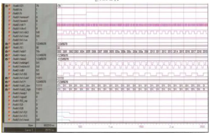
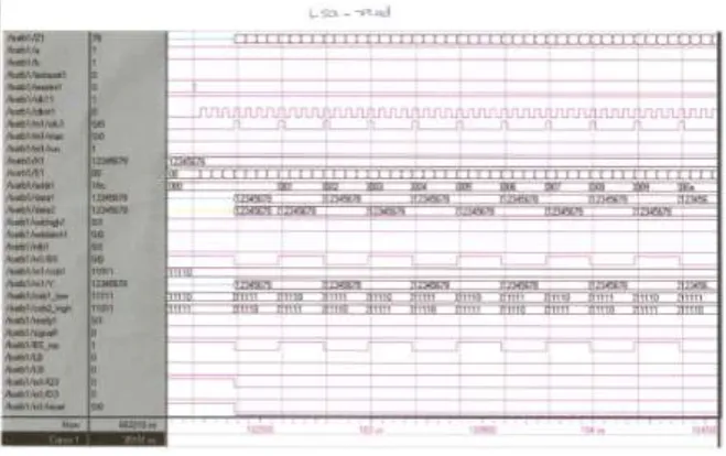
Fig 3 shows the data acquisition process through FPGA and saved in memory. After FPGA give ready signal to
microcontroller for receiving clock pulse from microcontroller which is slower in speed than data acquisition
rate and in fig 4 FPGA received clock from microcontroller FPGA give 8 bit data to microcontroller for further
analysis
Fig 4 Data Retrieved from Memory
VII. CONCLUSION
The Explosion Analyzer has been designed for specific use like vibration & explosive studies i.e. this EA is used
for measuring the strength or velocity of fragments and there by measuring the explosive power of the explosive device i.e.
80 Mega samples / sec. This Explosion Analyzer also meets the portability for acquiring large data and also has battery
backup.
REFERENCE
[1] Article Sources and Contributors Logic analyzer Source: http://en.wikipedia.org/
w/index.php?oldid=382892919
[2] “Logic Analyzer manual version 1.00” issued by Guangzhou ZHIYUAN electronics co. Pvt Ltd. [3] Primer, “The XYZs of Logic Analyzer”, accessed from http:// www.tektronix.com /
[4] Micron Technology, “ (MT45W4MW16PCGA) PSRAM data sheet”
[5]Documentation on the FPGA, programming model and software modules from Altera:
http://www.altera.com/literature
[6] Samir Palnitkar, “Verilog HDL- A guide to Digital Design and Synthesis”, SunSoft [7] Kanatkar “ Let Us C”
[8] AVR 128 data sheet
[9] RTC DS 1307 data sheet
[10] Keyboard IC MM74C923 datasheet
[11] www.google.com
[12] Article Sources and Contributors Logic analyzer Source: http://en.wikipedia.org/
w/index.php?oldid=382892919
[13] http://en.wikipedia.org/wiki/Logic_analyzer [14] Hyundai “HY62256A SRAM datasheet “