PHASE CHANGE MEMORY: ARRAY DEVELOPMENT AND SENSING CIRCUITS USING DELTA-SIGMA MODULATION
by
Mahesh Balasubramanian
A thesis
submitted in partial fulfillment of the requirements for the degree of Master of Science in Electrical Engineering
Boise State University
BOISE STATE UNIVERSITY GRADUATE COLLEGE
DEFENSE COMMITTEE AND FINAL READING APPROVALS
of the thesis submitted by
Mahesh Balasubramanian
Thesis Title: Phase Change Memory: Array Development And Sensing Circuits Using Delta-Sigma Modulation
Date of Final Oral Examination: 19 June 2009
The following individuals read and discussed the thesis submitted by student Mahesh Balasubramanian, and they evaluated his presentation and response to questions during the final oral examination. They found that the student passed the final oral examination. R. Jacob Baker, Ph.D. Chair, Supervisory Committee
Kristy A. Campbell, Ph.D. Member, Supervisory Committee
Nader Rafla, Ph.D. Member, Supervisory Committee
BOISE STATE UNIVERSITY GRADUATE COLLEGE
DEFENSE COMMITTEE APPROVAL
of the Thesis submitted by Mahesh Balasubramanian
We have read and discussed the Thesis submitted by student Mahesh Balasubramanian, and we have also evaluated his presentation and response to questions during the final oral examination. We find that the student has passed the final oral examination, and that the Thesis is satisfactory for a master’s degree and ready for any final modifications that we may explicitly require.
______________________ __________________________________________ Date R. Jacob Baker
Advisor
______________________ __________________________________________ Date Kristy A. Campbell
Committee Member
______________________ __________________________________________ Date Nader Rafla
iv
BOISE STATE UNIVERSITY GRADUATE COLLEGE
FINAL READING APPROVAL
of the dissertation submitted by
Mahesh Balasubramanian
To the Graduate College of Boise State University:
I have read the Thesis of Mahesh Balasubramanian in its final form and have found that (1) the modifications required by the defense committee are complete; (2) the format, citations, and bibliographic style are consistent and acceptable; (3) the illustrative materials including figures, tables, and charts are in place; and (4) the final manuscript is ready for submission to the Graduate College.
______________________ __________________________________________ Date R. Jacob Baker
Advisor
Approved for the Graduate College:
______________________ __________________________________________ Date John R. Pelton, Ph.D.
v DEDICATION
vi
ACKNOWLEDGEMENT
I would like to sincerely thank my advisor Dr. Jacob Baker for his assistance and encouragement during the entire course of my graduate career and research. I have learned a lot from his excellent teaching methods and his classes in Analog and Memory Circuit Design have immensely benefited me in deciding my area of interest for future endeavors. I am deeply grateful to Dr. Kris Campbell for giving me the opportunity to work with her research team and for her patience and encouragement throughout the research work. I would also like to thank Dr. Nader Rafla for teaching valuable courses during my graduate studies and for being on my thesis committee.
I would also like to thank Hemanth Ande, Prashanth Busa, Harikrishna Rapole, Avinash Rajagiri and Shantanu Gupta for their valuable help in the design, layout and their support during the entire research work. Special thanks to Vishal Saxena for his support, encouragement and guidance throughout my time in Boise State University. Thanks to Jennifer Regner, Antonio Oblea, Beth Cook, Morgan Davis, Hiwot Kassayebetre, Anshika Sharma and Ying Ting Li for their valuable suggestion and help during my research work. I would also like to thank Amanda Acree and Tina Acree for their suggestions and comments on the final thesis.
vii ABSTRACT
Chalcogenide based non-volatile Phase Change Memory (PCM) circuits were designed to investigate new emerging non-volatile memory technologies. An overview of the operation of chalcogenide-based resistive PCM for circuit designers is presented. MOSIS fabrication service was used along with Idaho Microfabrication Lab at Boise State University to develop PCM chips. Experimental results show successful integration of two discreet processing services for developing chalcogenide based non-volatile memory circuits. Possible multi-state capabilities were observed during the testing of single memory bits.
viii
TABLE OF CONTENTS
DEDICATION ... v
ACKNOWLEDGEMENT ... vi
ABSTRACT ... vii
LIST OF TABLES ... xi
LIST OF FIGURES ... xii
CHAPTER 1: INTRODUCTION ... 1
Phase Change Memory ... 1
Memory Architecture ... 4
CHAPTER 2: MEMORY CIRCUIT DESIGN ... 7
The chalcogenide Memory Element – an Overview for the Circuit Designer 7
Theory of Operation ... 8
Design and Layout Considerations ... 11
Memory Array Design and Layout ... 14
Row and Column Decoder ... 15
Summary ... 20
CHAPTER 3: MASK DESIGN AND BACK END OF LINE PROCESSING ... 21
Mask Design ... 22
Design Criteria ... 22
ix
Electrical Characterization ... 31
Summary ... 33
CHAPTER 4: DELTA-SIGMA MODULATION BASED SENSING ... 34
Qualitative Description of DSM Sensing Circuit ... 35
Sensing Operation ... 36
Integrator ... 37
Analog to Digital Converter ... 40
Clocked Comparator ... 40
Digital to Analog Converter and Reference Resistor ... 43
Reference resistor-based Delta-Sigma sensing with no offset ... 44
Reference resistor-based Delta-Sigma sensing with offset ... 49
Switched-capacitor Resistor-based Delta-sigma sensing with no offset ... 52
Switched-capacitor Resistor-based Delta-sigma sensing with offset ... 52
Summary ... 61
CHAPTER 4: DELTA-SIGMA MODULATION BASED SENSING ... 62
Layout, Chip Micrograph and Test Results ... 62
NASA Chip 1 ... 62
NASA Chip 2 ... 71
DSM Chip ... 76
CONCLUSIONS ... 91
x
LISTOFTABLES
Table 4.1 Biline capacitance discharge times for Rmbit =10 kΩ ... 38
Table 4.2 Reference Resistor-based ∆Σ Sense amp with no offset simulation results. ... 48
Table 4.3 Reference Resistor-based ∆Σ Sense amp with offset simulation results. ... 52
Table 4.4 Switched-capacitor resistor-based ∆Σ sense amp without offset simulation results. ... 57
Table 4.5 Switched-capacitor resistor-based ∆Σ sense amp with offset simulation results. ... 60
Table 5.1 Description of the test structures along with their site number on the die. .. 64
Table 5.2 Description of the test structures along with their site number on the die. .. 73
Table 5.3 Reference Resistor-based ∆Σ Sense amp without offset test details. ... 83
Table 5.4 Reference Resistor-based ∆Σ Sense amp without offset test results. ... 84
Table 5.5 Reference Resistor-based ∆Σ Sense amp with offset test details. ... 85
Table 5.6 Reference Resistor-based ∆Σ Sense amp with offset test results. ... 85
Table 5.7 Switched-capacitor resistor-based ∆Σ sense amp without offset test details. ... 86
xi
Table 5.9 Switched-capacitor resistor-based ∆Σ sense amp with offset test details. .. 88 Table 5.10 Switched-capacitor resistor-based ∆Σ sense amp with offset test results. ... 88 Table 5.11 Comparison of four DSSA topologies. ... 90
xii
LISTOFFIGURES
Figure 1.1 A floating gate MOSFET used in a flash cell. ... 2
Figure 1.2 Two DRAM cells with a common bitline contact. ... 3
Figure 1.3 Cross sectional view of a PCM cell [2]. ... 4
Figure 1.4 BLock Diagram of RAM. ... 5
Figure 2.1 Cross sectional view of chalcogenide device structure [5]. ... 8
Figure 2.2 Electrical programming of a PCM [1]. ... 9
Figure 2.3 IV curve of memory bit with multi state capability [2]. ... 10
Figure 2.4 An example distribution of states based on resistance [2]. ... 11
Figure 2.5 Schematic and layout of memory bit. ... 12
Figure 2.6 IV characteristics of a 32/2 NMOS. ... 12
Figure 2.7 Cross sectional view of memory bit showing chalcogenide [2]. ... 13
Figure 2.8 Memory bit layout. ... 14
Figure 2.9 Memory array layout. ... 16
Figure 2.10 Row decoder schematic. ... 17
Figure 2.11 Row decoder simulations. ... 18
Figure 2.12 Column decoder schematic. ... 19
Figure 2.13 Column decoder simulations. ... 19
Figure 2.14 Memory array and peripheral circuitry layout. ... 20
xiii
Figure 3.2 Layout view of chip and mask from Electric VLSI Design System. ... 24
Figure 3.3 Layout image of an Mbit test structure showing the 20 µm tolerance of top electrode mask and the associated layout text. ... 25
Figure 3.4 Chip images of an aligned and a misaligned top electrode with bottom electrode. ... 25
Figure 3.5 Mask and die aligned in layout/design view and from a processed die. ... 26
Figure 3.6 Alignment marks on chip and die aligned in layout view and chip image. 27 Figure 3.7 Mask and die aligned in layout/design view. ... 27
Figure 3.8 Single die attached to a 100mm wafer. ... 28
Figure 3.9 Sequence for BEOL processing of the die. ... 29
Figure 3.10 Image of the die aligned with the mask. ... 31
Figure 3.11 A processed die with visible top electrode. ... 31
Figure 3.12 IV curves of NMOS access transistor from design simulation. ... 32
Figure 3.13 IV curves for 28/2 NMOS access transistor pre and post BEOL processing [10]. ... 33
Figure 3.14 IV curve from Ge2Se3/SnSe two terminal devices [10]. ... 33
Figure 4.1 Delta-sigma modulation based sensing for resistive memory. ... 36
Figure 4.2 DSM output for various bitline capacitance Cbit. ... 40
Figure 4.3 Clocked comparator with SR latch output. ... 41
Figure 4.4 Layout of the clocked comparator. ... 42
Figure 4.5 Comparator simulation. ... 43
Figure 4.6 Simulating the comparator to determine the offset. ... 43
xiv
Figure 4.8 Reference resistor-based ∆Σ sensing circuit. ... 46
Figure 4.9 Simulation result for reference resistor-based DSM sense amp without comparator offset. ... 48
Figure 4.10 Calculated resistances Vs Memory cell resistance for discrete reference resistor-based ∆Σ sense amp without offset. ... 49
Figure 4.11 Simulation to determine comparator offset. ... 51
Figure 4.12 Simulation result for reference resistor-based DSM sense amp with comparator offset. ... 52
Figure 4.13 Calculated resistances Vs Memory cell resistance for discrete reference resistor-based ∆Σ sense amp with offset. ... 52
Figure 4.14 Switched-capacitor resistor used in ∆Σ sensing circuit. ... 54
Figure 4.15 Non-overlapping clock generator circuit. ... 55
Figure 4.16 Non-overlapping clock signals. ... 56
Figure 4.17 Switched-capacitor resistor-based DSM sensing circuit. ... 57
Figure 4.18 Simulation result for switched-capacitor resistor-based DSM sense amp without comparator offset. ... 58
Figure 4.19 Calculated resistances Vs Memory cell resistance for switched-capacitor resistor-based ∆Σ sense amp without offset. ... 59
Figure 4.20 Simulation result for switched-capacitor resistor-based DSM sensing circuit with offset. ... 60
Figure 4.21Calculated resistances Vs Memory cell resistance for switched-capacitor resistor-based ∆Σ sense amp with offset. ... 61
xv
Figure 5.2 Micrograph of NASA Chip 1. ... 66
Figure 5.3 Micrograph of memory array. ... 67
Figure 5.4 Micrograph of resistor bit. ... 66
Figure 5.5 Micrograph of Mbit. ... 67
Figure 5.6 Micrograph of access transistor. ... 68
Figure 5.7 ID vs VDS curve for 32/2 NMOS access transistor. ... 69
Figure 5.8 IV curve from control wafer with a stack of Ge2Se3 – SnTe. Positive sweep on top electrode (0 to 50uA, 50nA stepsize). ... 70
Figure 5.9 IV curve from control wafer with a stack of Ge2Se3 – SnSe. Positive sweep on top electrode (0 to 50uA, 50nA stepsize). ... 70
Figure 5.10 IV curve from resistor bit with a stack of Ge2Se3 – SnTe. Bottom electrode size of 1.8 µm by 1.8 µm and negative sweep on top electrode (0 to 100uA, 100nA stepsize). ... 71
Figure 5.11 IV curve from resistor bit with a stack of Ge2Se3 – SnTe. Bottom electrode size of 3.6 µm by 3.6 µm and negative sweep on top electrode (0 to 100uA, 100nA stepsize). ... 71
Figure 5.12 Layout view of NASA Chip 2. ... 73
Figure 5.13 Micrograph of NASA chip 2. ... 75
Figure 5.14 Micrograph of 64 bit memory array. ... 75
Figure 5.15 Micrograph of NMOS access transistor. ... 76
Figure 5.16 Micrograph of resistor bit. ... 76
Figure 5.17 Micrograph of Mbit. ... 76
xvi
Figure 5.19 Micrograph of DSM Chip. ... 78
Figure 5.20 Discrete Reference resistor-based. ... 79
Figure 5.21 Switched-capacitor ... 79
Figure 5.22 Discrete Reference resistor. ... 79
Figure 5.23 Switched-capacitor reference ... 79
Figure 5.24 Block diagram showing the test setup for testing the DSM sense amp. .. 80
Figure 5.25 Micrograph of DSM Chip. ... 81
Figure 5.26 The DSM chip bonded into a 40 pin DIP and bread-boarded for testing. 81 Figure 5.27 Test result for discrete reference resistor-based DSM topology with no offset for a sensed resistance of 10 kΩ. ... 83
Figure 5.28 Test result for discrete reference resistor-based DSM topology with offset for a sensed resistance of 10 kΩ. ... 83
Figure 5.29 Test result for switched-capacitor reference resistor-based DSM topology with offset for a sensed resistance of 10 kΩ. ... 84
Figure 5.30 Resistor sensed vs. resistor actual for reference resistor-based Delta-Sigma Sensing. ... 85
Figure 5.31 Resistor sensed vs. resistor actual for reference resistor-based Delta-Sigma Sensing with offset. ... 87
Figure 5.32 Resistor sensed vs. resistor actual for switched-capacitor resistor-based Delta-Sigma sensing. ... 88
CHAPTER1:INTRODUCTION
Phase Change Memory
Memories are widely used in electronic devices for data storage including cellular phones, digital cameras, and portable storage media. Memory technology is mainly classified into volatile and Non Volatile Memory (NVM). Existing volatile memory technology like Dynamic Random Access Memory (DRAM) which works on the principle of charge sharing suffers from scaling limitations, loss of data with the removal of power (volatility) and data corruption due to radiation effects. NVM technology like flash memory which also works on the concept of charge storage, though non volatile, still suffers from scaling limitations and data corruption due to radiation effects. Phase Change Memory (PCM) is a non volatile memory technology and is considered to be one of the most promising candidates for the next generation of memory [1]. The aerospace community considers chalcogenide-based phase-change memory as a likely candidate for non volatile memory for space applications because of its resistance to radiation effects. The apparent limitations of DRAM and flash technology which led to development of PCM are explained in more detail in the following discussion below.
to FNT acts as a programmed cell and one without any electron is in erased state. To program a cell, high voltage is applied to the control gate attracting electrons to the floating gate. The stored electron causes an increase in the threshold voltage of the flash cell causing the current flowing through the device to decrease for a given gate voltage. When a pre charged bitline is connected to this flash cell, the charge on the bitline does not discharge due to the reduced current flow through the cell. This phenomenon is used in the sensing operation of a flash cell. Since the operation of a Flash memory depends on charge, exposure to radiation has a pronounced effect on its operation. Radiation changes the charge distribution on a flash memory array thus causing unintentional programming or erasing. Flash memory, in addition, also has reliability issues due to its limited number of program/erase cycles. The oxide trapped charges shown in Figure 1.1, due to the repeated program/erase cycles causes the threshold voltages of programmed and erased state to move closer. Thus, to sense a flash cell, a high precision sense-amplifier is required to differentiate between the two narrowly separated states of a Flash cell. This becomes even more important in Multi Level flash Cells (MLC).
A 1T-1C DRAM architecture shown in Figure 1.2 works on the principle of charge sharing between a pre-charged bitline and the cell capacitance formed between the gate and source of the cell transistor. A DRAM cell is set to be in a programmed/erased state based on the charge stored on the capacitor Cmbit. Thus, similar to a Flash cell,
exposure to radiation causes an unwanted change in the charge stored both in the bitline capacitance and in the cell capacitance Cmbit. In addition to this, a DRAM cell also suffers
from loss of data due to charge leakage from Cmbit to the bitline and is thus volatile in nature.
Figure 1.2 Two DRAM cells with a common bitline contact.
crystalline phase or vice-versa. The change in phase is accomplished by heating the phase change material by passing a current through it. Since exposure to radiation does not have enough impact to heat the material to cause a change in phase, phase change memory is said to be radiation resistant. Moreover, the characteristics of a chalcogenide based PCM lend themselves to store multiple bits (multiple states) in a single cell which results in much denser memories. Further PCM can be scaled into high density arrays, has a large number of program/erase cycles, and has the potential to be more reliable than flash memory due it its resistance to radiation effects, thus making it ideal for space applications.
Figure 1.3 Cross sectional view of a PCM cell [2].
Memory Architecture
The following components make up a typical RAM architecture. A memory array with a memory cell at the intersection of a rowline (wordline) and a columnline (digit or bitline) is used to store data. Row and column logic consisting of latches, decoders and buffers are used to access the memory array and in turn access the data. To access a particular memory cell and read its data, the corresponding rowline is first selected through the row decoder and is made to go high. The buffer is used to provide the necessary drive to the line since it is periodically loaded with the capacitive memory cells. Once the rowline is selected, the column address is used to decode which columnline needs to be selected to access the required memory element. Once the column is selected, data can be read into or out of the array through the column decoder.
This thesis discusses circuit design and development of chalcogenide based non volatile memory and its sensing circuit. The processing methods to integrate front end-of-line (FEOL) at MOSIS [3] to backend-end-of-line (BEOL) at Idaho Micro Fabrication Lab (IML) [4] at Boise State are discussed.
Design of the memory architecture and its associated components are explained in detail in Chapter 2. First we focus on the design considerations of the memory elements and its access device. This is followed by a detailed discussion about the topology selected for the row and column decoders and their design. Finally the layout techniques and considerations are discussed.
Chapter 3 begins with the design of masks to be used at the Idaho Microfabrication Lab at BSU. This is followed by a brief description about the various processing steps performed at BSU.
Chapter 4 provides an introduction to Delta-sigma Modulation (DSM) based sensing techniques followed by a detailed description of the various topologies and their layout.
CHAPTER2:MEMORYCIRCUITDESIGN
The chalcogenide Memory Element – An Overview for the Circuit Designer
Figure 2.1 Cross sectional view of chalcogenide device structure [5].
The idea behind the use of two different chalcogenide material stacks is to reduce the voltages, currents, and switching speeds needed for phase change operation without the need for complicated physical device structure [5]. The memory element basically has two states, a high resistance amorphous state and a low resistance crystalline state. The change in state occurs due to the change in phase of the crystal orientation by Joule heating of the material through an applied current. When the phase switches from amorphous to crystalline, subsequently the resistance of the memory element changes from a high resistance to low resistance. This change in resistance is used to store data.
Theory of Operation
across the amorphous material causing the resistance to decrease significantly [6]. Due to this decrease in resistance, there is an increased current flow (SET pulse) in the device which causes Joule heating of the material. As the temperature rises above the glass transition temperature but below the melting point temperature, the current is removed, allowing the material to cool at a rate that will allow nucleation and crystal growth, transforming the amorphous volume into poly crystalline phase. The relationship beween temperature and time for the current pulses in shown in Figure 2.2.
Figure 2.2 Electrical programming of a PCM [1].
The reverse transition is achieved by applying a current pulse (RESET pulse) for a shorter duration with a higher magnitude to the crystalline chalcogenide material. Once the device temperature crosses the melting point temperature, the current is quickly removed with a few nanosecond trailing edge (t1) of the current pulse as shown in Figure 2.2. Since the molten material has no time to crystallize, it is left into an amorphous state [4].
and measuring the corresponding voltage across the device wit
the top electrode. The snap back regions, i.e the negative resistance, in the IV curve are characteristic of a phase change memory device [2]. Each snap back region can be associated with a memory state and thus multi state capabi
the resistance increases to a certain maximum value, and a further increase in current cause an abrupt reduction in the resistance causing the voltage to decrease drastically.
Figure 2.3 IV curve representation of a PCM bit with possible multi state capability
Figure 2.4 shows an example non
cell. The figure shows four stable resistance states which can be used to store two bits of data. The number of stable resistance state determine the number of data we can store in a single cell [2]. This depends on the number of crystalline/amorphous phases available in the chalcogenide material.
and measuring the corresponding voltage across the device with a positive potential on the top electrode. The snap back regions, i.e the negative resistance, in the IV curve are characteristic of a phase change memory device [2]. Each snap back region can be associated with a memory state and thus multi state capability. For each snap back region, the resistance increases to a certain maximum value, and a further increase in current cause an abrupt reduction in the resistance causing the voltage to decrease drastically.
curve representation of a PCM bit with possible multi state capability
Figure 2.4 shows an example non-overlapping resistance distribution in a PCM cell. The figure shows four stable resistance states which can be used to store two bits of number of stable resistance state determine the number of data we can store in a single cell [2]. This depends on the number of crystalline/amorphous phases available in the chalcogenide material.
h a positive potential on the top electrode. The snap back regions, i.e the negative resistance, in the IV curve are characteristic of a phase change memory device [2]. Each snap back region can be lity. For each snap back region, the resistance increases to a certain maximum value, and a further increase in current cause an abrupt reduction in the resistance causing the voltage to decrease drastically.
curve representation of a PCM bit with possible multi state capability [2].
Figure 2.4 An example distribution of states based on resistance [2]. Memory Bit and Access Transistor
Figure 2.5 Schematic and layout of memory bit.
Design and Layout Considerations
The layout of the memory devices and circuits were done in AMI C5 process through the MOSIS fabrication service. To ensure adequate drain current a NMOS device size of 32/2 was selected. With the scale factor being 300 nm, the actual size of the device comes up to 9.6 µm by 0.6 µm. The ID vs VDS simulation results from Figure 2.6 show a maximum drive current of 4 mA for the NMOS of 32/2.
The fabrication of the memory device was envisaged to be performed using two separate processing services. The front end-of-line (FEOL) consisting of the fabrication of the MOSFET and major interconnects are performed through the MOSIS service. The backend-of-line (BEOL) consists of the deposition and pattering of the chalcogenide and the top electrode was performed at the Idaho Micro Fabrication Lab at Boise State University. This is explained in detail in Chapter 3.
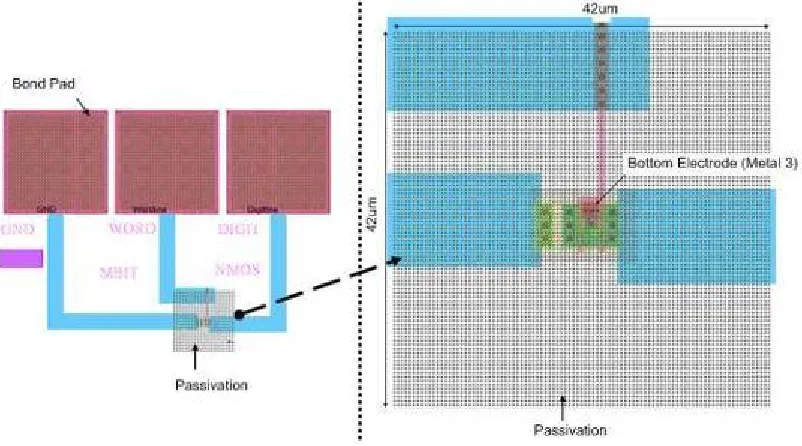
The cross sectional view of the memory bit used in the test structure is shown in Figure 2.7. Since the AMI C5 process is a three metal process, the MOSIS service is used to fabricate the device until Metal 3. The PCM bit placed on top of Metal 3 (bottom electrode) and a tungsten metal plate on top of the PCM bit (top electrode) are fabricated at the Idaho Micro Fabrication Lab. Since the chalcogenide is deposited on top of Metal 3, the size of the PCM bit depends on the size of the Metal 3 bottom electrode in the layout submitted to MOSIS.
Metal 3 Top Electrode
Chalcogenide
Figure 2.7 Cross sectional view of memory bit showing chalcogenide [2].
widths of 16 each. The size of the memory bit layout is 1.2 µm square. The layout submitted to MOSIS for the BEOL processing consists of the above said MOSFET with metal interconnects up to Metal 3 for all the four terminals (Gate, Drain, Source and Body). The Gate, Drain and Body were connected to bond pads on Metal 3 with passivation on top for external bonding. The source connection was terminated on Metal 3 with passivation on top for chalcogenide deposition.
Figure 2.8 shows the layout of a single memory bit with its corresponding terminals. A bond pad size of 75 µm by 75 µm was deemed adequate to make contacts to the Gate, Drain and the Source terminals on Metal 3. The bottom electrode size for the memory bit was chosen to be 1.8 µm by 1.8 µm and was provided on Metal 3 on the source terminal. A passivation opening of 42 µm by 42 µm was provided on top of the bottom electrode for the deposition of chalcogenide.
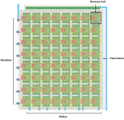
Memory Array Design and Layout
Figure 2.9 Memory array layout.
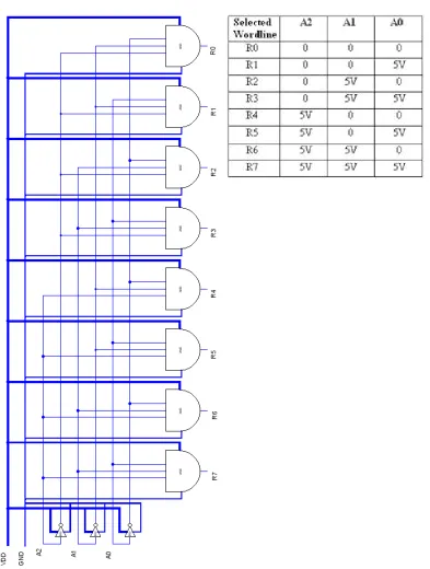
Row and Column Decoder
R
ow
S
el
ec
t
S
ign
al
s
S
el
ec
te
d
R
ow
s
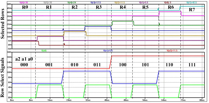
Figure 2.11 Row decoder simulations.
Figure 2.12 Column decoder schematic.
Figure 2.13 Column decoder simulations.
operation for PCRAM. Hence much effort was not put into making the design or the layout any compact. Note that the chalcogenide and Tungsten top electrode will be blanket deposited over the entire array during BEOL.
R
o
w
S
el
ec
t
C
o
lu
m
n
D
ec
o
d
er
For programming or erasing a memory cell, the row select signal makes one of the wordlines high. Similarly the column select signal connects one of the bitline to ground. A voltage higher than the threshold voltage is applied to the top electrode causing current to flow through the desired memory cell thus switching the memory cell to programmed or erased state. Similarly, during the sense operation the desired wordline is driven high using row select signals and the bitline is connected to the sense-amplifier by the column select signal. A voltage much lesser than the threshold voltage is applied to the top electrode causing a small current to flow through the memory cell. The current is small enough not to change its state. This current is used to sense the state of the memory cell and is explained in Chapter 4.
Summary
CHAPTER3:MASKDESIGNANDBACKENDOFLINEPROCESSING
The chips obtained from MOSIS were subjected to a series of post processing steps at Idaho Microfabrication Lab at Boise State University. The integration of the MOSIS fabricated chip with the post processing procedures at IML is explained in this chapter.
Figure 3.1 Bare die obtained from MOSIS. Mask Design
The mask design for the BEOL processing was performed using Electric VLSI Design System. It was then sent for fabrication to Rochester Institute of Technology Semiconductor & Microsystem Fabrication Laboratory Mask House [8]. A clear field mask tone [9] was used in the mask design for patterning the chalcogenide and top electrode. Hence the feature (chalcogenide/top electrode) in the mask is defined as being chrome and the field as clear.
Design Criteria
mask for providing site number and other details of the test structures as illustrated in Figure 3.3 and 3.4.
Figure 3.2 Layout view of chip and mask from Electric VLSI Design System.
Figure 3.3 shows the alignment of the mask for patterning chalcogenide and top electrode on the Mbit test structure while illustrating the 20 µm tolerance. Layout texts are also seen on the figure, which were included in the mask to give details about the particular test structure. It was ensured during the design that a misalignment does not cause the layout text to overlap adjacent test structures.
Figure 3.3 Layout image of an Mbit test structure showing the 20 µm tolerance of top electrode mask and the associated layout text.
Figure 3.4 Chip images of an aligned and a misaligned top electrode with bottom Chip images of an aligned and a misaligned top electrode with bottom Chip images of an aligned and a misaligned top electrode with bottom Chip images of an aligned and a misaligned top electrode with bottom electrode.
Figure 3.5 shows the aligned image of mask with the die both in design/layout view and original image seen through a microscope after post processing.
Figure 3.5 Mask and die aligned in layout/design view and from a processed die.Mask and die aligned in layout/design view and from a processed die.Mask and die aligned in layout/design view and from a processed die.Mask and die aligned in layout/design view and from a processed die.
The alignment marks on the mask are made complementary to those in the chip to align the mask and the die. Figure 3.6 shows alignment marks from the mask and chip aligned together. The alignment marks were designed with smaller error margins of 10
Figure 3.6 Alignment marks on chip and die aligned in layout view and chip image.Alignment marks on chip and die aligned in layout view and chip image.Alignment marks on chip and die aligned in layout view and chip image.Alignment marks on chip and die aligned in layout view and chip image.
A 12 to 18 µm tolerance is shown in Figure 3.7 describing the mask design for the test structure containing the memory array. Also seen the figure is layout text describing the test structure and bond pad details.
Back-End-of-Line Processing
The Back-End-of-Line processing steps were performed at Idaho Microfabrication Lab by Jennifer K. Regner, Beth Cook, Yingting Li, Hiwot Kassayebetre and Anshika Sharma of Electrical and Computer Engineering department under the guidance of Dr. Kristy A. Campbell and Dr. R. Jacob Baker. Upon receipt of the die from MOSIS, the chips were visually inspected and electrical data was collected from the transistors specifically laid out in the die for characterization. ID-VDS tests were performed and recorded to study the ID variation in the transistor which is one of the main concerns in the operation of a memory bit. This measurement also gives a base value to compare the effect of post processing steps on the transistors.
Prior to the processing steps on the die, the die is fixed to a 100 mm wafer using Ablebond epoxy 84-3 and is cured in a muffle furnace for 150 ºC for an hour to ensure proper bonding of the die to the wafer. The epoxy bonding of the die to the wafer enables easy alignment of the mask to the die using the alignment marks on the die and mask. It also makes it easier to handle the die while performing the various processing steps.
Post Processing Steps
Figure 3.9 describes the general process flow of the BEOL processing performed at Idaho Microfabircation Lab. Note that the bare die is sputter cleaned using Ar+
The die is first sputter cleaned with Ar+ to remove any metal oxides from the exposed Metal 3 due to the passivation opening. The sputtering operation is performed using a Veeco ME 1001 ion mill with 550 eV beam voltage, 300 eV source voltage, 300 mA beam current and -45o etch angle, with a process time of 6 s [10]. After sputter clean, chalcogenide films are thermally evaporated within 24 hrs. The evaporation process is done using a CHA industries SE-600-RAP evaporator with three-wafer planetary rotation at a base system pressure of 2×10⁻⁶ Torr [10]. The deposition rate is monitored with a single crystal head Inficon IC 6000. The dies are processed with different stacks of chalcogenide as described by Campbell and Anderson [11]. The memory stack consists of300 Å Germanium Selenide followed by 500 Å SnTe (Alfa Aesar) with an air break between films. Memory stacks consisting of SnSe instead of SnTe were also deposited and tested in the other dies. This step was followed by tungsten sputter to form the top electrode. The tungsten film was sputter deposited at 50 watts power, 8×10⁻⁶ Torr base pressure (350 Å), in a Sputter Sciences CrC150 single wafer tool [10].
Figure 3.10 Image of the die aligned with the mask.
Electrical Characterization
The processed die were subjected to electrical characterization prior to the BEOL processing and after the processing steps. Characterizing the transistor prior to the BEOL processing helps determine the effects of the processing steps on its operation. Figure 3.12 shows the IV curve of a 28/2 NMOS access transistor from design simulation. This simulation results are compared with the IV curves obtained from the die, pre and post BEOL processing in Figure 3.13. The electrical characterization was performed using an HP4145B semiconductor parameter analyzer. Comparing Figures 3.12 and 3.13, we see that there is not any significant effect on the electrical characteristics of the transistor from the processing steps. We also see that the model used for the simulation in Figure 3.12 during the design phase matches pretty closely with the actual IV curves obtained from the die.
Figure 3.13 IV curves for 28/2 NMOS access transistor pre and post BEOL processing [10].
To characterize the phase change material, a current was forced though a two terminal device consisting of a stack of Ge2Se3/SnSe and the voltage drop across the chalcogenide stack was measured. Figure 3.14 shows the IV curve for two terminal memory stack described above. The via size for the memory stack tested was 1.8 µm by 1.8 µm.
Figure 3.14 illustrates the possible multi state operation of the memory stack evident from the two snap-back regions. This is similar to the multi state operation described in Chapter 2 in Figure 2.3.
Sensing techniques for this resistive memory are discussed in the next chapter.
Summary
CHAPTER4:DELTA-SIGMAMODULATIONBASEDSENSING
It’s evident that chalcogenide based resistive nonvolatile phase change memory has the potential to exhibit multi state capability and hence the possibility of storing multiple bits on a single memory cell. The resistance of these states can vary from a few kΩ to several kΩ or even MΩ [2], [5]. Traditional sensing schemes use differential sensing, where the output of an “actual” cell is compared to a “dummy” cell by a differential amplifier to determine the state of the actual memory cell [12], [13]. The differential sensing scheme has major shortcomings; it is sensitive to process variations and noise, and demands wide resistance margins to sense reliably.
modulation based sensing topologies were developed and fabricated in AMI’s C5 process through the MOSIS fabrication service.
Qualitative Description of DSM Sensing Circuit
Figure 4.1 shows an example ∆Σ modulation based sensing circuit. The DSM circuit consists of an integrating capacitor Cbit (bitline capacitance), an analog to digital converter in the form of a comparator connected to the bitline and a feedback loop which acts as a digital to analog converter to maintain the bitline at a constant voltage.
The sensing circuit works on the principle of sensing the change in bitline voltage over a period due to current discharge from the sigma capacitor (bitline capacitance) through the memory cell based on its state, while using the feedback loop to maintain the bitline voltage at around a constant value. During this operation the number of times the output of the sense amp goes high ( or low) are recorded and used to determine the state of the memory cell.
Sensing Operation
The sensing begins with the bitline capacitor Cbit being charged to a voltage above the reference voltage (Vref) connected to the comparator’s negative terminal. This causes the comparator’s output terminal to turn ‘high’ thus turning OFF the PMOS switch S1, effectively cutting the supply of charge to bitline capacitance through the reference resistor Rref. Now during the sense operation, based on the current state of the memory cell (SET or RESET), the bitline voltage either stays at a constant voltage Vref or discharges to ground through the memory cell. This change in bitline voltage is due to the constant discharge of charge from the bitline capacitance Cbit through the memory cell’s resistance. Each time the bitline voltage reaches the reference voltage, the feedback loop causes PMOS switch S1 to turn back ON thus causing the sigma capacitor Cbit to charge back to a value above the reference voltage. N is recorded as the number of times the comparator is clocked and the number of clock cycles the comparator’s output stays low is recorded as M.
Considering the bitline voltage to be Vbit, the current sunk by the resistive memory element Rmbit is Imbit. The current supplied through the reference resistor Rref is Iref. Then the current supplied to the bitline capacitance Cbit is,
Iref M N
⋅ (4.1)
Since the current supplied to Cbit is equal to the current sunk by Rmbit, we can write as;
Imbit Iref M N
Now, we can write Imbit as bit mbit V
R and Iref as
( bit)
ref
VDD V R
−
, on average therefore;
bit mbit V R = M N
.( bit)
ref
VDD V R
−
(4.3)
Since Vbit is held at approximately
2
ref
VDD
V =
Rmbit N Rref M
= ⋅ (4.4)
In a real implementation of the circuit the actual resistance (Rmbit) of the memory element is not calculated, instead, a counter is employed to count the comparator output count (M) that is used to charge Cbit. This count is compared to a reference count [18] which is usually selected to represent a value between the logic 0 and logic 1 or other levels in multi level cells. Hence a count value greater than the reference count indicates one logic state and a count value less than the reference count indicates another.
DSM Circuit Components and Design Considerations
As seen in Figure 4.1, the DSM circuitry consists mainly of the integrator (Cbit), the analog to digital converter (Comparator) and the digital to analog converter (PMOS switch and resistor). The following section describes the design considerations taken into account for the design of these components for four variants of DSM sensing circuit and their effect on sensing.
Integrator
Knowing the bitline capacitance prior to the design is very crucial in the design of Delta-sigma Sense Amp (DSSA). The value of bitline capacitance Cbit and memory resistance Rmbit determines the rate of discharge of charge through the memory bit Rmbit. Meanwhile
the comparator has to be clocked prior to Cbit getting discharged completely to avoid losing the benefit of averaging. For this reason, to determine the minimum clock for the comparator, a minimum value of Rmbit is used; since the discharge rate is high for small values of resistance.
Considering the minimum value of memory resistance to be sensed as 10 kΩ, the maximum current that discharges through the memory bit when the bitline voltage (Vbit) is held at an average value of 2.5 V is,
Ibit = 250 µA (4.5) The charge stored in the bitline capacitance Cbit is,
Qbit =Cbit×Vbit (4.6)
bit bit
bit V
T C
I
= × (4.7)
Using Eq. (4.7), Table 4.1 is tablulated showing the discharge times for various bitline capacitances.
Table 4.1 Bitline capacitance discharge times for Rmbit = 10 kΩ.
Bitline Capacitance Cbit Discharge Time T
1 pF 10 ns
10 pF 100 ns
20 pF 200 ns
From the values in Table 4.1, for an Rmbit of 10 kΩ, when Ibit is maximum at 250
µA, if the bitline capacitance is 20 pF the comparator has to be clocked within 200 ns to avoid Cbit from discharging completely. Therefore a clock fclk, of 10 MHz with a time period of 100 ns would be more than adequate and fast as well. Generally, the bitline capacitance of memory array is around 3 to 5 pF. Since while testing, an additional 14 pF of capacitance is added due to the analog probe tip on the bitline, the comparator’s clock frequency is selected accordingly. While the discharging rate of the capacitor sets the minimum frequency required to clock the comparator, there is no limitation for the maximum clock frequency.
The value of bitline capacitance also has an effect on the bitline swing. This is illustrated in Figure 4.2a and b by simulating the circuit in Figure 4.1. A change in Cbit from 500 fF to 100 fF causes the ∆Vbit to change from 100 mV to 225 mV.
Analog to Digital Converter Clocked Comparator
The clocked comparator used as an analog to digital converter is a robust design with several advantages. The clocked comparator design shown in Figure 4.3 is highly sensitive to milli-volt level voltage difference on its input terminals and has high gain due to the large voltage drop across the drain to source voltage of the input transistors. The circuit does not possess memory, since prior to the sensing operation all nodes in the circuit are set to known voltages. This design also reduces kickback noise since the inputs are isolated from the output.
Figure 4.3 Clocked comparator with SR latch output.
The main draw back in this circuit is the requirement for input voltage to be above the threshold voltage of the input transistor to turn them ON. This is not a concern in this DSSA design since both the input terminals are expected to be at around 2.5 V, well above the NMOS threshold voltage. The layout of the clocked comparator is shown in Figure 4.4.
Figure 4.4 Layout of the clocked comparator.
Figure 4.5 shows the simulation results of the comparator used in DSSA. For the simulations, a ramp signal varying from 0 to 5 V is given to the negative input terminal VM while a sine wave signal from 0 to 5 V is used for the positive input terminal VP. The
Figure 4.5 Comparator simulation.
Figure 4.6 is used to determine the offset of the comparator design. For this simulation the negative input terminal is held at 2.5 V while the positive input terminal is varied from 2.4 V to 2.6 V. From the simulation result, we see that the comparator switches almost exactly when the VP reaches 2.5 V thus ensuring the 0 V offset for the comparator. Note that the comparator does not have any transistor mismatch and hence the 0 V offset. A comparator with an intentionally introduced offset will be discussed in subsequent sections.
Digital to Analog Converter and Reference Resistor
The digital to analog converter consists of a feedback circuit from the output of the comparator to a PMOS transistor which acts as a switch. The switch, when enabled connects a current source (Rref) to the bitline capacitor Cbit. During sensing, the switch is disabled and the bitline capacitance discharges through the memory cell Rmbit. Once the voltage across Cbit reaches the reference voltage Vref, the feedback loop enables the PMOS switch causing Cbit to charge by the current supplied through Rref to a voltage above the reference voltage.
Figure 4.7 Relationship between Rref, Imbit and comparator parameters.
DSM Based Sensing Topologies
Reference Resistor-Based Delta-Sigma Sensing with No Offset
The reference resistor used in the DSM topology can either be a discrete resistor or a switched-capacitor based resistor. This topology uses a discrete resistor to supply charge to the bitline capacitance. The comparator used in this topology has zero offset for switching point voltage. The topology and its associated circuit are shown in Figure 4.8.
the flexibility of the DSM topology to various resistance value of the memory cell. A reference voltage source is connected to the VCM terminal.
Figure 4.8 Reference resistor-based ∆Σ sensing circuit.
Buffers are designed at the output of the comparator to provide enough drive to retrieve the signals off chip from the bond pads. The switch S2 in Figure 4.8 is used to provide a path for the current from VDD, so that the ref node indicated in the figure does not charge up to an unknown value when S1 is OFF. In the absence of switch S2, when S1 is OFF, ref node is charged up to an unknown value. This charge is dumped on the bitline when S1 turns ON, causing a sudden increase in the bitline voltage rather than a gradual raise.
capacitor Cbit in one clock cycle T (1/fclk), Qref, should be equal to the average amount of charge sunk by the memory cell Qmbit.
Qmbit =Qref 4.10 If M is the number of clock cycles the comparator output ‘Out’ stays high out of N number times it is clocked, the relationship between charge supplied to the bitline capacitance Qref and the charge sunk by the memory cell Qmbit is given by,
Qmbit =Qref ⋅
(
M N)
4.11 Imbit⋅ =T Iref ⋅(
M N)
⋅T 4.12 Hence the average current supplied to the sigma capacitor Iref is equal to the average current sunk by the memory cell Imbit.Imbit =Iref ⋅
(
M N)
4.13
(
VDD/ 2(
⋅Rmbit)
)
=(
VDD/ 2(
⋅Rref)
)
⋅(
M N)
4.14Rmbit =Rref ⋅
(
N M)
4.15 The ratio of the number of clock cycles the comparator output goes high M, to the number of times the comparator is clocked N, gives the ratio of the reference resistance used to the resistance of the memory cell.ref
mbit
R M
for an increased number of clock cycles requiring longer sense time for higher values of Rmbit.
The minimum voltage on the bitline is
is VDD/2 + ∆Vbit. The maximum variation in bitline voltage
Figure 4.9 shows the amp without comparator offset
model the memory bit’s resistance versus sensed resistance from the DSM sense amplifier.
Figure 4.9 Simulation result for reference resistor
for an increased number of clock cycles requiring longer sense time for higher values of
The minimum voltage on the bitline is VDD/2. The maximum voltage and bitline The maximum variation in bitline voltage ∆Vbit is given by,
bit
bit ref
V C Q
∆ ⋅ ≤
bit
bit ref
V C I ⋅T
∆ ⋅ ≤
2
bit
ref bit clk
VDD V
R C ⋅ f
∆ ≤
⋅ ⋅
Figure 4.9 shows the simulation result for reference resistor-based DSM sense
amp without comparator offset. Figure 4.10 shows the plot for actual resistor used to
model the memory bit’s resistance versus sensed resistance from the DSM sense
Simulation result for reference resistor-based DSM sense amp without comparator offset.
for an increased number of clock cycles requiring longer sense time for higher values of
/2. The maximum voltage and bitline
is given by,
4.17
4.18
4.19
based DSM sense
. Figure 4.10 shows the plot for actual resistor used to
model the memory bit’s resistance versus sensed resistance from the DSM sense
Table 4.2 Reference Resistor-based ∆Σ Sense amp with no offset simulation results. Memory Cell Resistance
(kΩ)
Comparator Output Count M Calculated Resistance (kΩ)
10 250 10
20 143 17
30 100 25
40 77 32
50 63 40
60 52 48
70 45 56
80 38 66
90 35 71
100 33 76
110 29 86
120 26 96
130 25 100
140 22 114
150 21 119
160 20 125
170 19 132
180 18 139
190 17 147
200 16 156
Figure 4.10 Calculated resistances Vs Memory cell resistance for discrete reference resistor-based ∆Σ sense amp without offset.
0 20 40 60 80 100 120 140 160 180
10 30 50 70 90 110 130 150 170 190
C al cul at ed R es is ta nc e (k Ω )
Reference Resistor-Based Delta-Sigma Sensing with Offset
The voltage across the memory cell was 2.5 V in DSSA circuit topology discussed above. This voltage can sometimes cause the memory cell to switch state based on its threshold voltage as discussed in chapter 2. Minimizing the voltage across the memory cell reduces the stress across the memory element, thus avoiding the memory cell from switching state [19]. To reduce the voltage across the memory cell, a comparator with a built in offset on its reference terminal can be used. This helps in minimizing the number of reference voltages used in the sensing circuit. The comparator designed for this sensing circuit uses only VDD and VDD/2 as reference voltage and uses a built in offset to reduce the stress across the memory cell.
To add an offset to the comparator design, the size of the transistor on the reference terminal or the negative input terminal VM is made bigger than the positive input terminal VP. This imbalance requires the voltage on the positive terminal VP, to exceed VM + VOS for the comparator output to switch, where VOS is the offset of the comparator.
Figure 4.11 Simulation to determine comparator offset.
The main difference in this topology from the previous one in Figure 4.8 is the presence of an offset in the comparator and the reduction of the voltage across the memory cell from VDD/2 to VOS.
The equations governing the operation of this topology are given below. Charge is supplied to the sigma capacitor for M clock cycles out of N; hence the current through the memory cell Rmbit is given as,
os
(
(
/ 2 os)
)
(
)
mbit ref
VDD VDD V
V
M N
R R
− +
= ⋅ 4.20
Rmbit =Rref ⋅
(
Vos(
VDD/ 2−Vos)
)
⋅(
N M)
4.21 The minimum voltage on the bitline is VDD/2 + VOS. The maximum voltage and bitline is VDD/2 + VOS + ∆Vbit.. The maximum variation in bitline voltage ∆Vbit is given by,bit
bit ref
V C Q
∆ ⋅ ≤ 4.22
bit
bit ref
V C I ⋅T
∆ ⋅ ≤ 4.23
(
2 — os)
bit
ref bit clk
VDD V
V
R ⋅C f
∆ ≤
Figure 4.12 shows the simulation result for
amp with comparator offset
the memory bit’s resistance versus sensed resistance from the DSM sense amplifier.
Figure 4.12 Simulation result for reference resistor
Figure 4.13 Calculated resistances Vs Memory cell resistance for discrete reference resistor 0 40 80 120 160 200 240 280 10 30 C al cul at ed R es is ta nc e ( k Ω )
Figure 4.12 shows the simulation result for reference resistor-based DSM sense
comparator offset. Figure 4.13 shows the plot for actual resistor used to model
the memory bit’s resistance versus sensed resistance from the DSM sense amplifier.
Simulation result for reference resistor-based DSM sense amp with comparator offset.
Calculated resistances Vs Memory cell resistance for discrete reference resistor-based ∆Σ sense amp with offset.
50 70 90 110 130 150 170
Memory Cell Resistance (kΩ)
based DSM sense
tor used to model
the memory bit’s resistance versus sensed resistance from the DSM sense amplifier.
based DSM sense amp with
Table 4.3 Reference Resistor-based ∆Σ Sense amp with offset simulation results. Memory Cell
Resistance (kΩ)
Comparator Output Count M
Calculated Resistance Using Equation (kΩ)
Calculated Resistance Using Ratio (kΩ)
10 32 4 7
20 16 8 14
30 11 11 21
40 11 11 21
50 10 13 23
60 10 13 23
70 9 14 26
80 9 14 26
90 8 16 29
100 6 21 38
110 5 25 46
120 4 32 58
130 4 32 58
140 3 42 77
150 2 63 115
160 2 63 115
170 1 126 230
180 1 126 230
190 1 126 230
200 1 126 230
Switched-Capacitor Resistor-Based Delta-Sigma Sensing with No Offset
The simple reference resistors used in the first two topologies have the disadvantage of restricting the flexibility for tuning the reference resistance value once they are designed on chip. A switched-capacitor resistor built on chip has the flexibility to change the resistance value by varying the clock supplied to it.
Figure 4.14 Switched-capacitor resistor used in ∆Σ sensing circuit.
Now, considering the case when Φ1 is low and S1 is closed, the capacitor CCUP is charged to VDD. The charge stored in the capacitor during this period is,
QCUP1=CCUP⋅VDD 4.25 When S1 is open and S2 is closed, the charge stored in the capacitor is,
2
2
CUP CUP THP
VDD
Q =C ⋅ +V
4.26 It is important that M1 and M2 are not turned on at the same time. This is because we never want to connect the bitline directly to VDD.
The net charge on CCUP is given by,
2
CUP CUP THP
VDD
Q =C ⋅VDD− −V
4.27 This charge is allowed to flow into the sigma capacitor Cbit only when M3 is switched on, which is M times out of N clock cycles. Hence the average current flowing into the bitline capacitor is given by,
CUP avg
Q M
I
T N
Considering the switched-capacitor resistor’s resistance to be RSC, the average current flowing into the bilitne capacitance Cbit is,
2 THP avg
SC
VDD VDD V
I
R
− −
= 4.29
Substituting Eq. (4.28) in (4.29), we get SC 1
CUP
N R
C f M
= ⋅
⋅ 4.30 With M3 always enabled, the resistance of the switched-capacitor is,
SC 1
CUP
R
C f
=
⋅ 4.31 The two non-overlapping clocks are generated from a non-overlapping clock generator circuit shown in Figure 4.15. The clock signals Φ1 and Φ2 generated from this circuit is shown in Figure 4.16. The period of dead time between the two clock signals transitioning from high to low is labeled ∆, and is show in the figure. The value of ∆ is set by the delay through the inverter connected to the clock signal Clk. The buffers connected at the output of the circuit are to provide sharp transitioning clock signals.
Figure 4.16 Non-overlapping clock signals.
Figure 4.17 Switched-capacitor resistor-based DSM sensing circuit. The current supplied through the switched-capacitor resistor is equal to the current sunk by the memory cell. Hence,
Vref Rmbit =
(
Qcup T)
⋅(
M N)
4.32
(
VDD(
2⋅Rmbit)
)
=Ccup⋅(
VDD—VDD2) ( ) (
⋅ 1T ⋅ M N)
4.33Rmbit =
(
1(
fclk⋅Ccup)
)
⋅(
N M)
4.34 The following equations are used to determine the maximum bitline variation∆Vbit.
Ccup⋅
(
VDD VDD− 2)
= ∆Vbit⋅(
Ccup +Cbit)
4.35
(
cup(
cup bit)
)
(
2)
bit
V C C C VDD
∆ = + ⋅ 4.36
used to model the memory bit’s resistance versus sensed resistance from the DSM sense
amplifier.
Figure 4.18 Simulation result for switched
Table 4.4 Switched-capacitor resistor
Memory Cell Resistance (kΩ)
108 147 205 248 298 350 403 458 497 560 620 1000 1500 2400 4100
used to model the memory bit’s resistance versus sensed resistance from the DSM sense
Simulation result for switched-capacitor resistor-based DSM sense amp without comparator offset.
capacitor resistor-based ∆Σ sense amp without offset simulation results.
Memory Cell Resistance Comparator Output Count M
Calculated Resistance (kΩ
132 105
100 139
73 190
62 224
51 272
44 315
39 356
35 397
32 434
29 479
26 534
17 817
11 126
7 1984
4 3472
used to model the memory bit’s resistance versus sensed resistance from the DSM sense
based DSM sense amp
sense amp without offset simulation
Figure 4.19 Calculated resistances Vs Memory cell resistance for switched-capacitor resistor-based ∆Σ sense amp without offset.
Switched-Capacitor Resistor-Based Delta-Sigma Sensing with Offset
The switched-capacitor based DSM with offset has the flexibility of varying the value of the reference resistor as in the previous DSM topology. This topology also reduces the stress across the memory cell due to the comparator offset as discussed in the sensing topology “Reference resistor-based Delta-Sigma sensing with offset”. This DSM topology uses the comparator with the built in offset shown in Figure 4.11 along with a switched-capacitor resistor as the reference resistor. The comparator has a 120 mV offset which sets the voltage across the memory cell to 120 mV instead of 2.5 V, thus reducing the stress across the memory bit and avoiding unintentional program/erase operation.
The equations for this topology are similar to the topology “Reference resistor-based Delta-Sigma sensing with offset”. The only difference being the reference resistor is replaced with a switched-capacitor resistor RSC with a value derived in Eq. (4.31),
0 500 1000 1500 2000 2500 3000 3500 4000
108 205 298 403 497 620 1500 4100
C al cu la te d R es is ta n ce ( k Ω )
Substituting Eq. (4.31) in place of
The following equations are used to determine the maximum bitline variation
∆Vbit.
Ccup VDD VDD VOS Vbit Ccup Cbit
Figure 4.20 Simulation result for switched
Substituting Eq. (4.31) in place of Rref in Eq. (4.21) gives,
(
(
/ 2)
)
(
)
1os os
mbit
CUP
VDD VDD V
V M N R C f − + = ⋅ ⋅
mbit 1
(
os(
/ 2 — os)
)
(
)
cup
R V VDD V N M
C f
= ⋅ ⋅ ⋅
The following equations are used to determine the maximum bitline variation
(
2)
(
)
cup OS bit cup bit
C ⋅ VDD VDD− −V = ∆V ⋅ C +C
(
cup(
cup bit)
)
(
2 OS)
bit
V C C C VDD V
∆ = + × −
Simulation result for switched-capacitor resistor-based DSM sensing circuit with offset.
4.37
4.38
The following equations are used to determine the maximum bitline variation
4.39
4.40

![Figure 2.3 IV curve representation of a PCM bit with possible multi state capabilitycurve representation of a PCM bit with possible multi state capability [2].curve representation of a PCM bit with possible multi state capability](https://thumb-us.123doks.com/thumbv2/123dok_us/8925761.1845369/27.612.190.457.242.442/representation-capabilitycurve-representation-possible-capability-representation-possible-capability.webp)