Reversible Binary and BCD Adder Using DR
Gate
Ruchika Likhar #1, Akanksha Sinha *2
#
PG student Dept of Electronics &Telecommunication Shri Shankaracharya Technical Campus, Junwani Bhilai, Chhattisgarh
*
Assistant Professor, Dept of E&I
,
Shri Shankaracharya Technical Campus, Junwani, CSVTU university, Bhilai, Chhattisgarh , IndiaAbstract — Reversible logic is becoming one of the most promising research areas in the past few years and has being found that it is applicable in several technologies; such as low power CMOS, nanotechnology and optical computing. This is relatively new and emerging area in the field of computation which taught for thinking about computation Quantum Computing will be a total change in which computer will operate and function. The reversible arithmetic circuits are efficient regarding number of reversible gates, delay and quantum cost. Optimized design of these adders gives efficient processors. In this work we propose optimized Binary adders and BCD adders with the use of DR gate . The main purposes of designing reversible logic are to decrease quantum cost, gate count and the number of garbage outputs. The main focus is to minimize the actual resources and which provide flexibility. The proposed architecture is implemented in VHDL language using Xilinx ISE 13.2 and then it is going to be implemented in FPGA.
Keywords — Reversible logic,
DR Gate, Nanotechnology, Optical Computing
I. INTRODUCTION
Reversible
logic technology is increasins,nowadays, as a capable computing prototype with applications as emerging nanotechnologies, ultra-low power computation as Quantum dot Cellular Automata (QCA), quantum computing and optical computing.In all the reversible logic gates, the input values and output values is unique as one to one mapping. Quantum gate performs this unique one to one operation on cubits which refers to the fundamental unit of the information. The most efficient applications based on reversible logic technology lies in the quantum computations. The reversible
logic circuit should follow the following considerations:
• Bijective condition i.e, unique mapping must satisfied between the inputs and the outputs.
• No. of input signals is equal to the no. of output signals.
• The No. of garbage output vectors should be minimum.
• Constant inputs used is minimum.
Therefore, in this paper, based on the above area we developed a reversible Binary and BCD Adder using DR gate which has minimum no of gates within it and hence delay, quantum cost and power consumption is reduced when compared to reversible Binary and BCD Adder using DR gate. Simulation results in effective operations of with lesser no of gates used.
II. BASIC DEFINITIONS PERTAINING
REVERSIBLE LOGIC
A. The Reversible Logic
The n-input and k-output Boolean function f(x1, x2, x3… xn) is (referred to as (n, k) function) is called reversible if:
1. The number of outputs must be equal to the number of inputs
2. Each input pattern indicates to unique output patterns.
B. Reversible Logic Gate
Reversible Gates are the circuits in which number of outputs is equal to the number of inputs .There is a one to one mapping within the vector of inputs and outputs . It helps us to determine the outputs from the inputs as well as helps us to recover the inputs from the outputs
C.
Ancilla inputs/Constant inputs
This can be defined as the number of inputs which should be maintained constant at either 0 or 1 in order to synthesize the given logical function.
D.
Garbage Outputs
synthesisation of a given function. In rare cases these become mandatory to attain reversibility. Therefore garbage is defined as the number of outputs added to make an n-input k-output function ((n; k) function) reversible.
Constant inputs are used to denote the present
value inputs which are added to an (n; k) function to make it reversible. The following simple and easy formula shows the relationship between the number of garbage outputs and constant inputs. Input + constant input = output + garbage.E. Quantum Cost
Quantum cost can be defined as the cost of the circuit in terms of the cost of a primitive gate. It can be calculated as the number of primitive reversible logic gates (1*1 or 2*2) required to realize the circuit.
circuit is the minimum number of 2*2 unitary gates which represent the circuit keeping the output unchanged. The quantum cost of a 1*1 gate is 0 and that of any 2*2 gate is the same, which is 1.
III. REVERSIBLE GATES
Some of the important reversible logic gates are:
A. NOT Gate
The simplest Reversible gate is NOT gate and is a 1*1 gate [21]. The Reversible 1*1 gate is NOT Gate with zero Quantum Cost is as shown in the Figure 1.
Fig 1: NOT Gate
B. CNOT Gate
CNOT gate is also termed as controlled-not gate. It is a 2*2 reversible gate. The CNOT gate can be described as: Iv = (A, B) ; Ov = (P= A, Q= A^B) Iv and Ov are input and output vectors respectively. Quantum cost of CNOT gate is 1[22]. Figure 2 shows a 2*2 CNOT gate and its symbol.
Fig 2: CNOT gate
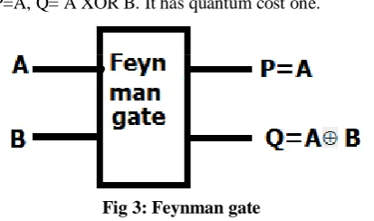
C. Feynman Gate
The Feynman gate which is a 2*2 gate and is also known as Controlled NOT and it is widely used as fan-out purposes. The inputs (A, B) and outputs P=A, Q= A XOR B. It has quantum cost one.
Fig 3: Feynman gate
D. Toffoli Gate
Fig 4 shows a 3*3 Toffoli gate. The input vector is I (A, B, C) and the output vector is O(P,Q,R). The outputs are Fig 4 shows a 3*3 Toffoli gate. The input vector is I (A, B, C) and the output vector is O(P,Q,R). The outputs are defined by P=A, Q=B, R=AB XORC. Quantum cost of a Toffoli gate is 5].
Fig 4: Toffoli gate
E. Fredkin Gate
Fig 5 shows a 3*3 Fredkin gate. The input vector is I (A, B, C) and the output vector is O (P, Q, R).
The output is defined by P=A, Q=A′BXORAC and R=A′CXORAB. Quantum cost of a Fredkin gate is
4.
Fig 5: Fredkin Gate
F. Peres Gate
Fig 6: Peres Gate
IV. LITERATURE REVIEW
Harpreet Singh, Chakshu Goel proposed an
optimised reversible full adder-subtractor design called “WG gate”. Design of reversible gates is inhanced by reducing its parameters like quantum cost, garbage outputs, etc. but this proposed gate is optimised regarding quantum cost and should be used in various adder-subtractor circuits. Although this paper supplies only an elementary component which is used to perform arithmetic calculation, yet more complicated circuits can be easily built using the reversible logic.
V.Kamalakannan, Shilpakala.V, Ravi.H.N
suggested that a design of Reversible Binary Adder-Subtractor- Mux, Adder-Adder-Subtractor- TR Gate., Adder-Subtractor- Hybrid are proposed. In all the design approaches, the Adder and Subtractor are realized in a single unit with compare to only full adder/subtractor in the existing design. The performance analysis is verified using number of reversible gates, Garbage input/outputs and Quantum Cost.The reversible 4-bit full adder/ subtractor design unit is get compared with conventional ripple carry adder, carry look ahead adder, carry skip adder, Manchester carry adder are based on their performance with respect to area, timing and power constraint. Hence the proposed work is beneficial in low power applications where both adder and subtractor units are required.
Abinash Kumar Pala , Jagamohan Das proposes reversible logic implementation of the 4- bit adder which is optimized to obtained minimum number of logic gates and garbage outputs. This project is being worked on the reversible 4-bit adder circuits designed and proposed here to form the basis of the decimal ALU of a primitive quantum CPU. The designed and optimized 4-bit reversible adder is then implemented in VHDL Using Xilinx ISE 12.1 tool. Nagamani A N, Ashwin S, Vinod Kumar Agrawal proposes a reversible binary adder and subtractor design with an optimized quantum cost and delay with compared to previous work in literature and using this adder, an optimized reversible BCD adder in terms of Quantum cost, delay and garbage outputs which have been designed using reversible gate libraries made in Verilog model and functionally verified using Xilinx ISE tool. The use of negative control lines in the design for detecting overflow logic of BCD adder has considerably reduced delay and gate count which result in high speed BCD
adder with optimized area. Thus we can be conclude that the use of Negative control linesresults in reduction of the gate count and hence area, which gave us several way to lot of scope in the field of reversible computing in near future.
Rangaraju H G, Venugopal U, Muralidhara K N: proposes Reversible eight-bit Parallel Binary Adder/Subtractor unit. The Design I, Design II and Design III are used to implement half and full Adder/Subtractor. The Reversible eight-bit Parallel Binary Adder/Subtractor are built using three designs. The Design III implementation of Reversible eight-bit Parallel Binary Adder/Subtractor performed better as compared to Design I, Design II and existing design in terms of number of gates used, Garbage inputs/outputs and Quantum Cost, hence can be used as low power applications. The full Adder/Subtractor is implemented on a single unit as compared to only full Subtractor in the existing design [5]. In future, the design can be extended to any number of bits for Parallel Binary Adder/Subtractor unit and also for low power Reversible ALUs, Multipliers and Dividers.
Aribam Balarampyari Devi, Manoj Kumar and Romesh Laishram : A modified carry increment adder is proposed in the paper using this faster carry look ahead modules instead of the much slower ripple carry adder. By replacing the 4-bit RCA with a 4-bit CLA the delay performance of the circuit is inhanced in the design without affecting the power dissipation of the circuit. The design is tested and verified by Verilog HDL coding and simulation is implemented in Xilinx ISE 13.1 environment.
V. COMPARITIVE STUDY
Comparison Between Reversible Logic Gates
VI. CONCLUSION
In this work, we proposed a reversible binary adder design with optimized quantum cost and delay some other constraint as compared to previous work in literature and using this adder, an optimized reversible BCD adder and Binary adder in terms of Quantum cost, delay and outputs have been designed. All the designs are functionally verified using Xilinx ISE tool. The improvement in elementary parameters is worked upon in the modern research. In the proposed work, out of all elementary parameters, the parameter termed as quantum cost is reduced by generating a design which uses less number of elementary gates and resulting in a quantum cost of 7, compared with the quantum cost of 8 achieved in the existing work.
References
[1] M.A. Nielsen, I.L. Chuang, “Quantum Computation and Quantum Information,” Cambridge University Press p. 13, Cambridge, 2000
[2] R. Landauer, “Irreversibility and heat generation in the computational process,” IBM journal of research and development, vol. 5, issue 3, pp. 183–191, July 1961. [3] R. Keyes, R. Landauer, “Minimal energy dissipation in
logic,” IBM Journal of Research and Development, vol. 14, issue 2, pp. 153–157, Mar. 1970.
[4] C.H. Bennett, “Logical reversibility of computation,” IBM J. Res. Dev., vol. 17, issue 6, pp. 525–532, Nov. 1973. [5] Gordon E. Moore, “Cramming More Components onto
Integrated Circuits,” Electronics, pp. 114–117, April 19, 1965.
[6] F.Q. Xie, L. Nittel, T. Schimmel, et.al. , Phys. Rev. Lett. 93, 128303, Sep. 2004.
[7] H.G. Rangaraju, U. Venugopal et.al. , “Low power reversible parallel binary adder/subtractor,” International Journal of VLSI Design & Communication Systems, pp-23-34, arXiv: 1009.6218, 2010.
[8] P. Kaur, B.S. Dhaliwal, “Design of Fault Tolearnt Full Adder/Subtractor Using Reversible Gates,” 2012 International Conference on Computer Communication and Informatics (ICCCI-2012), Coimbatore, Jan. 10 – 12, 2012. [9] S. Sultana and K. Radecka, “Reversible Adder/Subtractor
with Overflow Detector,” IEEE 54th International Midwest Symposium on Circuits and Systems (MWSCAS), Aug. 2011.
[10] A.K. Biswas et.al, “Efficient approaches for designing reversible Binary Coded Decimal adders,” Microelectronics journal, vol. 39, issue 12, pp.1693-1703, December 2008. [11] Ri-gui Zhou, Man-qun Zhang, Qian Wu, Yan-Cheng Li,
“Optimization Approaches for Designing a Novel 4-Bit Reversible Comparator,” Int. J. of Theoretical Physics, 52, pp. 559-575, 2013.
[12] Md. Saiful Islam and Md. Rafiqul Islam, “Minimization of Reversible Adder Circuits,” Asian Journal of Information Technology, Vol. 4, No. 12, pp. 1146-1151, 2005. Rahman, Saiflil Islam, Zerina Begum, Hafiz, Mahmud, "Synthesis of Fault Tolerant Reversible Logic Circuits", IEEE, 978-1-4244-2587- 7/09,2009.
[13] Kamalika, Gaurav, Wille, "Exploiting Negative Control Lines in the Optimization of Reversible Circuits", Springer- Verlag Berlin Heidelberg 2013.
[14] H. M.H. Babu and AR. Chowdhury. "Design of a compact reversible binary coded decimal adder circuit". Elsevier Jour. of Systems Architecture, 52:272-282, 2006.
[15] Ashis Kumer Biswas, Md. Mahmudul Hasan, Ahsan Raja Chowdhury, and Hafiz Md. Hasan Babu. "Efficient approaches for designing reversible binary coded decimal adders".Microelectron. 1., 39(12): 1693- 1703,2008. [16] M.K. Thomsen and R.Gruck. "Optimized reversible
binary-coded decimal adders". 1. Syst.Archit., 54(7):697-706, 2008.
[17] M. Mohammadi, M. Eshghi, M. Haghparast, and A Bahrololoom."Design and optimizationof reversible bcd adderlsubtractor circuit for quantum and nanotechnology based systems".World Applied Sciences Journal, 4(6):787-792, 2008.
[18] M. Mohammadi, M. Haghparast, M. Eshghi, and K. Navi. "Minimization optimization of reversible bcd-full adderlsubtractor using genetic algorithm and don't care concept". InternationalJ. Quantum Information, 7(5):969-989, 2009.
[19] Himanshu Thapliyal and Nagarajan Ranganathan, "Design of Efficient Reversible Logic based Binary and BCD adder circuits", ACM Journal on Emerging Technologies in Computing Systems, Vol. 9, Issue 3, September 2013. [20] H.R. Bhagyalakshmi and M.K. Venkatesha, "Optimized
reversible BCD adder using new reversible logic gates", Journal of Computing, Volume 2, Issue 2, February 2010, ISSN 2151-9617.
REVERSIBLE GATES
QUANTUM COST
TYPES
FEYNMAN GATE[23]
1 2*2
TOFFOLI GATE[24] 5 3*3
FREDKIN GATE[6] 5 3*3
PERES GATE[7] 4 3*3
TSG GATE[25] 4 4*4
URG GATE[26] UNKNOWN 3*3
SYSTEM GATE[27] UNKNOWN 4*4
TR GATE[26] 6 3*3
NFT GATE[26] 5 3*3
BJN GATE[26] 5 3*3
MTSG GATE[25] 6 4*4
BME GATE[26] 5 4*4
SAYEM GATE[13] UNKNOWN 4*4
VB-1 GATE[28] UNKNOWN 4*4
VB-2 GATE[28] UNKNOWN 4*4
[21] Hafiz Md. Hasan Babu and Ahsan Raja Chowdhury, "Design of a Reversible Binary Coded Decimal Adder by using Reversible 4-bit Parallel Adder ", Proceedings of the 181h International Conference on VLSI Design and 4th International Conference on Embedded Systems Design, 1063-9667/05, IEEE 2005.
[22] K. V. R. M. Murali, N. Sinha, T. S. Mahesh, M. H. Levitt, K. V. Ramanathan, and A Kumar. "Quantum information processing by nuclear magnetic resonance: experimental implementation of half-adder and subtractor operations using an oriented spin"-7/2 system. Physical Review A, 66(2):022313, 2002.