DTMOS based Second Generation Current
Conveyor Topologies Comparison
Monal Gupta Bhawna
M. Tech Student M. Tech Student
Department of Electronics and Communication Engineering Department of Electronics and Communication Engineering
Indira Gandhi Delhi Technical University for Women, Kashmere Gate, Delhi, India
Indira Gandhi Delhi Technical University for Women, Kashmere Gate, Delhi, India
Prof. Ashwani Kumar
Professor
Department of Electronics and Communication Engineering
Indira Gandhi Delhi Technical University for Women, Kashmere Gate, Delhi, India
Abstract
In this project three different topologies of second generation current conveyor (CCII) have been explained. Current conveyor is a high performance analog circuit design block based on current mode and voltage mode approach. It is basically a unity gain element that exhibits high linearity, wide dynamic range, high bandwidth and better high frequency response. For low voltage low power applications we have used the DTMOS technique in these CCII topologies. The circuits are operated at a low voltage of ±0.5V. PSPICE simulation results using TSMC 0.18μm CMOS technology have been presented for the proposed circuits. We find that the linearity, frequency response have improved using DTMOS technique and the power consumption of the circuits has reduced which has been shown using the simulated results.
Keywords: DTMOS Technique, Translinear loop, Differential Pair, CCII
________________________________________________________________________________________________________
I. INTRODUCTION
Current Conveyor has emerged as one of the promising current mode circuits which has replaced the traditional voltage mode op-amp circuits. It gives high performance in terms of the operation at low voltage with higher dynamic range, simple structure, greater linearity and better frequency response. The current mode circuits are faster as compared to the voltage mode circuits due to the less parasitic capacitances. They give us reliable mode of operation and are simpler in design. Among three generations of current conveyor, second generation current conveyor (CCII) proved to be a high performance circuit which gives reliable performance in the design of low voltage low power circuit [1]. To extend the lower bound of power supply to ultra-low voltage we have used the DTMOS technique which makes the circuit to be operated at voltages below 0.6volts.
The DTMOS technique serves us with several advantages in low-voltage analog circuits. First, in low-voltage applications there is not much voltage headroom for signal swing and reducing the threshold voltage can be helpful. Second, having a fourth terminal can be advantageous since it can result in a simpler circuit with a fewer number of transistors. Third, the voltage range at the body terminal of a PMOS transistor normally covers the range of voltages which is not covered by the gate of the transistor. Therefore, using the bulk terminal makes it possible to extend the input voltage range of a circuit [5].
II. SECOND GENERATION CURRENT CONVEYOR
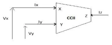
The second generation current conveyor (CCII) is one of the most versatile current mode building blocks. It was introduced by Sedra in 1970 in succession with first generation current conveyor. Due to its high impedance at one input node and low impedance at other input node, it finds a huge number of applications in various areas. As compared to CCI which consisted two low impedance nodes, this CCII is preferable to avoid the loading effect. The basic block representation of second generation CC can be given as
This current conveyor differs from the first generation current conveyor in a sense that the port Y is a high impedance port i.e. there is no current flowing into port Y. The port Y of the second generation current conveyor is used as a voltage input and port Z is used as a current output port. Whereas, the port X can be used as a voltage output or as a current input port. Therefore, this current conveyor can be used to process both voltage and current signals. In matrix form, the relation between terminals X, Y and Z can be shown as:
Thus, the voltage following and current following action in various applications can be accomplished using the CCII efficiently. In general there are two types of CCII:
Positive current conveyor (CCII+) in which there is same direction of current flowing from port X and port Z
Negative current conveyor (CCII-) in which the direction of current at X port is opposite to that of the current at Z port. CCII finds its variety of applications in various useful circuits such as amplifiers, analog computing, filters, nonlinear applications, oscillators.
III. DTMOS TECHNIQUE
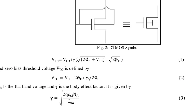
Dynamic threshold mosfet (DTMOS) transistor was proposed by Assederaghi et al in 1994. The dynamic threshold MOS transistor (DTMOS), proposed in [3] , is very suitable to be employed in circuits to be used in ultra-low voltage environment. In DTMOS, body terminal is tied to gate terminal making threshold voltage of MOS transistor (VTH), a function of the gate input.
Fig. 2: DTMOS Symbol
VTH= VTO+γ(√(2∅F+ VSB) - √2∅F ) (1) And zero bias threshold voltage VTOis defined by
VTO = VFB+2∅F+ γ√2∅F (2) VFBIs the flat band voltage and γ is the body effect factor. It is given by
γ = √2qεSiNA
Cox
(3)
In this device, the threshold voltage of the device is a function of its gate voltage, i.e. as the gate voltage increases the threshold voltage (VTH) drops resulting in a much higher current drive than standard MOSFET for low-power supply voltages. On the other hand, VTH is high at VGS = 0, therefore the leakage current is low. Thus the DTMOS technique allows the lowering of the supply voltage by reducing the threshold voltage dynamically. Due to dynamic body bias, potential in the channel region is strongly controlled by the gate and body terminals, leading to a high transconductance owing to faster current transport. Since the transconductance of the DTMOS is greater than the conventional CMOS transistor, the frequency bandwidth for the DTMOS increases with the increase in the transistor transconductance.
IV. DTMOS BASED CCIITOPOLOGIES
Proposed Translinear Loop Based CCII Using DTMOS
along with a push pull stage as the output stage is considered to be the best [4]. The push pull stage specifically enhances the current handling capability of the conveyor side by side maintaining the high output impedance level
This translinear loop based CCII has been modified by using the DTMOS technique in all the transistors where we have connected the body terminal of MOS transistor to the gate terminal. This will allow the circuit to operate at a low voltage supply. This circuit has been operated at the symmetric supply of ±0.5 V. The circuit is biased using the current biasing source of Ibias.
Fig. 3: Translinear Loop based CCII using DTMOS Technique
The transistors M1-M4 and M7-M8 are used to form translinear loop and current mirror respectively. At node X, the two currents namely bias current Ibias and input current Iin are injecting at node and is entering into transistor with current. The transistors M1-M2, M10-M12 are used for proper biasing. At node, is out-going current and is incoming current. On applying KCL at node Z, the current is equal to the translinear loop based second generation current conveyor schematic is shown in figure 3.The translinear CCII depends on tight matching of the NMOS and PMOS paths to achieve higher linearity and reduce offsets.
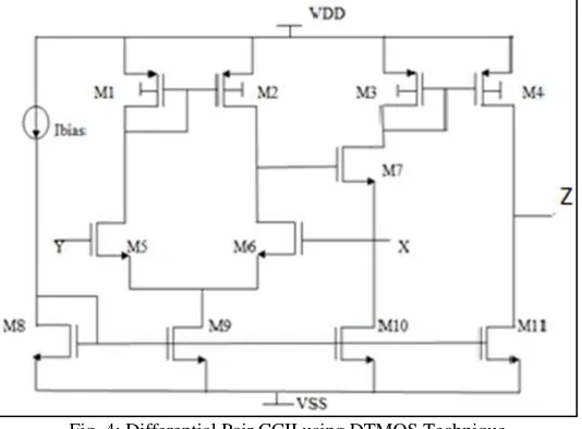
Proposed Differential Pair Based Second Generation Current Conveyor
The differential pair based current conveyor is shown in figure 4. The circuit between ports Y and X allows the function of voltage follower and between ports X and Z allows the function of current follower. PMOS transistors M1-M4 has been replaced by the DTMOS transistors in which body is tied to the gate terminal.
Fig. 4: Differential Pair CCII using DTMOS Technique
the current transfer accuracy, increasing the output current capabilities, while reducing the offset using several compensation techniques and capable of operating under a minimum supply voltage at the input stage and at the output stage.
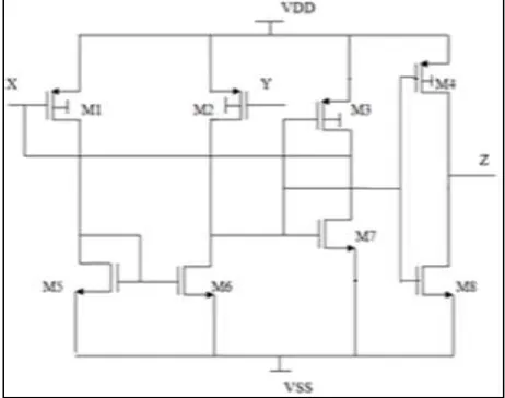
Proposed Differential Pair Based 8-T Second Generation Current Conveyor
As the technological advancements are being done in terms of the miniaturization of the integrated circuits, we are moving towards the smaller circuits. The differential pair based second generation current conveyor described here consists of 8 transistors. The structure has some of the advantages of higher offset.
Fig. 5: 8-T Differential Pair based CCII using DTMOS Technique
Transistors M1-M4 are PMOS transistors and transistors M5- M8 are conventional NMOS transistors whose body terminal is grounded. Transistor M1-M2, M5-M6 forms the input differential stage. M4 & M8 form the class AB output stage. The advantage of this class AB output stage is to offer high dynamic range and good linearity for low power consumption. There is a feedback through transistor M7 which helps in reducing the X input terminal resistance which should ideally be zero. This circuit has three terminal devices X, Y and Z where the input voltage applied to terminal Y is perfectly conveyed to X terminal and the input current at X terminal is conveyed to the Z terminal with the same direction if CCII is positive (CCII+) or reverse direction, if CCII is negative (CCII-). According to current copying property of plus type CCII, current at port X and port Z is same in magnitude and direction i.e., IZ1=IX.
V. SIMULATION AND COMPARISON RESULTS
Simulation of proposed circuits has been done using the 0.18um CMOS technology. Using the DTMOS technique there have been improvements with respect to the linearity, bandwidth and accuracy between the input and output signals of the circuits.
Proposed- I CCII
Sinusoidal Response:
Transient analysis has been performed in order to obtain the voltage transfer characteristics between the ports Y and X with respect to time. It is performed by applying the sinusoidal signal at the port Y of amplitude 0.1V peak-to-peak and its response at the port X is shown in the figure 6.
DC Analysis:
Dc analysis has been performed in order to obtain the voltage transfer characteristics between the ports X and Y and current transfer characteristics between the ports X and Z. In dc analysis we have given the dc input voltage of 0.1V at the port Y and with respect to this we have observed the variation of output voltage at the port X. This type of characteristics gives us the performance analysis of the linearity of the circuit. Input linear range of the proposed circuit has increased and found to be -66.94Mv to 104.12mV as shown in figure 7.
Fig. 7: Variation of Voltage at Vx by Varying the Voltage at Vy
AC Response:
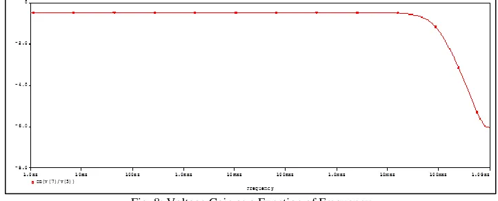
The frequency response of the voltage gain at port X is shown in the figure 8 .Variation of Vx/Vy with respect to the frequency is performed which shows the magnitude close to unity. 3dB bandwidth has improved to 280MHz.
Fig. 8: Voltage Gain as a Function of Frequency
Proposed-II CCII
Sinusoidal Response:
Sinusoidal response is obtained by applying the sinusoidal signal at the port Y of amplitude 0.1V.
DC Analysis:
Input linear range has increased using DTMOS and found to be -517.105mV to 270.49mV
Fig. 10: Variation of voltage at Vx by varying the voltage at Vy
AC Response:
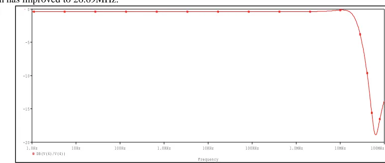
3dB bandwidth has improved to 26.69MHz.
Fig. 11: Voltage Gain as a Function of Frequency
Proposed-III CCII
Sinusoidal Response
Sinusoidal response is obtained by applying the sinusoidal signal at the port Y of amplitude 0.1V.
Fig. 12: Plot of Vx Vs Vy
DC Analysis:
Input linear range is found to be -191mV to 55.28mV
Frequency
1.0Hz 10Hz 100Hz 1.0KHz 10KHz 100KHz 1.0MHz 10MHz 100MHz
DB(V(6)/V(4)) -20
Fig. 13: Variation of voltage at Vx by varying the voltage at Vy
AC Response:
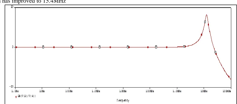
3dB bandwidth has improved to 15.4MHz
Fig. 14: Voltage Gain as a Function of Frequency
Table - 1 Comparison Table
Parameters CCII [4] CCII [2] CCII [3]
Technology 180nm 180nm 180nm
Supply voltage ±0.5V ±0.5V ±0.2V
Input linear range -66.94mV to 104.12 -517.105mV to 270.49mV -191.4mV to 55.2mV
3dB bandwidth 280MHz 26.6MHz 15.4MHz
Power Consumption (μW) 13.1 13.8 14.3
Table - 2
Power Consumption of DTMOS Based Topologies DTMOS based CCII Topology Power Consumption (μW)
Translinear CCII 13.1
Differential pair CCII 13.8 8-T differential pair CCII 14.3
VI. CONCLUSIONS
We have performed the detailed analysis of three CCII based structures namely translinear loop based CCII, differential pair based CCII and differential pair using 8-T. All the three topologies have been proposed for the low voltage low power design using the DTMOS technique. The simulations have been carried out using PSPICE with 0.18μm technology parameters. The simulation results have been shown to demonstrate the feasibility of the circuits. A comparison has been done for all the three topologies which clearly show that using the DTMOS technique, the power consumption has been reduced to a great extent with the circuits operating at a low voltage supply of ±0.5volts. The bandwidth and linearity of the circuits has also been improved using the DTMOS.
Vy
-400mV -350mV -300mV -250mV -200mV -150mV -100mV -50mV 0mV 50mV 100mV 150mV 200mV 250mV 300mV 350mV 400mV V(4) V(2)
REFERENCES
[1] A. S. Sedra and K. C. Smith, “A Second-Generation Current Conveyor and Its Applications”IEEE Trans. on Circuit Theory, vol. 17, no. 1, pp. 132-134, 1970. [2] W. Surakampontorn, V. Riewruja, K. Kumwachara, and K. Dejhan, “Accurate CMOS Based Current Conveyors, " IEEE Transactions on Instrumentation
and Measurement, vol. 40, no. 4, pp.699–702, 1991.
[3] A. Uygur, H. Kuntman,“An ultra-low-voltage, ultra-low-power DTMOS-based CCII design for speech processing filters,” Proc. Of ELECO 2013: The 8th International Conference on Electrical and Electronics Engineering, pp.31-35, Bursa, Turkey, 2013.
[4] G. Varshney, N. Pandey, R. Pandey and A. Bhattacharyya, "Performance comparison of filter circuits based on two different current conveyor topologies," 2013 International Conference On Signal Processing And Communication (ICSC), Noida, 2013, pp. 419-423.
[5] F. Assaderaghi, D. Sinitsky, S.A. Parke, et. al.,"Dynamic threshold voltage MOSFET (DTMOS) for ultra-low voltage VLSI," IEEE Transactions on Electron Devices, vol. 44, no.3, pp. 414-422,1997.
[6] V. Niranjan, A. Singh, A. Kumar, “Dynamic Threshold MOS transistor for Low Voltage Analog Circuits,” International Journal of Scientific Research Engineering & Technology (IJSRET), vol. 1, pp. 26-31, August 2014.
[7] Prerna and V. Niranjan, "Analog multiplier using DTMOS-CCII suitable for biomedical application," International Conference on Computing, Communication & Automation, Noida, 2015, pp. 1353-1357.
[8] A. M. Ismail and A. M. Soliman, “Wideband CMOS current conveyor," Electronics Letters, vol.34, no.25, pp.2368–2369, 1998. [9] Smith K C and Sedra A: “The current conveyor – new building block”, IEEE Proc., 1968, 56, pp. 1368-1369.