ISSN: 2393-8366
711
Test Pattern Generation for Jump Bit Insertion in Scan
Diagnosis
Dona Mariya Thomas1, S. Krishna Kumar2
1
PG Scholar, Department of Electronics and Communication Engineering, Federal Institute of Science and Technology, Mookkannoor, Kerala, India. Email: [email protected]
2
Professor, Department of Electronics and Communication Engineering,Federal Institute of Science and Technology, Mookkannoor, Kerala, India
Email:[email protected]
Abstract: Scan chain failures accounts for about 30% of chip failures. Scan chain diagnosis is complex because of limited observability. A single scan chain consists of large number of flip-flops (scan cells). Scan chain diagnosis approaches identify candidate cells. All the methods developed so far attempts to reduce the range of candidate cells, by identifying an upper bound and a lower bound. In this paper we propose a method to identify the candidate cell by bit insertion and simulation technique. The effectiveness of the approach is verified by experiments on ISCAS’89 benchmark circuits.
Keywords--- Testing, diagnosis,scan architecture, flush test, capture cycle.
1. INTRODUCTION
A circuit consists of both combinational logics and sequential blocks. Before we ship the design it is to be verified that the circuit is functionally accurate and is free from any manufacturing defect. Faults in a circuit can be systematic errors, which arise due to some extra connections or missing connections, or random errors, which is the result of some environmental conditions in which the circuit is placed. Random errors cannot be identified and rectified, but systematic errors can be rectified [1]. In a circuit, faults can occur in both combinational logics and sequential blocks. 70% of circuit faults are due to faults in combinational logic, which can be tested and diagnosed using any of the algorithms like D algorithm, PODEM algorithm, FAN algorithm, etc [2]. Rests 30% of faults are due to the sequential blocks. There are several testing methods to identify the type of fault [3] [4] [5] [6] [7]. Diagnosis of flip-flip-flop is tedious. Taking out pins from flip-flop to observe each flip-flop in circuit can be tried for small circuits. For circuits containing large number of flip-flops, driving out pins is impractical.
ISSN: 2393-8366
712
during a 0 to 1 transition or a 1 to 0 transition. Different transition fault models are, (a) Slow to Rise Fault (b) Slow to Fall Fault (c) Fast to Rise Fault (d) Fast to Fall Fault [8]. Flush test is used to identify the fault type in a scan chain [6] [9].
Diagnosis aims at identifying a list of suspect faulty scan cells. The diagnosis methods are classified into Tester based method, Hardware based method [1] [10] [11] [14] and Software based method [5] [6] [7] [9] [12] [13] [14] [15] [16] [17] [18]. Hardware methods demand hardware overhead, which in turn increases the total circuit area
This paper is divided into four sections. The first section discuss about the fault diagnosis in scan chain using Jump simulation [18]. The second section discuss about the test pattern generation to carry out Jump simulation. The third section discusses the results and discussions. Finally, the last section is a brief conclusion about the work done.
2. PROPOSED METHOD DIAGNOSIS OF SINGLE STUCK AT FAULT IN SINGLE SCAN CHAIN
The fault diagnosis of scan chain is carried out in two phases. In the first phase, flush test (11001100 pattern is used) identifies the faulty scan chain and the fault type. In the second phase, Jump simulation identifies faulty scan cell in the faulty scan chain.
2.1 Jump Simulation
After finding the faulty scan chain and fault type, the fault diagnosis is carried out using Jump Simulation. The following steps elaborate Jump simulation:
1. Start.
2. Run combinational logic, and find the upper bound and lower bound.
3. Insert jump bit (jump bit 1 for stuck at 0 (SA0) and jump bit 0 for stuck at 1 (SA1)) in scan cell very next to the left of the lower bound.
4. Compare the bit with the jump bit inserted to the scan cell.
5. If a fault is diagnosed, stop the simulation. If the fault is not diagnosed, carry out step 3 and 4 for all other scan cell to the left of previously taken cell, up to the upper bound till the fault is diagnosed.
6. Stop.
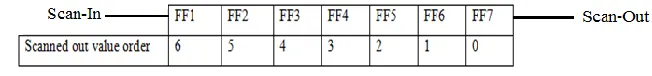
The algorithm is illustrated with an example. Seven flip-flops in the scan chain of ISCAS‟89 s386 benchmark circuit are arranged as a scan chain as shown in Fig. 1.
Fig. 1 Scan Chain of ISCAS‟89 S386 Benchmark Circuit
The Jump simulation is carried out in two phases.
ISSN: 2393-8366
713
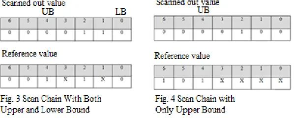
In this phase the upper bound (UB) and lower bound (LB) is identified. The response of fault free circuit (golden response) for a particular test pattern is computed prior to diagnosis. Phase 1 includes four steps: (1) Apply test pattern (2) Combinational logic simulation (3) Capture cycle (4) Scan out.
The scanned out value is compared with the golden response. The comparison starts from right (Flip-flop near to Scan-Out) to left (Flip-flop near to Scan-In) of the scan chain. The first scanned out value that matches with the fault free response is noted and the corresponding scan cell is marked as the lower bound. The first scanned out value that mismatches with the fault free response is noted and the corresponding scan cell is marked as the upper bound. This is shown in the Fig. 2.
Fig.2 Identification of Upper Bound and Lower Bound
It is definite that the fault lies within the lower and upper bound, or the upper bound itself is faulty. Finding bounds reduces the suspect or the candidate list.
Phase 2:
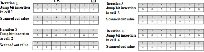
The jump bit is inserted in this phase. In this phase, only scan cells within the upper and lower bound, and the upper bound is considered.
ISSN: 2393-8366
714
scan cells 1 and scan cell 6, or the scan cell 6 itself can be faulty. To check which scan cell is faulty the jump bit is inserted. The jump bit insertion is shown in Fig. 5.
Fig. 5 Jump Simulation Example for Scan Chain with Both Upper and Lower Bound
A scan chain with the upper bound alone, the jump bit insertion starts from the first scan cell from the right of the scan chain. The rest, all diagnosis procedure is same as that of a scan chain with both upper and lower bound. During the phase 1 and phase 2 of Jump simulation, values are to be inserted into the flip-flops. For that input test patterns are required. This test pattern generation is discussed in the next section.
3. TEST PATTERN GENERATION
To carry out phase 1 and phase 2 of Jump simulation, test patterns have to be generated. The input test patterns are applied to simulate the combinational logic to force states (values) into the flip-flops. The golden response, for the corresponding test vectors will be used as reference in first phase of Jump simulation. A combinational automatic test pattern generator, Atalanta [24] can be used to generate input test patterns and its corresponding output responses. Atalanta takes the circuit netlist and the fault list as inputs and generates the test pattern for the faults listed and the corresponding golden response. Atalanta being a combinational test pattern generator, the flip-flops have to be removed from the netlist. The inputs of flip-flops form the pseudo primary outputs and outputs of flip-flops form the pseudo primary inputs (if it feed some logic gates). The original ISCAS‟89 netlist is modified to accommodate these changes. Specifying fault list for pseudo primary outputs is as good as inserting the faults (stuck at 0 and stuck at 1) at the corresponding flipflop. Atalanta generates input test patterns for activating the fault in the flipflop. Fault simulation also gives the primary output values for the corresponding input test pattern.
4. RESULTS AND OBSERVATIONS
ISSN: 2393-8366
715
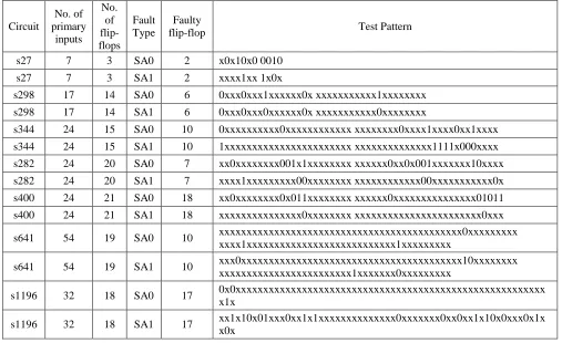
flip-flop 2 (candidate flip-flop), then a stuck at 0 fault is included in the fault list fed to Atalanta. The corresponding test pattern generated is shown in column 6.
Table 1 Test Pattern Generated for Different Faulty Flip Flops
Circuit
No. of primary
inputs No.
of flip-flops
Fault Type
Faulty
flip-flop Test Pattern s27 7 3 SA0 2 x0x10x0 0010
s27 7 3 SA1 2 xxxx1xx 1x0x
s298 17 14 SA0 6 0xxx0xxx1xxxxxx0x xxxxxxxxxxx1xxxxxxxx s298 17 14 SA1 6 0xxx0xxx0xxxxxx0x xxxxxxxxxxx0xxxxxxxx
s344 24 15 SA0 10 0xxxxxxxxxx0xxxxxxxxxxxx xxxxxxxx0xxxx1xxxx0xx1xxxx s344 24 15 SA1 10 1xxxxxxxxxxxxxxxxxxxxxxx xxxxxxxxxxxxxx1111x000xxxx s282 24 20 SA0 7 xx0xxxxxxxx001x1xxxxxxxx xxxxxx0xx0x001xxxxxxx10xxxx s282 24 20 SA1 7 xxxx1xxxxxxxxx00xxxxxxxx xxxxxxxxxxxx00xxxxxxxxxxx0x s400 24 21 SA0 18 xx0xxxxxxxx0x011xxxxxxxx xxxxxx0xxxxxxxxxxxxxxx01011 s400 24 21 SA1 18 xxxxxxxxxxxxxxx0xxxxxxxx xxxxxxxxxxxxxxxxxxxxxxx0xxx s641 54 19 SA0 10 xxxxxxxxxxxxxxxxxxxxxxxxxxxxxxxxxxxxxxxxxxxx0xxxxxxxxx
xxxx1xxxxxxxxxxxxxxxxxxxxxxxxxxx1xxxxxxxxx
s641 54 19 SA1 10 xxx0xxxxxxxxxxxxxxxxxxxxxxxxxxxxxxxxxxxxxxxx10xxxxxxxx xxxxxxxxxxxxxxxxxxxxxxxx1xxxxxxx0xxxxxxxxx
s1196 32 18 SA0 17 0x0xxxxxxxxxxxxxxxxxxxxxxxxxxxxxxxxxxxxxxxxxxxxxxxxxxxxxxxx x1x
s1196 32 18 SA1 17 xx1x10x01xxx0xx1x1xxxxxxxxxxxxxx0xxxxxxx0xx0xx1x10x0xxx0x1x x0x
5. CONCLUSION
In this paper we have proposed a method to generate test patterns for inserting jump bits in candidate cells. This approach is effective in identifying the faulty scan cell in a scan chain with single fault. This approach can be easily adapted to identify the faulty scan cell in an architecture supporting multiple scan chains.
REFERENCES
[1]Subhadip Kundu, Satanu Chattopadhyay, Indranil Sengupta, and Rohit Kapur, “Aggressive Scan Chain Masking For Improved Diagnosis Of Multiple Scan Chain Failure,” 18th IEEE European Test Symposium, 2013.
[2] MuralidharanVenkatasubramanian, Vishwani D. Agrawal, “Quest for a Quantum Search Algorithm for TestingStuck-at Faults in Digital Circuits,” IEEE International Symposium on Defect and Fault Tolerance
ISSN: 2393-8366
716
[3] Subhadip Kundu,Santanu Chattopadhyay,Indranil Sengupta, and Rohit Kapur, “Scan Chain Masking
For Diagnosis Of Multiple Chain Failure In A Space Compaction Environment”, IEEE Transactions On
Very Large Scale Integrated (VLSI) Syst.,Vol.23,No.7,Pp.1185-1195,July 2015.
[4] Jing Ye, Yu Huang, Yu Hu, Wu-Tung Cheng, RuifengGuo, Liyang Lai, Ting-Pu Tai, Xiaowei Li, WeipinChangchien, Daw-Ming Lee, Ji-Jan Chen, Sandeep C. Eruvathi, Kartik K. Kumara, Charles Liu,
and Sam Pan, “Diagnosis and Layout Aware (DLA) Scan Chain Stitching,” IEEE Transactions On Very
Large Scale Integration (VLSI) Systems, 2014.
[5] Yu Huang, Ruifeng Guo, Wu-Tung Cheng, “Survey of Scan Chain Diagnosis,” IEEE Design & Test of
Computers, 2008.
[6] Ruifeng Guo, and SrikanthVenkataraman, “An Algorithmic Technique For Diagnosis Of Faulty Scan Chains”, IEEE Trans. On Computer Aided Design Of Integrated Circuits And Systems, Volume 25, No. 9, Pp 1861-1868, September 2006.
[7] Ruifeng Guo and SrikanthVenkataraman, “A technique for Fault of Defects in Scan Chains”, IEEE International Test Conference, 2001.
[8] Xun Tang ,“DiagnosisOf VLSI circuit defects: defects in scan chain and circuit logic”, An Abstract Of
a thesis submitted in partial fulfillment of the requirements for the Doctor of Philosophy degree in Electrical and Computer Engineering in the Graduate College of The University of Iowa, December 2010.
[9] J. C. M. Li, “Diagnosis of Single Stuck At Faults and Multiple Timing Faults in Scan Chain”, IEEE
Trans. On VLSI Systems, Vol. 13, No. 6, June, 2005, Pp.708-718.
[10] Helen-Maria Dounavi and YiorgosTsiatouhas, “Stuck at Fault Diagnosis in Scan Chains,”
9thInernational Conference on Design and Technology of Integrated Systems in NanoscaleEra(DTIS),
2014.
[11] Samantha Edirisooriya, and Geetani Edirisooriya, “Diagnosis of Scan Path Failure,” IEEE, 1995.
[12] Kevin Stanley, “High Accuracy Flush and Scan Software Diagnostic,” IEEE Design and Test of
Computers, 2001.
[13] Kaushik De, and ArunGunda, “Failure Analysis for Full Scan Circuit,” IEEE International Test Conference, 1995.
[14] YuHuang, Wu-Tung Cheng, RuifengGuo, “Diagnose Multiple Stuck At Scan Chain Faults,” IEEE, 2008.
[15] SrikanthVenkataraman, IsmedHartanto, and W. Kent Funchs, “Dynamic Diagnosis Of Sequential Circuit Based On Stuck At Faults,” IEEE 14th VLSI Test Symposium, 1996.
[16] Sunghoon Chun, Yongjoon Kim, Taejin Kim, and Sungho Kang, “An Efficient Scan Chain Diagnostic Method Using A New Symbolic Simulation,” 26th IEEE VLSI Test Symposium, 2008.