ISSN 0974-2166 Volume 5, Number 3 (2012), pp. 319-329 © International Research Publication House
http://www.irphouse.com
EMI Filter Design for Reducing Common-Mode and
Differential-Mode Noise in Conducted Interference
P.V.Y. Jayasree, J.C. Priya, G.R. Poojita and G. Kameshwari
Dept. of ECE, GITAM University, Visakhapatnam, A.P., India E-mail: [email protected], [email protected],
Abstract
The demand for high-speed electronics at high frequencies is leading to increasing amounts of Electromagnetic Interference (EMI) which is in two forms - conducted and radiated. The mitigation of conducted interference is a major challenge today and the best solution is the use of EMI filters. This paper focuses on designing an EMI filter to reduce both common-mode and differential-mode noise using AWR microwave office and MATLAB. The comparison between inductor and choke filter for reducing common-mode noise is shown in this paper and a basic π filter has been designed for reducing differential-mode noise .The use of Microwave Office made the design easier and the availability of extensive tools in this software made the design more efficient and practical for use.
Keywords: Electromagnetic interference (EMI), Common-mode noise, Differential-mode noise, EMI filters, Choke, Insertion loss
Introduction
The use of sophisticated electronic equipment has led to rapid increase in Electromagnetic Interference (EMI). EMI is in two forms- conducted and radiated, of which the term conducted emissions refers to the coupling of electromagnetic energy produced by equipment to its power cord [1-3]. The conducted interference can further be classified into two types, namely common-mode and differential-mode. Common-mode (CM) noise and Differential-mode (DM) noise
CM noise current flows in the same direction on both power conductors and returns via the ground conductor and can be suppressed by the use of inductors within an
Figure 1:
Common mode noise i
2
VP+
= cm
V
and differential noise is gi
2 VP −
=
dm
V
where, VP is phase voltage in shunt to the power lin capacitors should be conne EMI Filters
EMI filtering circuits ar applicable EMC standard EN55022 or its equivale industrial equipment [7].
Table 1: CISPR 2 Frequency 0.15 - 0.5 -
Common-mode and differential-mode noise.
is given as, VN ven as, 2 VN −
e and VN is neutral voltage. The capacitors C nes to reduce CM noise and in order to red
ected across the power line [9].
re employed so that the end product com ds. Among the most frequently cited EMC ent CISPR 22 standard for IT equipment,
22 Conducted Emissions Limits for Class A D y (MHz) µV QP (AV) dB(µV) QP (AV) 0.5 8912.5 (1995) 79 (66) 30 4467 (1000) 73 (60) (1) (2) CP are connected duce DM noise
mplies with the C standards are , EN55011 for
Table 2: CISPR 22 Conducted Emission Limits for Class B Devices Frequency (MHz) µV QP (AV) dB(µV) QP (AV)
0.15 - 0.5 1995-631 (631-199.5) 66-56 (56-46) (limit varies linearly)
0.5 - 5 631 (199.5) 56 (46)
5 - 30 1000 (316) 60 (50)
The frequency limits for conducted emissions are shown in Table 1 and Table 2 [4-5]. Conducted emissions are regulated by CISPR over the frequency range from 150 KHz-30MHz [10-12]. If the emissions are found to exceed the limits specified by EMC standards, then EMI filter would be designed in order to reduce the noise produced by the equipment under test.
Filter Design
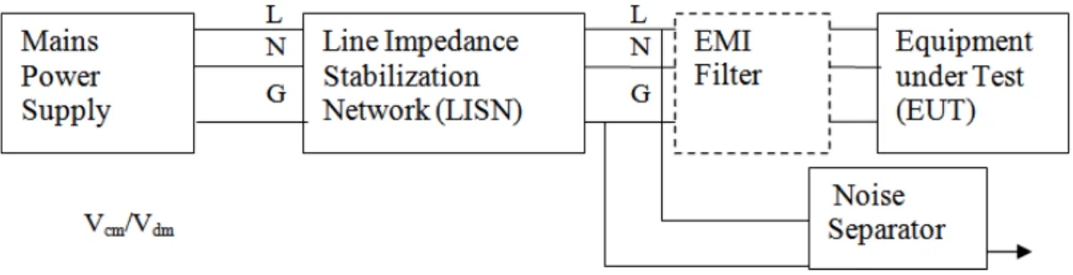
The basic setup shown in Figure2 consists of Line Impedance Stabilization Network (LISN), Equipment under Test (EUT) which is a 2-transistor SMPS circuit, mains power supply and a noise separator circuit
Figure 2: Conducted emissions measurement setup
Line Impedance Stabilization Network (LISN)
The conducted EMI measurement procedure requires a 50 W/ 50 mH Line Impedance Stabilization Network (LISN) to be inserted between the equipment under test (EUT) and the ac utility line to provide specified measuring impedance for noise voltage measurement [5]. The basic schematic of LISN is shown in Figure3.
Euipment Under Test (E The EUT used in this s transistors, diodes which generated.
Noise Separators
The common mode and separated using a noise se while an active circuit is u Basic EMI filters
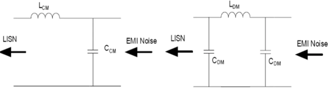
There are numerous EMI most popularly used are th respectively [13]. The aim the filter and the outside sy
Figure 4: Ind
Figure 3: Schematic of LISN.
EUT)
setup is a 2-transistor SMPS circuit that c h act as noise sources from which cond
differential mode noises from the measu eparator. DM noise rejection is done using a used for CM noise rejection.
filters that could be considered for noise red he LC inductor filter and the π filter for CM m is to obtain the maximum impedance mis
ystem.
ductor filter Figure 5: π fil
consists of two ducted EMI is
ured output are a passive circuit
duction, but the and DM noises smatch between
A better solution over the inductor filter is the choke filter. Chokes withstand high DC currents without degradation of filtering performance. Chokes reduce noise considerably over the entire desired frequency range.The components of inductor filter are designed such that
If P CM Z C w(2 ) << 1 , then Ω >>25 ) (LCM w (3)
Where LCM and CCM are inductor and capacitor used in the design of inductor filter and ZP is the impedance of the euipment used [3].
The components of π filter are designed such that
If 100 ) ( 1 >> DM C w and P DM Z C w( ) << 1 , then Ω >>100 ) (LDM w (4)
Where LDM and CDM are inductor and capacitors used in the design of π filter and ZP is the impedance of the equipment used [3].
Conducted Emissions Measurements
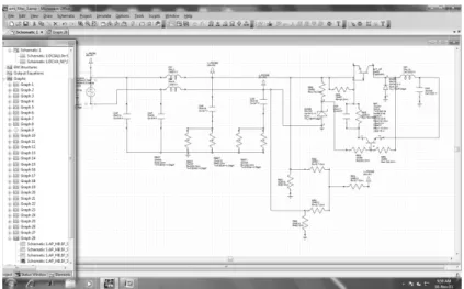
The experiment was initially conducted with the measurement setup shown in Figure2, but without filter across 150KHz-1.5MHz frequency range. The actual connected schematic has been shown in Figure6. The measured common-mode noise voltage, Vcm (dB) and DM noise Vdm (dB) across the noise separator, are shown in Figure7 and Figure8. Using these magnitudes, the insertion loss graphs were obtained in MATLAB. The simulation plots obtained in MATLAB showed that the VcmdBµV and VdmdBµV without filter have exceeded the VlimdBµV set by the EMC standard for Class B equipment. Hence, the basic EMI filters were designed to be placed between the LISN and EUT and the noise outputs were once again measured and graphs were simulated.
Figure 6: Conducted em
Figure 7: Vcm(dB) m
Figure 8: Vdm(dB) m
missions measurement setup using AWR-Micr
measured without filter across output of noise
measured without filter across output of noise
rowave Office.
separator.
The Insertion loss without filter was calculated by, dBuv dBuV cm dBuv cm
V
V
IL
=
−
lim (5) dBuv dBuV dm dBuv dmV
V
IL
=
−
lim (6)where, Vcm is the common mode noise obtained in Microwave office whose magnitude is shown in Figure7, Vdm is the value differential mode noise obtained whose magnitude is shown in Figure8. Vlim is the EMC limit for conducted emissions which is in dBμV and hence the output noise obtained is converted into dBμV by adding 120 to output noise magnitude[5]. The aim was to design the filter to reduce the CM and DM noises and hence the design needs an insertion loss greater than that given equations 5 and 6.
Hence, the filter components were tuned in Microwave Office refereing to the equations 3 and 4 such that they produce noise voltages that would give an Insertion loss greater than that in equations 5 and 6. Once these components were tuned to give the required insertion loss, the same was simulated in MATLAB using the equations 7 and 8 for inductor and π filter for CM and DM noises respectively. The obtained insertion losses using the filters is simulated using,
dBuv cmif dBuV cm dBuv cmif V V IL = − (7) dBuv dmif dBuV dm dBuv dmif V V IL = − (8)
where, VcmdBμV and VdmdBμV are values obtained without using filter and Vcmif and Vdmif are the noise voltages obtained after tuning filter components for inductor and π filter respectively.
Inductor filter
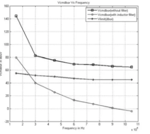
The inductor filter was placed between the LISN and EUT and the filter circuit was tuned to obtain insertion loss greater than the loss obtained before embeding filter across the desired frequency range. The obtained CM noise voltage, VcmifdB was measured across the output of noise separator in AWR-Microwave Office. It could be observed that noise output reduced considerably by using the inductor filter. Figure9(a) shows that for frequencies from 300KHz-1.5MHz, the noise is within the limits specified by EMC standards. To obtain desired insertion loss below 300KHz, the choke filter was used instead of inductor filter and the results were obtained as in Figure9(b).
Choke filter
It shows that by using choke filter there is a tremendous reduction in noise for frequencies less than 300KHz and over the entire range till 1.5MHz. The loss simulations are shown in Figure10.
Figure 9(a): Comparision standards
Figure 9(b): Comparision by EMI standards
Figure 10: Insertion los comparison to insertion lo
.
n of CM Voltage with and without filter with V
n of CM voltage without filter and with chok
ss(dBuV) vs Frequency for inductor and oss without filter.
Vlim set by EMI
ke with Vlim set
Figure 11: Comparison o standards.
Figure 12: Insertion loss( loss without filter.
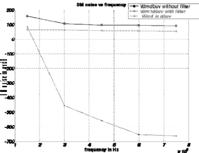
pi filter
To reduce the differential EUT and the filter was obtained is greater than th range. The result obtaine measurement with and wit
Results
The conducted emissions loss of around 40-90dBμV
of DM output with and without filter with V
(dBµV) vs Frequency for filter in compari
-mode noise, the filter was placed between tuned to obtain DM noise voltage, whose he loss before embeding filter across the des ed is shown in Figure11. Figure12 plots the
thout π filter
measurement setup without the filter produc V for 150-300KHz frequency range and 30
Vlim set by EMC
son to insertion
n the LISN and e insertion loss
sired frequency e insertion loss
ced an insertion 0dBμV over the
Conclusion
The inductor filter produced desired insertion loss for frequencies from 300KHz-1.5MHz, but the choke filter produced better results than the inductor filter and also the obtained noise reduced considerably over the entire considered frequency range from 150KHz-1.5MHz. The π filter is a good option for reducing the DM noise over the frequencies from 150KHz-750KHz. Hence, choke and pi filter are good EMI solutions over the conducted emissions range of 150KHz-1.5MHz.
References
[1] Klaus Raggl, Thomas Nussbaumer, Johann W. Kolar “Guideline for a Simplified Differential-Mode EMI Filter Design” IEEE TRANSACTIONS ON INDUSTRIAL ELECTRONICS, VOL. 57, NO. 3 MARCH 2010.
[2] P. Ram Mohan, M. Vijaya Kumar, O .V. Raghava Reddy, ”a novel topology of EMI filter to suppress common mode and differential mode noises of electromagnetic interference in switching mode power supplies”, VOL. 2, NO. 4, AUGUST 2007 ISSN 1819-6608 ARPN Journal of Engineering and Applied Sciences.
[3] Jukka-Pekka Sjöroos “Conducted EMI filter design for SMPS”, Helsinki University of Technology, Power Electronics Laboratory.
[4] EMC Lab Info: www.emclabinfo.com.
[5] Richard Lee Ozenbaugh, 2001, ’EMI Filter Design’.
[6] Maria Carmela Di Piazza, Member, IEEE, Antonella Ragusa, Member, IEEE,
and Gianpaolo Vitale, Member, IEEE, ”Design of Grid-Side Electromagnetic
Interference Filters in AC Motor Drives With Motor-Side Common Mode Active Compensation”, IEEE TRANSACTIONS ON ELECTROMAGNETIC COMPATIBILITY, VOL. 51, NO. 3, AUGUST 2009.
[7] Mel Berman, October 2008, ”All about EMI filters”, www.us.tdk-lambda.com. [8] IMPACT - module 5, ”conducted EMI/EMC”, Indian institute of technology,
new Delhi
[9] M. L. Heldwein, T. Nussbaumer; and J. W. Kolar, ”Differential Mode EMC Input Filter Design forThree-Phase AC-DC-AC Sparse Matrix PWM
Converters”, Swiss Federal Institute of Technology (ETH) Zurich, Power Electronic Systems Laboratory, ETH Zentrum / ETL H23, Physikstrasse 3, CH-8092 Zurich, SWITZERLAND.
[10] , ”Limits and methods of measurement”, Information technology equipment - Radio disturbance characteristics, 1998.
[11] CISPR16 specialization for radio interference and immunity measuring apparatus and methods, Int. Electrotech. Comm., Geneva, Switzerland, Nov. 2003.
[12] CISPR 22, Information Technology Equipment—Radio Disturbance Characteristics—Limits and Methods of Measurement, Int. Electrotech.Comm., Nov. 1997.
[13] Vuttipon Tarateeraseth, Student Member, IEEE, Kye Yak See, Senior Member, IEEE, Flavio G.Canavero, Fellow, IEEE, and Richard Weng-Yew Chang, Member, IEEE, ” Systematic Electromagnetic Interference Filter Design Based
on Information From In-Circuit Impedance Measurements”, IEEE TRANSACTIONS ON ELECTROMAGNETIC COMPATIBILITY, VOL.52NO.3, August2010.