BEYOND
A Dissertation Submitted to the Faculty
of
Purdue University by
Xufeng Wang
In Partial Fulfillment of the Requirements for the Degree
of
Master of Science in Electrical and Computer Engineering
May 2010 Purdue University West Lafayette, Indiana
ACKNOWLEDGMENTS
I would like to express my sincere thanks to both my advisors, Professor Gerhard Klimeck and Professor Mark Lundstrom for their guidance and help throughout my Master study here at Purdue. I met Professor Klimeck four years ago when I was an undergraduate student. It was him who first brought me into the realm of nanoelec-tronic research. He provided me with opportunities and support in various projects, and more importantly the freedom to explore and guidance when needed. For ev-erything he has done for me, I’m forever indebted to him. I equally thank Professor Lundstrom for his kindness to take me under his guidance as well. He is always very careful in studies and pays attention to details, which sets out great examples for me. I especially liked his strict ”understanding before doing” attitude, and benefited much from his experience and knowledge.
I’m also very thankful for all the helps I’ve received from discussion with Dr. Mathieu Luisier, Dr. Tillmann Kubis, Dr. Sebastian Steiger, Dr. Tony Low, and other post doctoral fellows. Whenever I run into a problem and bother them, they’ve always been kind and patient to answer me. I especially thank Dr. Tillmann Kubis for reading my thesis and recommendations and help on LaTeX issues.
I appreciate the help and support from my colleagues here at NCN@Purdue, especially my peers from Professor Klimeck’s and Professor Lundstrom’s research groups. I thank Yunfei, Yang, Himadri, Dionisis, Zhengping and many others for the fruitful discussions.
Mrs. Cheryl Haines and Mrs. Vicki Johnson has my many thanks for helping me over various scheduling and tasks. They are the most dutiful secretaries I’ve every seen.
Outside of Purdue, I would like to thank Dr. Dmitri Nikonov for guidance on nanoMOS development and reading my thesis. Dr. Nikonov is a knowledgeable
pro-fessional from industry, and I particular liked his visits since he always had nice stories and refreshing prospectives. I also thank Professor Dragica Vasileska at University of Arizona for her help over various topics over the past several years.
I would also like to thanks Professor Alejandro Strachan for serving on my advisory committee.
This August marks the 6th anniversary of my day at Purdue. Life here is quiet and wonderful, and everyday of mine is delighted by all the friends I have around. D.C. trip with Zhengping and Yi, Chicago visit with Yunfei, cherry picking with Yang...little pieces here and there forms the unforgettable memory which deepens my love for this place. To all my dear friends: I’m just so glad to have you!
Last but the most, I would like to thank my entire family for their support and love. No word can describe how much I love and miss them. I’m also fortunate enough to have the best girl on earth, Hui to care for me. For all of this and to all of them, I dedicate my work.
TABLE OF CONTENTS
Page
LIST OF FIGURES . . . vi
ABSTRACT . . . x
1 Introduction . . . 1
1.1 Difficulties in Si MOSFET scaling . . . 1
1.2 Emerging candidates for Si transistor replacement . . . 3
1.2.1 Si Double-gated MOSFET . . . 3
1.2.2 III-V Double-gated MOSFET . . . 5
1.2.3 Schottky barrier FET. . . 5
1.2.4 III-V High Electron Mobility Transistor (HEMT) . . . 6
1.2.5 SpinFET. . . 7
1.3 Development history . . . 9
1.4 Objective . . . 11
1.5 Chapters overview . . . 12
2 Semi-classical transport in nanoMOS . . . 14
2.1 Introduction . . . 14
2.2 Transport model overview . . . 15
2.3 Overall scheme of nanoMOS simulator . . . 16
2.3.1 Introduction . . . 16
2.3.2 Basic equations . . . 16
2.3.3 Self-consistent calculation . . . 18
2.3.4 Effective mass model . . . 19
2.3.5 Mode space approach . . . 20
2.4 Drift-diffusion transport . . . 22
Page
2.4.2 Equation reformulated . . . 24
2.4.3 Scharfetter and Gummel Method . . . 27
2.4.4 Drift-diffusion current . . . 32
2.5 Semi-classical Ballistic transport . . . 33
2.5.1 Introduction . . . 33
2.5.2 The top of the barrier model . . . 33
2.5.3 Electron density in top of the barrier model . . . 34
2.5.4 Ballistic current . . . 38
2.6 Poisson’s equation . . . 41
2.6.1 Introduction . . . 41
2.6.2 Device grid and boundary conditions . . . 42
2.6.3 Transport-Poisson coupling with Gummel scheme . . . 47
2.6.4 Transforming electron density between 2D and 1D . . . 47
2.6.5 Coupled solution scheme . . . 49
2.6.6 Non-linear damping. . . 50
2.6.7 Newton-Raphson iteration for Poisson’s equation . . . 52
3 Quantum ballistic transport . . . 58
3.1 Introduction . . . 58
3.2 Transport model overview . . . 59
3.3 System Hamiltonian . . . 59
3.3.1 Introduction . . . 59
3.3.2 The Schrdinger equation . . . 60
3.3.3 Choice of basis: atomistic tight-binding vs. effective mass model 61 3.3.4 Choice of representation: real space vs. mode space . . . 65
3.3.5 System Hamiltonian in matrix form with finite difference ap-proximation . . . 69
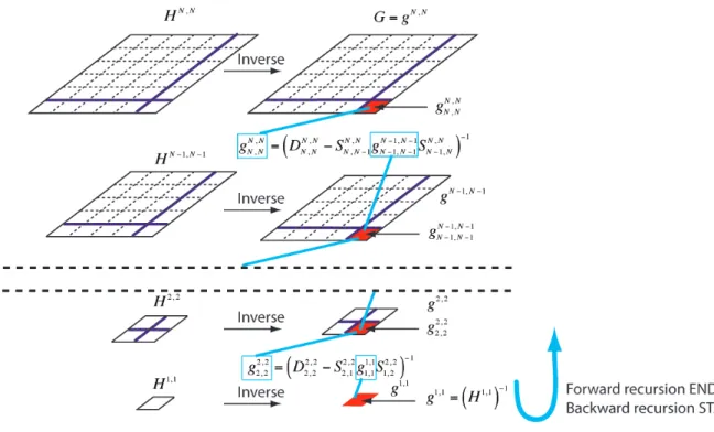
3.4 Recursive Green’s Function formalism. . . 72
Page
3.4.2 Motivation. . . 72
3.4.3 Dyson’s equation and recursive method . . . 74
3.5 Simple NEGF formalism . . . 84
3.5.1 Introduction . . . 84
3.5.2 Ballistic NEGF electron density . . . 84
3.5.3 Ballistic NEGF current . . . 86
4 nanoMOS 4.0 Application Example . . . 89
4.1 Introduction . . . 89
4.2 Model Device: an Undoped-body Extremely Thin SOI MOSFET with Back Gate . . . 90
4.3 Results: Internal Quantities . . . 92
4.3.1 Introduction . . . 92
4.3.2 Internal Quantities . . . 92
4.4 Results: IV Characteristics . . . 104
4.4.1 Introduction . . . 104
4.4.2 I-V characteristics in the ballistic limit via NEGF . . . 104
4.4.3 Subthreshold characteristics . . . 106
4.5 Results: Comparison between various transport models . . . 110
4.5.1 Semiclassical Ballistic vs. Quantum Ballistic . . . 110
4.5.2 Drift-Diffusion vs. Quantum Ballistic . . . 113
4.6 Summary . . . 115
5 Auxiliary programs of nanoMOS. . . 117
5.1 Introduction . . . 117
5.2 Graphical User Interface . . . 117
5.2.1 Introduction . . . 117
5.2.2 Rapid Application Infrastructure (Rappture) toolbox . . . . 118
5.2.3 Understanding the Rappture toolbox . . . 119
Page
5.3 nanoMOS on computer clusters . . . 123
5.3.1 ”Embarrassingly parallel” scheme . . . 123
5.3.2 nanoMOS Parallel Job Submitter (PJS) . . . 125
5.4 Benchmark and testing suite . . . 125
A Finite difference method (FDM) and discretization of Hamiltonian . . . . 127
B Matrix inversion techniques . . . 128
B.1 Matrix types . . . 128
B.2 LU Decomposition . . . 129
C Bandstructure calculation, wavefunction and NEGF formalism in atomistic tight-binding simulation . . . 130
C.1 Introduction . . . 130
C.2 Complex electronic bandstructure . . . 130
C.3 Wave function formalism . . . 134
C.3.1 Alternative form . . . 139
C.3.2 Choice ofk . . . 141
C.3.3 Transmission from coefficient . . . 143
C.4 NEGF formalism . . . 144
C.4.1 Contact Self-energy from wavefunction formalism . . . 144
C.4.2 Other methods of determining contact self-energy . . . 145
LIST OF FIGURES
Figure Page
1.1 Ideal double-gated MOSFET structure used in nanoMOS. Source, drain, and channel are all of same semiconductor material. . . 3 1.2 Ideal Schottky barrier FET structure used in nanoMOS. It’s similar to
double gate MOSFET except with metallic contacts. . . 5 1.3 Ideal HEMT structure used in nanoMOS. . . 6 1.4 Ideal spinFet structure used in nanoMOS. Here we show an example of
up-spin electrons being transported across the channel. In this case, the two HMF layers are in parallel configuration. Size of dot denotes relative population of electrons with that spin. . . 8 2.1 Picture shows the change in point of view from an electron with rest mass
traveling in crystal lattice to one with modified mass traveling in constant potential. By introducing the so called ”effective mass”, we eliminate the need to consider the rapid changing potential from crystal lattice and simplified our calculation. . . 19 2.2 1D Schrdinger equation is solved in each vertical slice illustrated in the
figure. The grid is same as the one used in Poisson’s solver. . . 21 2.3 Comparison between wavefunction profile bewteen oxide penetration on
and off. . . 22 2.4 It shows a possible trajectory of an electron traveling in diffusive manner
across the channel. Red crosses are scattering centers where electron’s momentum is relaxed. Notice electrons with energy lower than the barrier can still get across due to scattering possibly from phonon. . . 23 2.5 Illustration of the meaning of mid-nodes. The red nodes are actual solution
nodes of Poisson grid. Green nodes are midnodes which are in the middle of actual solution nodes. . . 26 2.6 Illustration of electrons injected into the channel with higher or lower
energy than top of barrier. . . 34 2.7 Illustration of electron density evaluation at point A (red box on the left).
The red box includes every possible electron ”stream”, and resulting elec-tron density is just a simple summation of all the streams. . . 35
Figure Page 2.8 Illustration of electron current calculation at point A (red box on the left). 39 2.9 The device grid and boundary conditions used for solving Poisson’s
equa-tion. The actual grid is finer than the one illustrated here. . . 42 2.10 Illustration of Control Volumn Method (CVM) on nodeφm,n. The dashed
black box is the control volumn . . . 44 2.11 This chart illustrates how to convert electron density between 2D and 1D
within a certain vertical slice. . . 48 2.12 Illustration of how Newton iterations converge toward a solution with a
good starting guess. . . 53 2.13 Illustration of Newton iteration with a bad starting guess can be saved
from divergence with Brown and Lindsay suggested fix. . . 56 3.1 Forward partition of total Hamiltonian. The lower right piece is just the
Hamiltonian of a single layer. The two non-square pieces are the coupling between the singled out layer and rest of the device. . . 78 3.2 Illustration of recursive partition of Hamiltonian matrix and the chain of
equations associated with it. . . 80 3.3 After the first recursion process, we forward partition again to obtain the
diagonal and nearest off-diagonal blocks. This time however, we partition the blocks differently. . . 82 3.4 Illustration of the second forward partition process. The red blocks are
ones determined, and green blocks are ones to be determined in that re-cursion step. . . 83 4.1 Fabricated device structure by IBM Corporation. The curve cut in buried
oxide layer indicates a thick region not shown in the figure. The nanoMOS simulation region is enclosed by the dashed line. . . 90 4.2 Electrostatic potential profile of entire device region. Most of the plot is
occupied by the buried oxide layer which is 145nm thick. . . 93 4.3 Electrostatic potential profile focusing on channel region. ”x” is transport
direction; ”z” is transverse direction. . . 93 4.4 Bottom conduction band profile in the transverse direction. . . 94 4.5 Electron density distribution of entire device. Majority of the plot is void
Figure Page 4.6 Electron density distribution focusing on channel region. Due to quantum
confinement in transverse direction, the electron density exhibit wave-like pattern in source and drain. Electron density in channel is low compared to those in the source and drain, so it is difficult to observe in this plot. 96 4.7 Electron density distribution in transport direction. Notice the log scale
of this plot. . . 96
4.8 Average carrier velocity along the channel. . . 97
4.9 Energy vs. transmission coefficient. 0eV reference is the quasi-Fermi level in source, where electrons are injected from. . . 98
4.10 LDOS induced by the source . . . 100
4.11 LDOS induced by drain. . . 100
4.12 Full LDOS induced by both source and drain. . . 101
4.13 Energy resolved current density. The white curve is a line illustration of current density vs. energy. . . 102
4.14 Energy resolved current density foucsing around quasi-Fermi level at source 102 4.15 Energy resolved electron density. . . 103
4.16 Id vs. Vg with various back biases.. . . 105
4.17 Electrostatic potential profile at back gate voltage = 0V . . . 106
4.18 Subband electron density in transverse direction at back gate voltage = 0V . . . 106
4.19 Electrostatic potential profile at back gate voltage = -20V. . . 107
4.20 Subband electron density at back gate voltage = -20V. . . 107
4.21 Threshold voltage vs. gate length at linear/saturated current with/without back gate bias. . . 108
4.22 DIBL vs. gate length, with and without back gate bias. . . 109
4.23 Id vs. Vg comparison between semiclassical and ballistic transport models in linear scale. . . 110
4.24 Id vs. Vg comparison between semiclassical and quantum ballistic trans-port models in log scale. . . 111
4.25 Conduction band profile along the channel. Zoomed into the beginning of the channel for better comparison. . . 111
Figure Page 4.26 Charge comparison between semiclassical and quantum ballistic models.
Notice the log scale in y-axis. . . 113 4.27 Average carrier velocity comparison within the channel. Two gate
volt-ages corresponding to on-state and off-state are plotted for each transport model. . . 114 4.28 Id vs. Vg comparison between drift-diffusion and quantum ballistic
trans-port models. . . 114 4.29 Charge distribution comparison along the channel. Notice the log scaled
used in y-axis . . . 115 5.1 Snapshots of nanoMOS GUI built from Rappture toolbox. It is deploied
on nanoHUB.org at https://nanohub.org/tools/nanomos. The left figure is input interface, and right one is output interface displaying a 3D plot. 118 5.2 Implementation flow chart of Rappture toolbox to nanoMOS. The red box
indicates the computational code is hidden from users. All users see and need is an easy to use graphical interface. . . 123
ABSTRACT
Wang, Xufeng MSECE, Purdue University, May 2010. NanoMOS 4.0: A Tool to Explore Ultimate Si Transistors and Beyond. Major Professors: Gerhard Klimeck, Mark Lundstrom.
This thesis discusses the modeling of nano-scale field-effect transistors using nanoMOS 4.0. Our goal is to present the reader with a comprehensive documentation of nanoMOS 4.0 including its code structure in detail, development history, and new features. As silicon device scaling is reaching its limit, nanoMOS 4.0 is able to simu-late the ultimate Si transistor performance and explore new non-silicon based devices. In this report, we focus on a simple double-gate thin-body structure for demonstration purposes. One primary aim is to show how theories are incorporated computation-ally into a fully functional simulator. Physiccomputation-ally, two main transport modules of nanoMOS, semi-classical (drift-diffusion and ballistic) and NEGF, are examined in detail including the driving theories behind them; computationally, we further dis-cuss several important numerical issues and document ”tricks of the trade” used in nanoMOS to resolve those issues. We present auxiliary programs such as a bench-mark and testing suite and discuss how they are used to support the development of nanoMOS. In the end, we demonstrate the application of nanoMOS to real devices fabricated by the Intel Corporation to illustrate the methods used to benchmark sim-ulation results against experimental data. Thus, with this report, we deliver a deeper understanding and comprehensive review of this tool to its user.
1. INTRODUCTION
The backbone of today’s digital products is the complementary metal-oxide semicon-ductor (CMOS) technology. Made from a complementary pair of p-type and n-type metal-oxide semiconductor field effect transistors (MOSFET), mass CMOS units can be cascaded, the central processing unit (CPU) within a computer for example, to carry out complicated logical computations. Since the advent of MOS transistors in Bell laboratory [1], semiconductor industry enjoyed an era of rapid growth and invented numerous revolutionary digital products that changed our lives.
One major force that pushes the advancement of digital technology so rapidly over the past several decades is the dramatic increases of CMOS speed, and such speed gain is mainly obtained by the way of MOSFET scaling–that is to make them smaller and smaller by scaling their size down proportionally (see, for example, scaling theory of Dennard [2]). MOSFET scaling enhances speed in two aspects: first of all, with its channel shortened, electrons can take less time traveling from source to drain giving it a faster switching time. Electrons in this case also encounter less scatters such as impurity and surface roughness in a shorter channel and thus gain a higher mobility. Second of all, scaling allows more devices to be packed within a certain area, making same sized CPUs more powerful and feature rich. It is desirable to have a smaller packing area, so communications between transistors would be faster. Depending on the design of the CPU, the packing area related to communication delay and devices per area related to logic power need to reach an optimized balance.
1.1 Difficulties in Si MOSFET scaling
One serious challenge is the short channel effects [3]. As the channel length being shortened, the source and drain are brought close to each other. When a barrier is induced by the gate within the channel, the barrier height has to drop to the same potential as drain on the drain side. Channel are not doped as heavily as contacts, so the screening length can be significant comparing to the channel length in nanoscale transistors, which means this lowering of barrier on the drain side occurs gradually in a significant region of the channel. In the worst case, drain may even affect the top of the barrier height in so called ”drain induced barrier lowering” (DIBL). Such undesired short channel effects weakens the control of gate and increases off-state current. In order to counter such effects, stronger gate control is needed. One solution is to have a material with high dielectric constant as the gate oxide layer so one can decrease the physical thickness of the layer and obtain a higher capacitance while retaining low gate leakage.
Besides all the physical difficulties mentioned above, another major road block in device scaling is the engineering fabrication technique being inadequate. The backbone of MOSFET fabrication is a process called lithography [4]. A pre-defined mask is first placed over a layer of deposited photoresist, and after being exposed to light, areas of photoresist not protected by mask will react and be etched off to create desired patterns. With such process repeated over and over, one can create complex layers of MOSFETs and interconnect structures. As devices being shrunk toward nanoscale today, one needs to define very fine patterns. In this case, mask alignment becomes increasingly difficult. Etching a thin channel also becomes sensitive and requires stricter control. Diffraction due to wave nature of light adds additional burden by blurring the masked edges. Although more sophisticated techniques such as electron beam lithography is able to define sharper edges, its use in mass production is not yet realized.
1.2 Emerging candidates for Si transistor replacement
Facing the many challenges of Si transistor scaling, people begin to look other ways and seek candidates to replace or complement the existing Si transistors. Many promising proposals are made, and they all have their own advantage and disadvan-tages. Modeling thus has become essential in order to understand these new devices’ behaviors and evaluate their performances.
In this thesis, we present nanoMOS [5]: a 2-D simulator for thin body (less than 5nm), fully depleted, double-gated n-MOSFETs. It’s a simple and effective program coupling Poisson’s equation with one of several transport models self-consistently. Originally designed for simulating Si n-MOSFETs, its features have been greatly expanded to model new devices by a team of developers. As of current version, nanoMOS 4.0 incorporates the following device geometries:
1.2.1 Si Double-gated MOSFET
Fig. 1.1. Ideal double-gated MOSFET structure used in nanoMOS. Source, drain, and channel are all of same semiconductor material.
Traditional bulk MOSFET is built upon a substrate of intrinsic silicon, and such MOSFET only has a single gate on the top to control the potential barrier induced in channel. As devices being scaled down, one major drawback is the loss of decent gate control due to short channel effects. A better gate controlled potential barrier
allows the MOSFET to have better current on/off ratio and substreshold slope. One way to archive this is to have two gates built symmetrically on top and bottom of the channel in the so-called double-gate MOSFET structure (Fig. 1.1).
One major difference between a traditional bulk MOSFET and double-gate MOS-FET is how electrons are confined in the channel. In a traditional bulk MOSMOS-FET, electrons traveling in the channel are confined within a triangular quantum well due to substrate band bending induced by the gate. This triangular well is located right at the semiconductor-oxide interface, so the interface roughness scatters electron trav-eling toward drain and thus degrade the mobility. In the double-gate MOSFET structure, the channel is confined by the gates to form a rectangular quantum well, and two situations may occur depending on the thickness of channel. If channel is thick, depletion simply occurs near the semiconductor-oxide interfaces, leaving mid-dle of the channel between two gates un-depleted. Thus, two separate channels are created. In addition, this also results in separations between energy levels in the well being comparable to thermal voltagekBT, electrons injected from source may occupy
several of these subbands. The resulting situation is similar to two bulk MOSFETs built back-to-back [6].
On the other hand, if the channel is thin enough (less than 5nm for example), the splitting between energy levels become significantly larger than thermal voltage, and electrons are only able to occupy the bottom subband alone without hopping to higher levels. In this case, electron spatial distribution can be obtained from wavefunction solution of Schrdinger equation, which indicates electrons are now confined within the middle of the channel. Channel is fully depleted, and mobility degradation due to surface roughness is lessoned since electrons are now concentrated away from interface. Roughly as much as 4 times the on-current has been estimated in such thin-body double-gate MOSFET than a traditional bulk structure [7].
1.2.2 III-V Double-gated MOSFET
It’s well known that electrons in III-V compound materials such as GaAs has a higher intrinsic mobility than ones in silicon. Higher mobility can be translated to much desired faster switching time and higher current density.
Based on the already discussed Si thin-body double-gate MOSFET structure, we can substitute the silicon channel with a III-V compound. In reality, building a III-V MOSFET is not a simple matter of such suggested swapping. Oxide layer in silicon devices are popularly obtained by oxidations of silicon itself into SiO2. III-V compounds however cannot be oxidized this way to create an isolating barrier. Introducing an additional oxide layer over the III-V channel is also difficult since they may not attach well to each other [4]. Alternatively, people have found structure to overcome the fabrication difficulties and utilize intrinsic III-V material as channel in device called High Electron Mobility Transistor (HEMT).
In nanoMOS, we simply assume the oxide layer is some material described by a dielectric constant and adhesive well enough with the III-V channel. In addition, several mobility models are incorporated to suit different III-V materials.
1.2.3 Schottky barrier FET
Fig. 1.2. Ideal Schottky barrier FET structure used in nanoMOS. It’s similar to double gate MOSFET except with metallic contacts.
Regular MOSFET forms source and drain by heavily doping the regions with dopant. Schottky barrier FET (Fig. 1.2) instead uses metallic material as contacts. Metal is the ideal contact because they have very low resistance and abundant amount of free electrons. When metal contact forms a junction with the semiconductor chan-nel, a Schottky barrier is formed. The upside is that this junction is abrupt which is difficult to obtain by doping. Abrupt junction means narrow depletion width, which brings faster switching behavior. In addition, the abruptness allows a superior scal-ing ability. The downside is in order to be injected into the channel, electrons has to either (rarely) hop over or (mostly) tunnel through the thin Schottky barrier.
The Schottky barrier FET operates slightly differently than a MOSFET. In a MOSFET, the gate controls the height of potential barrier within the channel. In Schottky barrier FET, the Schottky barrier at metal-semiconductor interface is present no matter what gate bias is given. The gate instead controls the width of the barrier which in return modulates the transmission of electrons tunneling through [8].
1.2.4 III-V High Electron Mobility Transistor (HEMT)
Fig. 1.3. Ideal HEMT structure used in nanoMOS.
In traditional MOSFET, the channel needs to be doped to obtain free electrons in order to conduct. However, the drawback is traveling electrons in the channel scatters
at these dopant sites, and their mobility is degraded as a result. HEMT deals with this issue by having an intrinsic channel (InGaAs) and obtaining free electrons from an adjacent doped layer of different high-bandgap material (InAlAs barrier). Due to its higher bandgap, the electrons from InAlAs spill over into InGaAs channel leaving InAlAs depleted. This creates a triangular quantum well inside InGaAs at InAlAs-InGaAs interface. Electrons in the channel are confined within this well and travel inside an intrinsic material with high mobility–notice that this resulting higher mobility is contributed by the absence of impurity scattering and inherit property for being III-V material. It’s common practice to add a heavily doped delta layer inside InAlAs. By adjusting doping dose in this delta layer, one can accurately change the threshold voltage of the HEMT.
In nanoMOS, we do not simulate the entire HEMT structure due to complications arisen from contacts. We instead only simulate the channel region where current flows horizontally in 1D manner (Fig. 1.3); inclusion of contacts will force us to consider vertical flow of current which isn’t compatible with the 1D transport models used in nanoMOS. HEMT contacts consist of layers of materials, and to take the contact into effect, we simply add a series resistance term which can be determined by fitting experimental data [9].
1.2.5 SpinFET
In addition to the gate induced potential barrier in the channel, the spin polariza-tion of electrons is able to give another degree of freedom for current control. Figure 1.4 shows one of the possible scheme for utilizing spin effects in a FET structure. This scheme is originally suggested by Sugahara and Tanaka [10], and nanoMOS simulates it with some slight modifications.
In this structure, electrons injected from a nonmagnetic source are unpolarized meaning there is equal probability for them to be up-spin or down-spin. When go-ing through a Half-Metallic-Ferromagnet (HMF), electrons become polarized in one
Fig. 1.4. Ideal spinFet structure used in nanoMOS. Here we show an example of up-spin electrons being transported across the channel. In this case, the two HMF layers are in parallel configuration. Size of dot denotes relative population of electrons with that spin.
spin direction (up-spin or down-spin). HMF is able to effectively polarize electrons to about 100%. Magnetization of the HMF layer determines the polarization direc-tion of the electron, and it can be switched, for example, by spin transfer torque of the flowing current through. The HMF layer and semiconducting channel (silicon in this case) forms a Schottky barrier which the polarized electrons tunnel through. The gate, just as in the case of Schottky barrier FET, modules the thickness of the Schottky barrier and attenuates the transmission probability of the electrons. On the drain side of the channel, polarized electrons encounter a second layer of HMF, which may or may not have the same magnetization with the first. In case of same mag-netization, or the so called parallel configuration, the polarized electrons can simply travel through and reach the nonmagnetic drain; in case of opposite magnetization, or anti-parallel configuration, the polarized electrons cannot travel through the second HMF layer, and the resulting current is greatly lessoned. Therefore, both the gate and magnetization of HMF layers have impact on the current.
The theoretical operation of Sugahara-Tanaka spinFET we just described ignores several experimentally observed factors. First of all, it is suggested that the po-larization of electrons is randomized to a certain degree at HMF and semiconductor interface. This randomization, of course, is not 100% which would render the spinFET
pointless, but its effect is significant enough to be necessarily considered. Therefore, for the sake of modeling in nanoMOS, an additional artificial layer of ”randomiza-tion layer” is added between the HMF and semiconducting channel. Within this ”randomization layer”, spin are randomly flipped with a pre-set probability.
Another issue is the conduction mismatch between the HMF and semiconductor. Due to randomized polarization, both up-spin and down-spin electrons enter channel, but the existence of conduction mismatch undesirably causes the population difference between them to decrease. To lesson this effect, an additional thin oxide layer is placed between randomization layer and semiconductor channel. Both population of up-spin and down-spin are reduced by this oxide tunneling layer, so their difference remains roughly the same after entering the channel.
In nanoMOS, the spin relaxation of electrons in channel is also considered. This, however, is implemented numerically by concept of self-energy in NEGF calculation [11].
1.3 Development history
• nanoMOS 1.0 (Published in 2000) Developer: Zhibin Ren
Original nanoMOS code for silicon MOSFETs is written in MATLAB. • nanoMOS 2.0 (Published in 2005)
Developer: Steve Clark, Shaikh S. Ahmed
Rappture interface is added to nanoMOS, and the code becomes avaliable on nanoHUB.org.
• nanoMOS 3.0 (Published in 2007) Developer: Kurtis Cantley
Support for III-V materials in semi-classical ballistic and quantum ballistic transport models is added. Rappture interface is updated to reflect the III-V implementation.
• nanoMOS 3.0 (Published in 2007) Developer: Himadri Pal
Top and bottom gate can now have asymmetric configurations with different gate dielectrics and capping layers.
• nanoMOS 3.5 (Published in 2008) Developer: Xufeng Wang
Support for III-V materials in drift-diffusion transport is added. Additional mobilities models are added.
• nanoMOS 3.5 (Published in 2009)
Developer: Xufeng Wang, Dmitri Nikonov
nanoMOS source code is restructured and modularized. Material parameters are separated out as a mini-library. Debugging functions are planted within source code to assist code developments. Benchmark and testing suite is created based on a script from Dmitri Nikonov.
• nanoMOS 4.0 (Developed in 2009) Developer: Himadri Pal
Support for Schottky FET is added. NanoMOS now has the ability to simu-late a double gate MOSFETs structure with metallic source/drain via NEGF formalism.
• nanoMOS 4.0 (Developed in 2009) Developer: Yang Liu
Support for HEMT is added. NanoMOS now has the ability to simulate a III-V HEMT structure via NEGF formalism.
• nanoMOS 4.0 (Developed in 2009) Developer: Xufeng Wang
Parallel Jobs Submitter (PJS) is added. PJS allows nanoMOS to sweep gate/source bias and run each bias on a cluster node. It supports only clusters with Portable Batch System (PBS) installed such at steele (steele.rcac.purdue.edu) or coates (coates.rcac.purdue.edu).
• nanoMOS 4.0 (Developed in 2009) Developer: Yunfei Gao
Support for SpinFET is added. NanoMOS now has the ability to simulate a SpinFET structure via NEGF formalism.
• nanoMOS 4.0 (To be published in 2010) Developer: Xufeng Wang
Merge working branches of Schottky FET, HEMT, and SpinFET modules. Code is restructrued. Rappture interface is updated to accommodate the newly published features.
1.4 Objective
This thesis is dedicated to a comprehensive documentation of nanoMOS simula-tor at its latest version 4.0. Since its creation in 2000, nanoMOS has expanded from a simple Si MOSFET simulator to one that is rich in feature with several transport models and device types incorporated. Like any other simulation program, it is essen-tial to look through the user interface and understand the physics buried underneath; using a program without sufficient knowledge and understanding of its internal struc-ture like a magical black box is no different than seeking an answer from a crystal
ball, and data it spills out will offer no insight whatsoever. As the program grows to be more complex, it is also important to keep tracks of the changes and document the progress. Auxiliary programs are written to wrap around the core to provide au-tomatic services such as data plotting, parallel submission, and benchmarking. Thus, in this thesis, we aim to boil the code down to details and discuss its meaning and origin including what physics is implemented, how it is incorporated numerically, and why it is done that way. Any interested user who has seen what nanoMOS can do will see why nanoMOS can do from this thesis.
1.5 Chapters overview
In chapter 2, we will look at the semi-classical transport models deployed in nanoMOS. NanoMOS currently has two models based on semi-classical approach: the drift-diffusion model and the top of the barrier model. 1D Drift-diffusion equation is solved in transport dimension by the merit of mode space approach, and Scharfetter and Gummel method is used to ensure stability of the solutions. The top of the barrier model is the solution to Boltzmann’s equation in its ballistic limit. Carriers having energies higher than the top of the potential barrier within the channel will be fully transmitted through. The 1D electron density obtained from these classical transport equations are then expanded to 2D grid based on solutions of Schrdinger equation in confinement direction. Electron density and electric potential has to satisfy Poisson’s equation at the same time, so a 2D Poisson’s equation is solved via controlled volume method. The coupling between Poisson’s equation and transport equation forms the self-consistent scheme which iterates until a converged solution is found.
In chapter 3, we will look at the quantum transport models deployed in nanoMOS. Quantum treatment allows us to take into account the phenomena such as interference and tunneling that are not accounted for in semi-classical pictures. These quantum phenomena has significant impacts on off-current and electron density distribution. We first open discussion with examination of effective mass model and mode space
approach. We present and validate Schrdinger equation within these approxima-tions. Effective mass Schrdinger equation is then solved via the non-equilibrium Green’s function (NEGF) formalism, and it’s coupled with Poisson’s equation for self-consistency. In this chapter, we introduce the recursive Green’s function (RGF) method as an efficient way to obtain quantities of interest such as current and electron density.
In chapter 4, we will use nanoMOS 4.0 to simulate a SOI MOSFET fabricated by IBM corporation. It is important to benchmark a simulation program with real device to verify its validity and compare the results. We overview several important internal plots obtainable in nanoMOS and discuss their meaning. The subtreshold characteristics which is essential to device design and operation can be explored with nanoMOS 4.0. We also take this opportunity to see how different transport models predicts the device performance differently.
In chapter 5, we will look at the auxiliary programs designed for nanoMOS. As nanoMOS becoming richer in feature and more popular in demand, several auxiliary programs are made to enhance the capability of nanoMOS software. A graphical user interface (GUI) has been made to allow users to communicate with nanoMOS easier. The GUI is powered by Rapid Application Infrastructure (rappture) developed by nanoHUB.org. To accommodate large parallel submissions of nanoMOS jobs on clus-ters, a parallel job submitter has been created to automate the process. Subversion is used to provide version control for software development, and in addition to ensure the wellness of the nanoMOS code in development, a benchmark module is developed to test and check for possible code breakdowns.
2. SEMI-CLASSICAL TRANSPORT IN NANOMOS
2.1 Introduction
A major branch of nanoMOS simulator is the semi-classical transport module. It consists of the diffusive transport model based on drift-diffusion equation and the ballistic transport model based on Boltzmann’s equation [12]. With the same simulation structure, this gives an opportunity for one to run both semi-classical transport models and compare the results. Implementing these equations require numerical details and tricks often omitted from result oriented literatures. Here we look into the details of how these semi-classical transport models are incorporated into nanoMOS.
We start by overviewing the characteristics of the semi-classical branch including its advantages and disadvantages comparing to quantum transport branch. We then exam some critical assumptions and concepts fundamental to the nanoMOS scheme. After establishing a common ground, the implementation of drift-diffusion transport is discussed. We show that the Scharfetter and Gummel method [13] is needed in order to insure stability of the drift-diffusion equations. For the ballistic limit counter-part, top of the barrier model [12] is illustrated and discussed as an equivalent of solution to Boltzmann’s equation in absence of scattering. The electron density output from any transport equation is then coupled with Poisson’s equation for self-consistency. We describe the implementation details of Control Volume Method (CVM) [14] and Newton-Raphson iterations used in our simple Poisson solver. In the end, some important numerical convergence issues are discussed.
2.2 Transport model overview
Our task here is to simulate how electrons move in a certain device geometry. For this, we have different choices of models to use. Each of the models is based on certain facts and assumptions, resulting in their own advantages and disadvantages.
Classically, electrons are treated as particles and their dynamics can be described by the Boltzmann equation. In case of large amount of scattering events occurring during the flight of the particle, the Boltzmann equation becomes the familiar drift-diffusion equation in the diffusive limit; on the other hand, in case of total absence of scattering, the Boltzmann equation can be directly evaluated to obtain the ballistic performance of the device in the ballistic limit [12]. Boltzmann equation however does not take into account any quantum effects such as interference and tunneling, thus it is a pure classical treatment.
However, some important aspects of electronic transport especially in case of nanoscale MOSFETs originate from quantum effects and cannot be simply ignored. In case of semi-classical transport models, we avoid the complicated full quantum treatment and instead fuse the simplicity of classical treatment with some quantum corrections. The quantum corrections are reflected in the usage of electron effective mass and the calculation of subbands in confinement direction.
Semi-classical transport models we deployed in nanoMOS thus have the great advantage of being simple and computationally efficient comparing to full quantum treatments. It of course has the disadvantage of not being able to capture some important quantum effects and thus unable to explain certain transport phenomena. In nanoMOS, two semi-classical transport models are available: drift-diffusion and semi-classical ballistic transport models.
2.3 Overall scheme of nanoMOS simulator 2.3.1 Introduction
In this section, we look at preliminary topics essential to drift-diffusion model, and some of them are also common for the rest of nanoMOS. We first present the three basic equations underlying the validity of drift-diffusion equation in its finite difference discretized form. The concepts of self-consistency, mode space approach, and effective mass are just simply pointed out without any demonstration nor derivation. These topics will be addressed in great details in chapter 3.
2.3.2 Basic equations
The underlaying principles making the simulation of electronic transport possible can be described by a system of basic equations.
Transport equations
Transport equations such as the Boltzmann equation can describe electron dy-namic. They determine the dynamics of electron density distribution in response to perturbation such as external electric field and electron density gradient. The electron drift-diffusion equation is shown as an example
Jn=qnµnξ+qDn∇n =−qnµn∇φ+qDn∇n (2.1)
Jn electron current density
n electron density µn electron mobility
Dn electron diffusion coefficient
Poisson’s equation
Poisson’s equation is a fundamental equation describing the spatial relationship between a certain electron density distribution and the corresponding electric field. It holds true no matter which transport equation/model we use, so it is a common routine for all simulation options.
∇2φ=−1 ε
�
p−n+ND+−NA−� (2.2)
φ electrical potential p, n electron, hole density
ND+, NA− donor, acceptor density
In nanoMOS, we assume the absence of holes and only treats electrons. Thus, Poisson’s equation becomes
∇2φ=−1 ε
�
−n+ND+−NA−� (2.3)
Continuity equation
The continuity equation unlike Eq. (2.1) and (2.2) deals with time-dependent phenomena such as carrier generation and recombination. Essentially it is an equation stating the conservation of current which is a fundamental property of nature.
∂n ∂t =
1
q∇J+G−R (2.4)
n electron density
J electron current density
G, R electron generation, recombination rate
In case of steady-state situation without generation nor recombination, the conti-nuity equation reduces to a simple form and states the conservation of electron current
density spatially throughout the entire device. In another word, current density is simply a constant in this particular case (constant cross-section area for current along x and constant current density along y).
∇J = 0 (2.5)
2.3.3 Self-consistent calculation
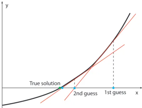
Observe the three basic equations: there are three unknowns in total, n, φ, and J. Throughout entire device, J is a constant, while the other two can vary with position. Poisson’s equation contains two unknowns, n and φ, while the transport equation contains all three; continuity equation contains a simple derivative of J which cannot be used to determine its exact value. We thus start from the Poisson’s equation as a break-in point.
Notice if electron density distributionn OR electric potentialφsomehow becomes known to us, the entire problem is then readily solved. We start the simulation by reasonably guessing an electric potential profile φ, solve transport equation for electron density distributionn,and then insertninto Poisson’s equation to backward calculate a new φnew. If φnew agrees with φold within certain tolerance, our solution
is ”converged” and our guess is good. In nanoMOS, this tolerance factor is a user defined convergence parameter. If not, we update the guess and repeat this loop until solution is converged. The uniqueness theorem for second order elliptic equation guarantee the converged solution is the only solution to the Poisson’s equation [15]. This widely used iterative scheme is called ”self-consistent calculation” or Gummel’s method [16], [17].
Of course, one can also start with an electron density distribution n guess and Poisson’s equation to initiate the self-consistent calculation. The most important message here is: no matter where you start, one has to find a pair ofn and φsatisfies all three basic equations at the same time.
2.3.4 Effective mass model
An important aspect of nanoMOS simulator is the use of effective mass model [13]. In this section, we simply point out the results and consequences of this model. A more detailed look on its derivation and validity is deferred to chapter 3.
Fig. 2.1. Picture shows the change in point of view from an electron with rest mass traveling in crystal lattice to one with modified mass traveling in constant potential. By introducing the so called ”effective mass”, we eliminate the need to consider the rapid changing potential from crystal lattice and simplified our calculation.
Electrons traveling in a crystal ”feel” the existence of the lattice structure. This microscopic detail has great impact on the electronic transport property and cannot be simply ignored. In the so-called Kronig-Penney model [18], crystal lattice is modeled after a series of finite barrier rectangular quantum wells reflecting the atomic sites and spacings in between. Such approximations are helpful to account for the crystal lattice effects, but they are not feasible computationally in our large structure containing tens of thousands atoms. In the effective mass model, we use a modified version of electron’s free mass, the effective mass [19], to collectively account for the lattice effects. Therefore, with a change of electron mass, we can ignore the lattice details and continue to use classical equations. This is the main advantage of effective mass model over others.
Effective mass can be obtained empirically from experimental studies such as cyclotron resonance [20] and direct measurement of electronic band structures [21]. In nanoMOS, we simply import effective mass parameters from widely used sources such as [22]. In general, effective mass varies mainly with material type and crystal
orientation. One needs to specifies these or lookup a proper effective mass to be used in nanoMOS simulation.
2.3.5 Mode space approach
Another important aspect of nanoMOS simulator is the use of mode space ap-proach. In this section, we simply point out the results and consequences of this approach. A more detailed look on its derivation and validity is presented in the later chapter.
nanoMOS studies a MOSFET thin channel sandwiched between two gate oxide layers. It is essentially a quantum well structure formed when the width of the well is narrow (less than 10nm), and energy separations between bound states (subbands) become several times larger than thermal energy kBT. As a result, it is proper to
assume electrons residing in different states do not interact with each other. The as-sumption of uncoupled subbands merits us to treat electrons in each state separately, instead of treating all electrons together. This ”divide and conquer” plan relieves the computational burden and is the main motivation for its usage in nanoMOS.
In order to solve for the subband energies and wavefunctions, we need to solve for the Schrdinger equation in confinement direction.
The effective mass Schrdinger equation in confinement direction (z-direction) is
− ¯h 2
2m∗∆ϕz+ (Ec0+U(r))ϕz =Evϕz (2.6)
¯
h Planck’s constant m∗ electron effective mass
ϕz wavefunction in confinement direction (z-direction)
Ec0 energy at bottom of subband
U(r) spatial perturbation potential due to external field or other factors Ev vth subband energy
Cv,k wavefunction expansion coefficient for vth subband and wavenumberk.
Grid layout for solving Schrdinger equation in confinement direction
Fig. 2.2. 1D Schrdinger equation is solved in each vertical slice illus-trated in the figure. The grid is same as the one used in Poisson’s solver.
Oxide penetration
The oxide barrier sandwiching the semiconductor body has a high but finite bar-rier, and electrons are able to penetrate into any finite barrier. We have to make a choice here to either simply ignore the electron penetration and assume infinitely high oxide barrier, so make our problem slightly more complicated by allowing electron penetration but assuming wavefunctions at metal-oxide interfaces are zero. Both options are present in nanoMOS. Notice that in either case, electrons cannot leak through the gate, so there’s no leakage current whatsoever.
Fig. 2.3. Comparison between wavefunction profile bewteen oxide penetration on and off.
2.4 Drift-diffusion transport 2.4.1 Introduction
Our task in this section: assuming the 1D electric potential profile φ is known throughout the entire device, we solve the 1D drift-diffusion transport equation [23] for electron density distributionn.
Jn =−qnµn
dφ
dx +qDn dn
Jn electron current density
n electron density µn electron mobility
Dn electron diffusion coefficient
φ electric potential
Since in nanoMOS we do not treat holes, the subscript n denoting ”for electrons” will be omitted from now on for clarity.
Fig. 2.4. It shows a possible trajectory of an electron traveling in diffusive manner across the channel. Red crosses are scattering centers where electron’s momentum is relaxed. Notice electrons with energy lower than the barrier can still get across due to scattering possibly from phonon.
We start by examining the equations and transform them into more convenient form with proper assumptions and simplifications. Numerically the discretized drift-diffusion equation derived in a straight-forward manner cannot establish numerical stability. We derive and introduce the Scharfetter and Gummel technique to insure stability of our solutions.
2.4.2 Equation reformulated
We can use some simple equations to recast the drift-diffusion transport equation into a more convenient form. Assume non-degenerate carriers and apply Einstein’s relationship (2.9) to eliminate diffusion constant
D µ = kT q (2.9) J =−qnµdφ dx +kT µ dn dx (2.10) =kT µ � −n d dx qφ kT + dn dx � (2.11) As suggested by eq. (2.11), it’s convenient to normalize the electrical potential with respect to thermal voltage. From now on, electrical potential in this section is in units ofkT /q. The normalized equation is
J =kT µ � −ndφ dx + dn dx � (2.12)
Finite difference method (FDM) and continuity equation
Proceed with regular procedure and transform the drift-diffusion equation (2.12) via FDM, we get Ji−1/2 =kT µi−1/2 � −ni−1/2 φi−φi−1 a + ni−ni−1 a � (2.13) Ji+1/2 =kT µi+1/2 � −ni+1/2 φi+1−φi a + ni+1−ni a � (2.14)
a grid spacing constant i grid node index
The drift-diffusion equation at current form (2.13) (2.14) cannot be solved, because we do not know the current density yet—that’s actually what we are solving for in
the end. However, even without explicit knowledge of the current density, we can still solve the drift-diffusion equation with the help of continuity equation. Under steady state condition with no generation nor recombination, the continuity equation (2.5) in 1D is simply
dJ
dx = 0 (2.15)
This means the current densities at neighboring nodes (well, thus every node in device) are equal
Ji−1/2 =Ji+1/2 (2.16)
Therefore, we can now eliminate the unknown current density in the drift-diffusion equation by pairing up neighboring nodes.
kT µi−1/2 � −ni−1/2 φi−φi−1 a + ni−ni−1 a � =kT µi+1/2 � −ni+1/2 φi+1−φi a + ni+1−ni a � (2.17) Observe eq. (2.17) is centered at nodei.We can write in the endN such equations for N non-boundary nodes, so the system of equations is solvable. This justifies why we choose to use mid-point nodes: only by using mid-point nodes we will be able to write one such equation centered at every node. If we decide to let FDM lattice be 2a instead of a, we cannot use any unknown mid-point value which eliminates the need for interpolation, but we can only find N −1 equations for the N unknowns.
Mid-node interpolation
Since the values at mid-nodes are unknown, we have to rely on interpolation techniques to approximate them. The most straight-forward method is the linear interpolation.
Fig. 2.5. Illustration of the meaning of mid-nodes. The red nodes are actual solution nodes of Poisson grid. Green nodes are midnodes which are in the middle of actual solution nodes.
µi−1/2 = µi+µi−1 2 (2.18) µi+1/2 = µi+µi+1 2 (2.19) ni−1/2 = ni+ni−1 2 (2.20) ni+1/2 = ni+ni+1 2 (2.21)
Substitutes the interpolated results (2.18)-(2.21) into FDM drift-diffusion equation (2.17), we get kTµi+µi−1 2 ∗ � −ni+ni−1 2 φi−φi−1 a + ni−ni−1 a � =kTµi+µi+1 2 ∗ � −ni+ni+1 2 φi+1−φi a + ni+1−ni a � (2.22) Regroup the terms
(φi+1−φi+ 2)·ni+1+ � µi+µi−1 µi+µi+1 (φi−φi−1+ 2) + (φi+1−φi−2) � ·ni + � µi+µi−1 µi+µi+1 (φi−φi−1−2) � ·ni−1 = 0 (2.23)
It seems we have a complete system of equations to solve for charge, and up to now everything is straight-forward. It is true that in theory we can obtain the charge density this way, but computationally the above simple method is unstable and sometimes produces wrong results (see next subsection).
2.4.3 Scharfetter and Gummel Method
Numerical instability with traditional approach
Observe the finite difference equation we obtained
(φi+1−φi+ 2)·ni+1+ � µi+µi−1 µi+µi+1 (φi−φi−1+ 2) + (φi+1−φi−2) � ·ni + � µi+µi−1 µi+µi+1 (φi−φi−1−2) � ·ni−1 = 0 (2.24) If φi+1−φi >2 (2.25) φi−φi−1 >2 (2.26)
then every coefficient of the electron densities nin the equation (2.24) is positive. Trying to solve such an equation forces one or more electron densities to become negative which is unphysical.
Add the two equations (2.25) (2.26) and write in SI units, we see the criteria for instability more clearly
φi+1−φi−1 >4kT /q (2.27) This tells us by using the traditional approach, if two second-nearest neighboring nodes have a potential difference more than 4kT /q, instability occurs. Such rapid change in potential may occur at source/drain interfaces with channel under high VG and low Vds. To avoid instability, one has to place finer grids at such places of
rapid potential change. This usually requires a smart non-uniform grid layout. Doing so may dramatically increase the number of grid points and thus the computational time.
A stable numerical technique: Scharfetter and Gummel method
In 1969, Scharfetter and Gummel suggested an alternative way to discretize and solve the drift-diffusion equation while bypassing the aforementioned instability [13]. We now backtrack and start with the original drift-diffusion equation centered at midpoint i−1/2 Ji−1/2 =kT µi−1/2 � −ni−1/2 dφi−1/2 dx + dni−1/2 dx � (2.28) Recall that only two conditions were applied in order to obtain the above equation • 1-D transport
• Einstein’s relationship
In addition, the linear interpolation for mobility (2.18)-(2.21) is reasonable. Since mobility usually does not change rapidly, if they change at all, the instability shouldn’t come from interpolation error.
Ji−1/2 =kT µi+µi−1 2 � −ni−1/2 dφi−1/2 dx + dni−1/2 dx � (2.29) From now on, no linear interpolation on the potential φ or electron density n is made unless further justified.
The instability dilemma discussed previously brings an undesired consequence of possible negative electron density n solution. Electrical potential φ on the other hand does have the freedom to be negative. Therefore, it’s natural for one to seek a certain function of φthat always returns positive values, so by replacing n with such functions, one ”forces” electron density to be positive.
Of course, one simple and common function satisfy the above criteria is the expo-nential function
n=u·eφ (2.30)
u(x) is a positive unknown function between node i and i−1 Substitute it into drift-diffusion equation (2.29), one gets
Ji−1/2 =kT µi+µi−1 2 � −ueφdφ dx + d dx � u·eφ� � =kTµi+µi−1 2 � −ueφdφ dx +e φ d dxu+u d dxe φ � =kTµi+µi−1 2 � −ueφdφ dx +e φ d dxu+ue φdφ dx � =kTµi+µi−1 2 e φdu dx (2.31)
Recast it into integration convenient form
e−φJi−1/2 =kT
µi+µi−1 2
du
dx (2.32)
Integrate both sides between nodes i and i−1 � i i−1 e−φJi−1/2·dx= � i i−1 kTµi+µi−1 2 du dx ·dx (2.33)
First, we look at the left side � i
i−1
The continuity equation (2.15) states the spatial invariance of current density, so we can bring it out of the integral sign.
The electric potential φ between two nodes is unknown to us. It is reasonable to assume a linear variation for φ between two nodes, so
φ(x) = φi−1(xi−1) +
φi(xi)−φi−1(xi−1)
a (x−xi−1) (2.35)
xi−1 ≤x≤xi
Left side (2.34) then becomes � i i−1 e−φJi−1/2·dx =Ji−1/2 � i i−1 exp � − � φi−1(xi−1) + φi(xi)−φi−1(xi−1) a (x−xi−1) �� ·dx =Ji−1/2 − a φi(xi)−φi−1(xi−1) exp −φi−1(xi−1) −φi(xi)−φi−1(xi−1) a (x−xi−1) |xi xi−1 =Ji−1/2 − a φi(xi)−φi−1(xi−1) exp �
−φi−1(xi−1)− φi(xi)−φai−1(xi−1)(xi−xi−1) � −exp�−φi−1(xi−1)− φi(xi)−φai−1(xi−1)(xi−1−xi−1) � =Ji−1/2 − a φi(xi)−φi−1(xi−1) exp � −φi−1(xi−1)− φi(xi)−φai−1(xi−1)a � −exp (−φi−1(xi−1)) =−Ji−1/2 a φi −φi−1 � e−φi−e−φi−1� (2.36)
Now, for the right side � i i−1 kTµi+µi−1 2 du dx ·dx =kTµi+µi−1 2 � ui ui−1 du =kTµi+µi−1 2 (ui−ui−1) =kTµi+µi−1 2 � nie−φi −ni−1e−φi−1 � (2.37)
Now, join the left (2.36) and right side (2.37), we obtain the finalized Scharfetter and Gummel discretization equation at mid-node i−1/2
−Ji−1/2 a φi−φi−1 � e−φi−e−φi−1� =kTµi+µi−1 2 � nie−φi−ni−1e−φi−1 � (2.38) Recast in a more suggestive form
Ji−1/2 =kT 1 e−φi−1 −e−φi φi−φi−1 a µi+µi−1 2 � nie−φi −ni−1e−φi−1 � = kT 2a (µi+µi−1) φi−φi−1 e−φi−1 −e−φie −φi�n i−ni−1eφi−φi−1 � = kT 2a (µi+µi−1) φi−φi−1 eφi−φi−1−1 � ni−ni−1eφi−φi−1 � = kT 2a (µi+µi−1)B(φi−φi−1) � ni−ni−1eφi−φi−1 � (2.39) B(φi−φi−1) is the Bernoulli function defined as
B(z) = z
ez−1 (2.40)
With the same procedure, one can write similar equation for density current at nodei+ 1/2 Ji+1/2 = kT 2a (µi+1+µi)B(φi+1−φi) � ni+1−nieφi+1−φi � (2.41) Continuity equation tells us the current density at two nodes are equal, thus
Ji−1/2 =Ji+1/2 kT 2a (µi+µi−1)B(φi−φi−1) � ni−ni−1eφi−φi−1 � = kT 2a (µi+1+µi)B(φi+1−φi) � ni+1−nieφi+1−φi �
(µi+µi−1)B(φi−φi−1)ni−(µi+µi−1)B(φi−φi−1)ni−1eφi−φi−1
After simplification, one gets (µi+µi−1)B(φi−φi−1)eφi−φi−1ni−1 −�(µi+µi−1)B(φi−φi−1) + (µi+1+µi)B(φi+1−φi)eφi+1−φi � ni + (µi+1+µi)B(φi+1−φi)ni+1 = 0 (2.43)
This is the final discretized drift-diffusion equation centered at node i via Schar-fetter and Gummel technique, which is in its exact form deployed in nanoMOS.
Here, we approach the problem via a ”needed” motivation: we do not desire neg-ative electron density n, so we enforce an exponential function to keep it positive. Mathematicians especially may not find such solution procedure ”elegant” and satis-fying. In fact, the mathematical value of Scharfetter and Gummel technique wasn’t realized years after it’s published. Since then, people have offered a wide range of interpretations from Green’s function prospective [24] to generalized splines [25] to the scheme of up-winding [26].
2.4.4 Drift-diffusion current
The evaluation of current is very straight forward from what we have already accomplished; it’s simply
Ji+1/2 = kT 2a (µi+1+µi)B(φi+1−φi) � ni+1−nieφi+1−φi � (2.44) This equation can be evaluated anywhere in the channel, because the continuity equation (2.15) ensures the current at every node is the same.
2.5 Semi-classical Ballistic transport 2.5.1 Introduction
In previous section, we have seen how to numerically incorporate a simple and stable drift-diffusion solver. The drift-diffusion equation is a solution of Boltzmann’s equation in its diffusive limit.
In this section, we explore the same equation in its ballistic limit form. We first explain the equivalent top of the barrier model: it is a simple model which the electron density and current expressions are derived straight-forwardly.
Restate our task in this section: assuming the 1D electric potential profile φ is known throughout the entire device, we solve the 1D Boltzmann’s equation in ballistic limit for electron density distributionn.
2.5.2 The top of the barrier model
In the drift-diffusion picture, electrons drift and diffuse toward drain end due to electrical field and concentration gradient. While traveling, electrons encounter numerous scattering events which relaxes its energy and momentum. The influences of relaxations are effectively modeled by the diffusion constant and mobility.
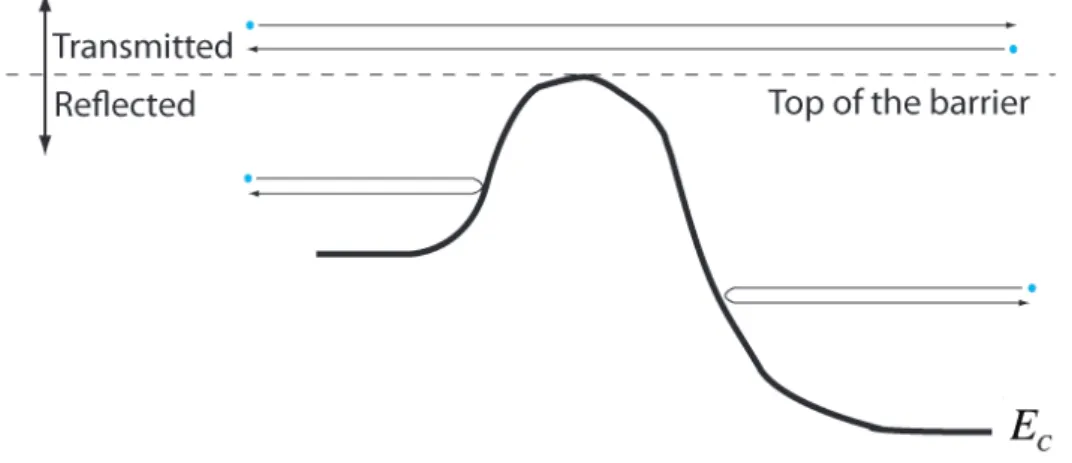
In the ballistic picture, electrons are assumed to ”ballistically” travel in the chan-nel without losing any energy or momentum. The gate however is able to modify the electrostatic potential profile in the channel by changing its bias, and electrons encountering a potential barrier higher than its energy are simply reflected back; if their energy is higher than that of the barrier, the electrons are transmitted across with total certainty. This of course is a classical treatment because we have com-pletely ignored the effect of any quantum effect such as tunneling and interferences. The ballistic picture is summarized below. It’s not hard to see the critical potential is the maximum barrier height in the channel: it’s the clear-cut point between energy
ranges for total transmission and reflection, and thus this simple semi-classical model is also known as the ”top of the barrier model”.
Fig. 2.6. Illustration of electrons injected into the channel with higher or lower energy than top of barrier.
2.5.3 Electron density in top of the barrier model
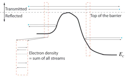
At any place in the channel, there are two types of carriers going opposite direc-tions as shown in the figure: the left going and right going ones. Each type of carrier distributes itself over a range of energies in a way described by the Fermi distribution function. If we can correctly identify the types of electrons presented, it is a simple matter of summation to determine the electron density at that point.
For illustration purpose, we will concentrate on evaluating the electron density at point A, which is a point near the source side of the channel.
From the source, left-going electrons are injected into the channel with all possible energies, and they all pass point A. Portion of them whose energy is below that of the top of the barrier is reflected back, so they pass point A as well. From the drain, right-going electrons are injected into the channel with all possible energies, but only those whose energy is higher than the top of the barrier get across and reach point A.
Fig. 2.7. Illustration of electron density evaluation at point A (red box on the left). The red box includes every possible electron ”stream”, and resulting electron density is just a simple summation of all the streams.
The electron inherits the Fermi distribution from the contact which they are injected from.
The electron density at certain energy level is defined as the product of LDOS and Fermi distribution at that energy.
n(E) =D(E)f(E) (2.45)
n(E) electron density at energy E (2.46)
D(E) local density of state at energy E (2.47)
f(E) fermi distribution of the contact injected the electron at energy E (2.48) Since we use mode space approach here, we calculate the electron density from each subband and sum all possible subbands together. In the transverse direction, we
assume everything is uniform, and electrons behave as planewaves. Let us consider the 1D electron density at point A in subband i and transverse mode j.
ni,j(A) = � ∞ 0 D1D(Ex)fs(Ex)dEx+ � Etop 0 D1D(Ex)fs(Ex)dEx + � ∞ Etop D1D(Ex)fd(Ex)dEx = � ∞ 0 1 π¯h � m∗ x 2Ex 1 1 +e(Ex+Ei+Ej−µS)/kBTdEx + � Etop 0 1 π¯h � m∗ x 2Ex 1 1 +e(Ex+Ei+Ej−µS)/kBTdEx + � ∞ Etop 1 π¯h � m∗ x 2Ex 1 1 +e(Ex+Ei+Ej−µD)/kBTdEx (2.49)
ni(A) = � ∞ 0 D1D(Ej)ni,j(A)dEj = � ∞ 0 1 π¯h � m∗ y 2Ej ni,j(A)dEj = � ∞ 0 � ∞ 0 1 π¯h � m∗ x 2Ex 1 π¯h � m∗ y 2Ej 1 1 +e(Ex+Ei+Ej−µS)/kBTdExdEj + � ∞ 0 � Etop 0 1 π¯h � m∗ x 2Ex 1 π¯h � m∗ y 2Ej 1 1 +e(Ex+Ei+Ej−µS)/kBTdExdEj + � ∞ 0 � ∞ Etop 1 π¯h � m∗ x 2Ex 1 π¯h � m∗ y 2Ej 1 1 +e(Ex+Ei+Ej−µD)/kBTdExdEj = � ∞ 0 1 π¯h � m∗ x 2Ex � m∗ y 2π 1 ¯ hF−1/2(µS−Ei−Ex)dEx + � Etop 0 1 π¯h � m∗ x 2Ex � m∗ y 2π 1 ¯ hF−1/2(µS −Ei −Ex)dEx + � ∞ Etop 1 π¯h � m∗ x 2Ex � m∗ y 2π 1 ¯ hF−1/2(µD −Ei−Ex)dEx = � m∗ xm∗y 2π¯h2 1 √ π �∞ 0 1 √ ExF−1/2(µS−Ei−Ex)dEx +√1 π �Etop 0 1 √ ExF−1/2(µS−Ei−Ex)dEx +√1 π �∞ Etop 1 √ ExF−1/2(µD −Ei−Ex)dEx (2.50)
The complete Fermi-Dirac integral of order −1/2 inside (2.50) is
F−1/2(µS−Ei−Ex) = � ∞ 0 1 √ π Ej−1/2 1 +e(Ex+Ei+Ej−µD)/kBTdEj (2.51)
In the end, we need to sum up the contributions from all subbands
n(A) = n � i=1 ni(A) = n � i=1 � m∗ xm∗y 2π¯h2 1 √ π �∞ 0 1 √ ExF−1/2(µS−Ei−Ex)dEx +√1 π �Etop 0 1 √ ExF−1/2(µS−Ei−Ex)dEx +√1 π �∞ Etop 1 √ ExF−1/2(µD −Ei −Ex)dEx (2.52)
For a point B on the right side of the top of the barrier, we can determine a similar equation using same procedure for point A.
n(B) = n � i=1 ni(B) = n � i=1 � m∗ xm∗y 2π¯h2 1 √π�0∞√1 ExF−1/2(µD −Ei−Ex)dEx +√1 π �Etop 0 1 √ ExF−1/2(µD −Ei−Ex)dEx +√1π �E∞ top 1 √ ExF−1/2(µS−Ei−Ex)dEx (2.53)
For the electron density at the top of the barrier, either formula (2.52) or (2.53) will work.
In nanoMOS, the numerical integration is carrier out by a simple composite trape-zoidal rule: � b a f(x)dx≈ b−a n � f(a) +f(b) 2 + n−1 � k=1 f � a+kb−a n �� (2.54) Infinity ∞is replaced by a large energy where the Fermi-distrubution of electrons is effectively zero. Near zero energy, due to the term √1
Ex, Ex have to be replaced by
a very small number to avoid singularity issues. The Fermi-Dirac integrals are carried out numerically [27]
2.5.4 Ballistic current
Electron density is merely a summation over all the electron streams, but when calculating current, we have to take into account their velocity (speed and direction). We will start to evaluate the current at point A as an example.
The current velocity in effective mass approximation is the derivative of electron energy spectrum at the bottom of the lowest conduction band, and it is
v = 1 ¯ h
dE
Fig. 2.8. Illustration of electron current calculation at point A (red box on the left).
v electron velocity (2.56)
For semiconductors with parabolic bands,
E = ¯h 2k2 2m∗ (2.57) Thus v = 1 ¯ h dE dk = 1 ¯ h d dk � ¯ h2k2 2m∗ � = 1 ¯ h ¯ h2k m∗ = 1 ¯ h ¯ h2 m∗ √ 2m∗E ¯ h = � 2E m∗ (2.58)
Ji,j(A) =qvni,j(A) = � ∞ 0 � 2Ex m∗ q π¯h � m∗ x 2Ex 1 1 +e(Ex+Ei+Ej−µS)/kBTdEx − � Etop 0 � 2Ex m∗ q π¯h � m∗ x 2Ex 1 1 +e(Ex+Ei+Ej−µS)/kBTdEx − � ∞ Etop � 2Ex m∗ q π¯h � m∗ x 2Ex 1 1 +e(Ex+Ei+Ej−µD)/kBTdEx = q π¯h � ∞ Etop 1 1 +e(Ex+Ei+Ej−µS)/kBTdEx − q π¯h � ∞ Etop 1 1 +e(Ex+Ei+Ej−µD)/kBTdEx (2.59)
Current density at point A in subband i is
Ji(A) = � ∞ 0 1 π¯h � m∗ y 2Ej Ji,j(A)dEj = q π¯h � ∞ 0 1 π¯h � m∗ y 2Ej �∞ Etop 1 1+e(Ex+Ei+Ej−µS)/kBT dEx −�E∞top 1 1+e(Ex+Ei+Ej−µD)/kBT dEx dEj = q π¯h2 � m∗ y 2π �∞ EtopF−1/2(µS−Ei−Ex)dEx −�E∞topF−1/2(µD −Ei−Ex)dEx (2.60)
Finally, we obtained the final current density as a summation over all possible subbands J(A) = n � i=1 Ji(A) = n � i=1 q π¯h2 � m∗ y 2π �∞ EtopF−1/2(µS−Ei−Ex)dEx −�E∞topF−1/2(µD −Ei−Ex)dEx (2.61)
This current density expression (2.61) actually holds true for all points across the channel, unlike the electron density expression which differs between the left and right