Low-Cost Signature Test of RF Blocks Based on Envelope Response
Analysis
Manuel J. Barragán, Rafaella Fiorelli, Diego Vázquez, Adoración Rueda, and José L. Huertas
Instituto de Microelectrónica de Sevilla/Centro Nacional de Microelectrónica/ Consejo Superior de Investigaciones Científicas (IMSE-CNM-CSIC)/Universidad de Sevilla
Ed. IMSE-CNM, Av. Americo Vespucio s/n, 41092 Sevilla, Spain. E-mail: [email protected]
Abstract−This paper presents a novel and low-cost methodology that can be used for testing RF blocks embedded in complex SoCs. It is based on the detection and analysis of the two-tone response envelope of the device under test (DUT). The response envelope is processed to obtain a simple digital signature sensitive to key specifications of the DUT. The analytical basis of the proposed methodology is demonstrated, and a proposal for its implementation as a built-in test core is discussed. Finally, practical simulation examples show the feasibility of the approach.
Keywords− RF test; RF BIST; Signature test
I. INTRODUCTION
Recent advances in RF CMOS technologies enable the integration of complete transceivers in a single chip, providing a significant reduction in manufacturing cost. However, there is a simultaneous increase in the cost of testing and diagnosis of these devices. Their diverse specifications and high operating frequency, as well as the large impact of process variations in current deep sub-micron technologies, make necessary extensive tests that are complex and expensive to perform. Reducing RF test complexity and cost is still an open research topic that has been addressed in a number of different approaches [1]. Recent work in this area includes defect modeling and failure diagnosis [2]-[5], alternate test [5]-[6], DfT and BIST techniques [7]-[13], etc.
In particular, BIST techniques have been identified as a solution to mitigate RF test difficulties [1]. However, an efficient BIST technique has to fulfill requirements of robustness, low area overhead, low design effort, available programming capabilities to accommodate the test program to the target measurements, and low-speed interface needs with the external ATE. Furthermore, BIST schemes (specially for complex Systems on Chip) must be based on purely-digital interpretation and take advantage of on-chip resources that admit reuse.
In this context, some recent work [14]-[15] proposes the use of an envelope detector for RF test purposes. In particular, the work in [15], recently reported by the authors, proposes an analytical and efficient method for extracting selected
functional specifications from the envelope of the response of an RF block to a two-tone test stimulus.
This work aims to extend the obtained analytical results to define a new test technique which can be used to improve the testability of RF blocks embedded in integrated transceivers, and that looks very suitable for a BIST implementation. It is based on the detection and analysis of the two-tone response envelope of an RF block by determining a digital signature which can be easily discriminated when a circuit is performing within specs. The envelope response signal is extracted using a simple envelope detector. Then, the need of RF test equipment is eliminated since the response envelope is a low frequency signal compared to the operating frequency of the tested device and it is handled by digital means. This new test procedure also reduces to a half the on-chip resources needed respect to [15].
This work is organized as follows. Section II discusses the mathematical basis of our approach from an analytical point of view. Section III defines our signature-based test procedure, together with the implementation of the signature extractor. Section IV explicits an efficient BIST implementation of the proposed test technique. After that, Section V presents some simulation examples to validate the proposal. Finally, Section VI summarizes the main contributions of the new method.
II. THEORETICAL BASIS
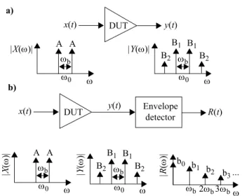
Fig.1a shows a standard two-tone test set-up that is traditionally used to characterize RF systems. In this test scheme, two high-frequency close tones are used as test stimuli and fed to the DUT. The system response is then acquired and conveniently processed to characterize the DUT. Important performance parameters such as forward gain, third-order intercept, inter-modulation products, 1dB compression point, etc, can be measured using this traditional set-up. However, the direct acquisition and processing of the test response is a challenging task, since this response is a high-frequency signal, that has to be handled by expensive RF test equipment.
Our approach, represented in Fig.1b, is in fact similar to the traditional scheme, but in this case the DUT response is driving an envelope detector. The extracted envelope has relevant information about the test response at much lower frequencies,
this information being easily extracted by simplified processing. The mathematical basis for an efficient manipulation of such an information were given in [15]. For the sake of completeness in what follows we will summarize the main steps of the procedure.
Let us consider the typical two-tone test (see Fig.1a), in which a non-linear RF device is driven by a signal x(t) composed of two equal-magnitude tones at different, but very close, frequencies, in the form,
(1) where A is the amplitude of each test tone, and ωb is the frequency difference between them. Assuming, as it is the case in most situations, a third-order non-linear model for the RF block, the response y(t) of the system can be written as,
(2) Expanding (2), and discarding the out-of-band components, the response y(t) can be expressed as [16],
(3)
In reference [15] we propose the analysis of the response envelope taking advantage of its frequency properties. Then, let R(t) be the envelope of the response signal y(t). Using the Rice formulation [17], R(t) can be derived as
(4) Signal R(t) results to be a periodic function with period
Tb=2π/ωb, and hence, can be expanded in its Fourier series as
(5) where coefficients ak=0, and b0, and bk are given, respectively,
by,
(6)
Equation (6) shows that every harmonic component of R(t) is a linear combination of the magnitudes B1 and B2, and hence, the ratio B2/B1 can be ideally derived from the frequency components of R(t). In this work, we take advantage of the spectral information contained in the response envelope to define a simple digital signature that can be used for testing purposes.
III. ENVELOPE-BASED SIGNATURE TEST The proposed test scheme requires the detection and spectral analysis of the DUT response envelope to establish a meaningful test signature. This section defines our test signatures, describes the efficient implementation of our signature extractor, and proposes a simple test methodology.
Traditional approaches for spectral analysis rely on an analog-to-digital conversion of the DUT outcome followed by the processing of the digitized signal by conventional algorithms (DFT, FFT, etc). This approach requires a full A/D converter and a complex DSP. Instead of that, since the response envelope is a low-frequency periodic function, its characterization can be made using an alternative method; in our proposal, by using a simplification of the efficient test core for periodic analog signal analysis presented by the authors in [18].
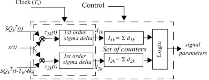
Let us review the functionality of the referenced test core, that has been depicted in Fig.2, before discussing its simplification. Let x(t) be a periodic signal of period T=2π/ω
described in terms of its Fourier series expansions in the form, (7) where x0 represents a dc level, Ak the amplitude of the k-th harmonic and ϕk its phase shift. Signal x(t) is modulated by two square waves in quadrature, SQk(t) and SQk(t-T/4k), of amplitude 1 and period T/k. The resulting signals z1k(t) and
z2k(t) are fed to two matched 1st-order Σ∆ modulators, with an oversampling ratio, N, defined as N=T/Ts (Ts is the sampling period in the Σ∆ modulators). The generated bit-streams d1k
and d2k are integrated, along an integer number M of periods of the signal under evaluation, using a set of counters to obtain two sets of digital signatures, I1k and I2k. It can be proved [18] that the digital signatures I1k and I2k are related to the signal parameters, x(t) y(t) |X(ω)| ω0 ω ωb |Y(ω)| ω0 ω ωb DUT A A B1 B2 B1 B2 x(t) y(t) |X ( ω )| ω0 ω ωb |Y(ω)| ω0 ω ωb DUT A A B1 B2 B1B2 Envelope detector R(t) |R ( ω )| ω ωb b0 b2 b1 b3 2ωb3ωb ... a) b)
Figure 1:a) Traditional two-tone test
b) Two-tone response envelope detection
x t( ) A ω0 ωb 2 ---– t cos A ω0 ωb 2 ---+ t cos + = y t( ) = α1x t( ) α+ 3x3( )t y t( ) B1 ω0 ωb 2 ---– t cos B1 ω0 ωb 2 ---+ t cos + + ≅ B2 ω0 3 ωb 2 ---– t cos B2 ω0 3 ωb 2 ---+ t cos + R t( ) 2B1 ωbt 2 ---cos 2B2 3ωbt 2 ---cos + = R t( ) b0 aksinkωbt+bkcoskωbt k
∑
>0 + = b0 4π--- B1 B2 3 ---– = bk 8π--- B1–1 ( )k+1 4k2–1 --- 3B2( )–1 k 4k2–9 ---+ = x t( ) x0 Akcos(kωt+ϕk) k∑
>0 + =(8) where magnitudes Ak are normalized to the full-scale range of the Σ∆ modulators, and phase-shifts ϕk are referenced to the rising edge of SQk(t).
This general characterization scheme can be greatly simplified by taking advantage of the two-tone response envelope properties. Equation (4) is the core of our previous method, for which the scheme in Fig.2 is valid; based on this, R(t) is expanded in a way that every harmonic component of R(t) is a linear combination of the magnitudes B1 and B2, and hence, the ratio B2/B1 can be ideally derived from the frequency components of a series expansion of R(t). However we have found that R(t) can also be expressed as,
(9) where SQ1(t) is one of the modulating square-waves
previously defined (of period 2Tb in this case). That is, the response envelope R(t) can be identified with the square-wave modulation of a low-frequency periodic signal r(t) defined as,
(10) whose two harmonic components contain, at much lower frequencies, information about the magnitudes, B1 and B2, of the spectral components of the high-frequency response y(t).
From equation (9), it is straightforward to simplify the scheme in Fig.2 to the one in Fig.3, in which only one first-order Σ∆ modulator and one digital counter are required.
The hardware requirements are roughly halved, with the corresponding savings in terms of area and power. Signature I in this simplified evaluation scheme can be directly derived as, (11) where the oversampling ratio, N, is in this case, N=2Tb/Ts, and magnitudes B1 and B2 are normalized with respect to the full-scale range of the Σ∆ modulator.
Signature I results to be a combination of the high-frequency response spectral components B1 and B2. Equation (11) allows us to compute the acceptable range of values for signature I in any given application. Then, the obtained signature can be compared with the expected ones to generate a pass/fail test decision. Functional information concerning the actual B1 and B2 values is lost, but, as an important advantage for fast production tests, the test procedure is very simple and inexpensive.
A simple test protocol for a given DUT based on the proposed concepts may be as follows:
Step 1: Definition, by DUT analysis and/or simulation, of the acceptable values of signature I according to the valid set of DUT specifications. According to (11), it is clear that signature I is sensitive to changes in gain and non-linearity specifications, so any fault affecting those characteristics may affect its value. However, it has to be taken into consideration that the sensitivity to non-linearity is usually much lower than the sensitivity to gain changes (usually B1>>B2). Hence, any device with a correct gain specification will usually lay inside the acceptance window while the effect of non-linearity over the signature is masked.
It is also important to make notice that this is only true when the two-tone test stimulus can sensitize the fault, otherwise the fault cannot be detected.
Step 2: Selection of the number of evaluation periods M. Given, as it is usual, a fixed value for the oversampling ratio in the modulator, N, then the number of evaluation periods defines the relative error in the measurement. This property can be easily derived from (11). Since the error term due to the quantization error does not scale with the number of evaluated samples, increasing M results in a lower relative error in the measurement of signature I, at the cost of longer test time.
Step 3: Extraction of the digital signature I. Finally, the extracted signature is compared to the acceptable range of values defined in step 1. A go/no-go test output signal is then generated based on this comparison.
IV. BIST IMPLEMENTATION
Although a practical implementation on silicon is beyond the goal of this paper, some general guidelines for adapting the proposed technique to a full-BIST scheme can be given. A BIST implementation is depicted in Fig.4, which only differs I1k= 2---MNπ Akcosϕk+---A33kcosϕ3k+A---55kcosϕ5k+…±2
I2k = 2---MNπ Aksinϕk+---A33ksinϕ3k+A---55ksinϕ5k+…±2
SQkT(t) SQkT(t-Tb/4k) x(t) z1k(t) z2k(t) 1st order sigma delta 1st order sigma delta d1k d2k I1k = Σ d1k I2k = Σ d2k Clock (Ts) Control
Set of counters signal
Figure 2:Test core for the characterization of periodic signals
L og ic parameters R t( ) SQ1( )t 2B1 ωbt 2 ---cos 2B2 3ωbt 2 ---cos + SQ 1( )t r t( ) = = r t( ) 2B1 ωbt 2 ---cos 2B2 3ωbt 2 ---cos + =
R(t) sigma delta1st order d I= Σ d Clock (Ts) Control
Digital counter
Figure 3:Simplified test core for the characterization of a two-tone response envelope
Logic Test
I
Result
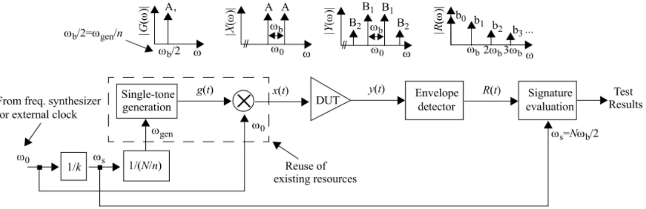
from that we proposed in [15] in the simplification of the envelope interpretation block, now substituted in Fig.4 by the signature evaluation block described in Section IV. Then, the proposed test scheme requires the generation of a two-tone RF test stimulus, the detection of the DUT response envelope, and the measurement of a digital test signature. The implementation of envelope detectors on silicon is feasible [13],[19], and the implementation of the signature extractor has already been discussed in a previous section. However, in a full-BIST implementation, signal generation has to be carefully considered together with the signature extractor, since the proposed signature definition requires a fixed, and known, oversampling ratio, N, in the Σ∆ modulator.
Usual approaches for the generation of RF test stimuli generate a low-frequency version of the desired signal and then perform an up-conversion using a mixer, which is a building block commonly available in many RF integrated systems, and hence may be adapted for its reuse during the test. In this way, the generation of a two-tone RF stimulus composed of two equal-magnitude tones at different, but very close, frequencies, such as (1), can be realized by generating a low-frequency single tone at frequency ωb/2 and mixing it with a carrier at frequency ω0, as it is depicted in Fig.4. The single-tone signal can be efficiently generated on-chip reusing existing resources in the RF system, namely an integrated DSP and a DAC, if they are available, or using simpler signal generation techniques for BIST [20]-[21] that only require a low-frequency clock to provide the desired tone. The high-frequency carrier can be provided by a frequency synthesizer (in the case this is already present in the RF system under test), or externally provided.
However, in any case, the proposed spectral analysis methodology requires the oversampling ratio N=2Tb/Ts=2ωs/ωb to be an integer number. That is, the ratio between the sampling frequency in the Σ∆ modulators forming part of the analyzer block, ωs, and the frequency of the response envelope, ωb, has to be accurately controlled. This requirement can be easily fulfilled using the clocking scheme in Fig.4. Its functionality can be described as follows. A master clock at frequency ω0 is used to clock directly the
up-conversion mixer, while a 1/k division of this master clock,
ωs, is used for the evaluation block. Given that the single-tone generator provides a signal at 1/n the frequency of its clock,
ωgen/n, then clocking the generator at a 1/(N/n) division of the evaluator clock frequency, ωgen=ωs/(N/n), achieves the desired ratio ωs=Nωb/2 by construction. In this way, choosing the values of N and n conveniently, the desired synchronization can be achieved using only simple integer divisions of a master clock.
V. APPLICATION EXAMPLE
The proposed test method has been validated by behavioral simulations in Verilog-A. The objective of these simulations is twofold: firstly, we will verify the behavior of the I-signatures predicted by (11), and after that, the I-signature discrimination capabilities will be shown.
a. Verification of the I-signature behavior
In this example, a Low Noise Amplifier (LNA) has been used as DUT. The LNA under test is driven by a two-tone at-speed stimulus, and its response envelope is extracted and processed as explained in the previous section. The goal of this test is the measurement of the I-signatures at different number of evaluation periods to verify the behavior predicted by (11).
A realistic model of the LNA has been realized according to the guidelines in [22]. Its performance figures, which are listed in Table I, correspond to typical specifications of commercial LNAs.
The envelope detector in this simulation has been modeled by a typical diode-based detector. It is important to notice that,
x(t) y(t)
DUT Envelopedetector R(t) evaluationSignature
Single-tone generation |X ( ω )| ω0 ω ωb |Y(ω )| ω0 ω ωb A A B1 B2 B1B2 |R(ω )| ω ωb b0 b 2 b1 b 3 2ωb3ωb ... Test g(t) |G ( ω )| ω ωb/2 A‚ Results 1/k 1/(N/n) ωgen ω s=Nωb/2 ω0 ω0 ωs ωb/2=ωgen/n
Figure 4:Proposal for a full-BIST implementation From freq. synthesizer
or external clock
Reuse of existing resources
TABLE I:Simulation parameters LNA
specifications GainIIP3 16dBm16dB
NF 1dB Σ∆ modulators fs/fb 96 FS 500mV Test stimulus A 15mV f0 1GHz fb 1MHz
although an actual implementation can vary from a diode-based one, in any case there is no need of an accurate envelope detector, since accuracy is much more dependent of parameters M and N. The ripple voltage introduces high frequency components that will be attenuated by the proposed spectral analysis method. The simulation parameters used for the LNA and the Σ∆ modulator are listed in Table I.
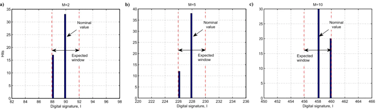
A set of Monte Carlo simulations was performed in order to validate the use of the proposed digital signature. Since this verification is aimed to test the signature definition itself and not the LNA, the LNA specifications were kept constant in these simulations. The experiment was repeated for three different number of evaluation periods M. Fig.5 shows histograms of the obtained I-signatures, together with the nominal I value obtained by simulation in the typical case. As expected, the obtained signatures agree with the analytically predicted -window defined by equation (11) in all cases.
b. Faulty behavior detection capability
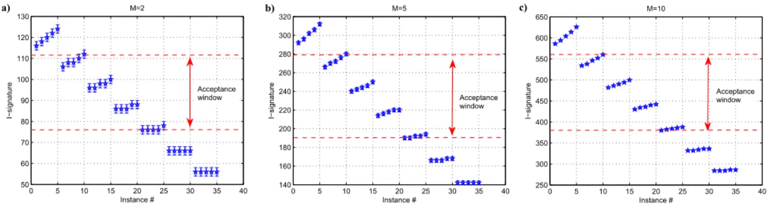
In this example, a set of different instances of the previous LNA was generated varying its gain and linearity specifications from the nominal ones in Table I. The generated instances and their specifications are listed in Table II.
Signature I was extracted for each instance and represented in Fig.6, for three different number of evaluation periods M. The acceptance windows in these examples have been defined according to a usual variation in the LNA specs for a typical nanometric CMOS process. In this case, a gain variation and an IIP3 above 15dBm were defined as acceptable.
As it is shown in Fig.6, all the instances with a correct gain specification lay inside the acceptance window for the three M cases considered, while the ones with an incorrect gain lay outside. It is also clear that the relative error in the signature decreases when M increases, as predicted by (11). As it was also expected, the effect of IIP3 variation above the accepted values, although it modifies the value of the signature, it is not enough to move the signature out of the acceptance window. This test method is then very suitable for quickly discarding
devices with a faulty gain, but detecting non-linearity variations demands a different approach.
VI. CONCLUSIONS
A novel methodology for testing embedded RF blocks has been presented. It is based on the analysis of the envelope of the system response to a two-tone at-speed stimulus. This methodology is an efficient modification of a previous one already published by the authors, but differs in an important simplification of the test interpretation, which is now based on a digital signature.
From a hardware point of view, the proposed test core is reduced to a simple low-performance envelope detector, together with a first-order Σ∆ modulator and a digital counter, while the generation of the test stimulus can be easily performed reusing on-chip resources.
2 ± 3σ ± 1.5dB ±
TABLE II:LNA instances
Instance # Gain
(dB) (dBm)IIP3 Instance # Gain (dB) (dBm)IIP3
1 18 20.3 19 15.6 16.6 2 18 19.3 20 15.6 16 3 18 18.5 21 14.5 18.5 4 18 17.8 22 14.5 17.5 5 18 17.3 23 14.5 16.7 6 17.3 20 24 14.5 16 7 17.3 19 25 14.5 15.5 8 17.3 18 26 13.4 18 9 17.3 17.5 27 13.4 17 10 17.3 17 28 13.4 16 11 16.5 19.5 29 13.4 15.5 12 16.5 18.5 30 13.4 15 13 16.5 17.7 31 12 17.3 14 16.5 17 32 12 16.3 15 16.5 16.5 33 12 15.5 16 15.6 19 34 12 14.8 17 15.6 18 35 12 14.3 18 15.6 17.3 450 452 454 456 458 460 462 464 466 0 5 10 15 20 25 30 M=10 Digital signature, I Hits Nominal value Expected window 220 222 224 226 228 230 232 234 236 0 5 10 15 20 25 30 35 40 M=5 Digital signature, I Hits Expected window Nominal value 82 84 86 88 90 92 94 96 98 0 5 10 15 20 25 30 35 Digital signature, I Hits M=2 Expected window Nominal value a) b) c)
Future work in this line includes the development of an integrated demonstrator comprising a LNA, the envelope detector, and the proposed signature extractor in a 90nm CMOS technology.
Advantages of the presented approach are that there is no need of high-frequency signal processing nor of a full A/D converter, reducing the test interpretation to a 1st-order modulator and a purely digital circuit. This makes the proposed test core simple to implement and very suitable for its inclusion in an on-chip BIST scheme.
ACKNOWLEDGEMENTS
This work has been funded in part by the Spanish Government through a JAE-DOC contract, and projects TEST (TEC2007-68072/MIC), SR2 (TSI-020400-2008-71/MEDEA+ 2A105), TOETS (CATRENE/MEDEA+2 CT302) and by the Junta de Andalucia through project ACATEX (P09-TIC-5386).
REFERENCES
[1] M. J. Barragan, G. Huertas, A. Rueda, J. L. Huertas, “(Some) Open Problems to Incorporate BIST in Complex Heterogeneous Integrated Systems”, Proc. of the 5th IEEE International Symposium on Electronic Design, Test, and Applications (DELTA 2010), pp. 8-13.
[2] E. Acar, S. Ozev, “Defect-based RF testing using a new catastrophic fault model”, IEEE International Test Conference, Nov. 2005.
[3] E. Acar, S. Ozev, “Diagnosis of the failing components in RF receivers through adaptative full-path measurements”, Proc. VLSI Test Symposium, May 2005, pp. 374-379.
[4] M. S. Heutmaker, D. K. Le, “An architecture for self-test of a wireless communication system using sampled IQ modulation and boundary scan”, IEEE Communication Magazine, 1999, vol 37, no 6, pp. 98-102. [5] A. Halder, S. Bhattacharya, G. Srinivasan, A. Chatterjee, “A system level
alternate test approach for specification test of RF transceivers in loopback mode”, Proc. VLSI design, 2005.
[6] R. Voorakaranam, S. Cherubal, A. Chatterjee, “A signature test framework for rapid production testing of RF circuits” Proc. DATE 2002, pp. 186-191.
[7] A. Yin, W. R. Eisenstadt, R. M. Fox, T. Zhang, “A Translinear RMS detector for embedded test of RF ICs”, IEEE Transaction on Instrumentation and Measurement, 2005, vol. 54, no. 5, pp. 1708-1714. [8] J. Ryu, B. C. Kim, I. Sylla, “A new low-cost RF built-in self-test
measurement for system-on-chip transceivers” IEEE Trans. Instrumentation and Measurement, 2006, vol 55, no. 2, pp. 381-388. [9] A. Gopalan, T. Das, C. Washburn, P. R. Mukund, “An ultra-fast on-chip
BIST for RF low noise amplifiers” Proc. VLSI design, 2005, pp. 485-490. [10] A. Valdes Garcia, J. Silva Martinez, E. Sanchez Sinencio, “On-chip testing techniques for RF wireless transceivers”, Design and Test of Computers, July-August 2006, pp. 268-277.
[11] A. Valdes Garcia, W. Khalil, B. Bakkaloglu, J. Silva Martinez, E. Sanchez Sinencio, “Built-in Self Test of RF Transceiver SoCs: from Signal Chain to RF Synthesizers”, Proc. of the IEEE Radio Frequency Integrated Circuits Symposium, 2007.
[12] S. S. Akbay, A. Chatterjee, “Built-in Test of RF components using mapped feature extraction sensors” Proc. VLSI Test Symposium, 2005, pp. 243-248.
[13] S. Khulalli, S. Seth, S. Fu, “An integrated linear RF power detector”, Proc ISCAS 2004.
[14] D. Han, S. Bhattacharya, A. Chatterjee, “Low-cost parametric test and diagnosis of RF systems using multi-tone response envelope detection”, IET Comput. Digit. Tech., vol 1, no 3, 2007, pp.170-179.
[15] M. J. Barragan, R. Fiorelli, D. Vázquez, A. Rueda, J. L. Huertas, “On-chip characterisation of RF systems based on envelope response analysis”, IET Electronics Letters, vol. 46, no.1, 7th January 2010.
[16] B. Razavi, “RF Microelectronics”, Prentice Hall PTR, Upper Saddle River, NJ, USA, 1998.
[17] J. Dugundji, “Envelope and pre-envelopes of real waveforms”. IEEE Trans. Inform. Theory, vol 4, no 1, pp. 53-57, 1958.
[18] D. Vázquez, G.. Huertas, A. Luque, M. J. Barragán, G. Leger, A. Rueda, J. L. Huertas, “Sine-Wave Signal Characterization Using Square-Wave and SD-Modulation: Application to Mixed-Signal BIST”, Journal of Electronic. Testing: Theory and Applications, vol 21, pp 221-232, 2005. [19] Y. Zhou, G. Huang, S. Nam, B. Kim, “A Novel Wide-Band Envelope
Detector”, Proc. of the IEEE Radio Frequency Integrated Circuits Symposium, 2008, pp. 219-222.
[20] M. J. Barragan, D. Vazquez, A. Rueda, J. L. Huertas, “On-chip analog sinewave generator with reduced circuitry resources”, Proc. of the 49th IEEE International Midwest Symposium on Circuits and Systems (MWSCAS’06), August 2006.
[21] B. Dufort, and G. W. Roberts, “On-chip analog signal generation for mixed-signal Built-in Self-Test”, IEEE Journal of Solid-State Circuits, 1999, vol. 33, n. 3, pp. 318-330.
[22] Jinsong Zhao, “Behavioral modeling of RF circuits in Spectre”, Cadence White Paper, available on-line: http://www.cadence.com/datasheets/dat_pdf/rf_behavioral.pdf. 0 5 10 15 20 25 30 35 40 50 60 70 80 90 100 110 120 130 M=2 Instance # I−signature Acceptance window 0 5 10 15 20 25 30 35 40 140 160 180 200 220 240 260 280 300 320 M=5 Instance # I−signature Acceptance window 0 5 10 15 20 25 30 35 40 250 300 350 400 450 500 550 600 650 Instance # I−signature M=10 Acceptance window
Figure 6:Signature test results: a)M=2, b)M=5, c)M=10