Architecting Memory Systems for Emerging Technologies
byByoungchan Oh
A dissertation submitted in partial fulfillment of the requirements for the degree of
Doctor of Philosophy (Electrical Engineering) in the University of Michigan
2018
Doctoral Committee:
Professor Trevor N. Mudge, Co-Chair
Assistant Professor Ronald G. Dreslinski Jr., Co-Chair Professor David Blaauw
Byoungchan Oh [email protected]
ORCID iD: 0000-0001-9612-2501
© Byoungchan Oh 2018 All Rights Reserved
ACKNOWLEDGMENTS
I would like to thank my primary advisor, Professor Trevor Mudge, for his invaluable sup-port and guidance. I appreciate everything he has done for me. No words can express my gratitude to him. Professor Ronald Dreslinski, my co-advisor, has perfectly comple-mented Trev. I also would like to thank my dissertation committee members, Professor David Blaauw and William Martin, for their wisdom and guidance in the final steps of my studies.
I am pleased to have met lifelong friends in TRON lab: Antony Gutierrez, Qi Zheng, Nilmini Aberaytne, Yajing Chen, Cao Gao, Jonathan Beaumont, Dong-Hyeon Park, Yiping Kang, and Johann Hauswald. I shall never forget the countless hours and moments together. I especially appreciate the kindness, consideration, and help of Nilmini during whole my Ph.D. study and life. I would like to thank all those who directly and indirectly have helped my studies: Doowon Lee, Yongkee Kwon, Jihyae Bae, Dong-Keun Kim, Professor Jeongseob Ahn, and Professor Nam Sung Kim.
Lastly and most importantly, I would like to thank my parents and brother. I am forever grateful for their unwavering faith and support. To my loves, Blue, Berry and Mijung, I could finish my studies thanks to you. I owe much of my successes to my wife and her devotion to my family.
TABLE OF CONTENTS
Dedication . . . ii
Acknowledgments . . . iii
List of Figures . . . vi
List of Tables . . . viii
Abstract. . . ix
Chapter 1 Introduction . . . 1
1.1 Memory System . . . 1
1.2 Memory Technology . . . 2
1.3 Emerging Memory Technology . . . 6
1.4 Dissertation Organization . . . 8
2 STT-MRAM Architecture for Smart Activation and Sensing . . . 9
2.1 Introduction . . . 10
2.2 Challenges in Architecting STT-MRAM . . . 13
2.2.1 Large Sense Amps with High Power Consumption . . . 13
2.2.2 Limitations with Shared Sense Amps . . . 14
2.3 SMART Architecture . . . 17 2.3.1 Re-architecting STT-MRAM . . . 18 2.3.2 Benefits . . . 20 2.3.3 Discussion . . . 26 2.4 Device Modeling . . . 28 2.4.1 Area Model . . . 29 2.4.2 Timing Model . . . 30 2.4.3 Energy Model . . . 30 2.5 Evaluation . . . 32 2.5.1 Evaluation Methodology . . . 32 2.5.2 Performance . . . 33 2.5.3 Energy . . . 35 2.5.4 Sensitivity Analysis . . . 38 2.6 Related Work . . . 39
2.7 Summary . . . 40
3 Improving Load Balancing for Memory Channels . . . 41
3.1 Introduction . . . 42
3.2 Background . . . 44
3.2.1 Increasing Demand of Memory Capacity and Bandwidth . . . 44
3.2.2 High Bandwidth Memory . . . 44
3.3 Challenges in Many Channel Memory Systems . . . 48
3.3.1 Imbalanced Channel Utilization . . . 48
3.3.2 Implementation Challenges of Memory Controllers . . . 50
3.4 Overview of the Proposed Design . . . 52
3.4.1 Re-architecting Memory Controllers . . . 53
3.4.2 Re-architecting HBM . . . 58 3.4.3 Overhead . . . 59 3.5 Evaluation . . . 61 3.5.1 Methodology . . . 61 3.5.2 Performance Analysis . . . 62 3.5.3 Area Overhead . . . 65 3.6 Related Work . . . 66 3.7 Summary . . . 67 4 Conclusion . . . 69 Bibliography . . . 71
LIST OF FIGURES
1.1 Von Neumann architecture. . . 1
1.2 Memory hierarchy. . . 2
1.3 DRAM scaling trend [1]. . . 3
1.4 Increasing throughput loss and power consumption by refresh [2]. . . 3
1.5 Impacts of the DRAM page size in STREAM benchmark [3]. . . 4
1.6 Increasing data rate from SDR to DDR4. . . 5
1.7 STT-MRAM cell structure and MTJ. . . 6
1.8 2.5D integration between HBM and GPU through a interposer. . . 7
2.1 Bank architecture and operation of DRAM (left) and conventional STT-MRAM (right). . . 15
2.2 SMART bank architecture and data/control flow. . . 18
2.3 Change of read and write accesses after making sensing operation triggered by aRDcommand. . . 19
2.4 SMART page mode and enhanced bank architecture. . . 20
2.5 Relation between page size andACTenergy. . . 21
2.6 Impact oftRRDon bank-level parallelism. . . 22
2.7 tRRD and tFAW for various page sizes. tRRD and tFAW for DRAM are obtained from a DDR3 datasheet [4]. . . 23
2.8 Comparison of the three repair schemes. . . 24
2.9 Change of row access cycle on row misses. . . 25
2.10 Row hit rate in various workloads. . . 34
2.11 Read latency profile of mix6 workload. . . 35
2.12 Performance improvement compared to DRAM. . . 36
2.13 Energy savings over DRAM. . . 36
2.14 Breakdown of average memory power. . . 37
2.15 Normalized performance improvement and energy saving of the conventional STT-MRAM (Conv-Delay) to the baseline DRAM with various page size. . . . 38
2.16 Normalized IPC and energy to DRAM with various configurations (average of all mix workloads). . . 39
3.1 GPU systems with GDDR5 and HBM. . . 45
3.2 3D structure of HBM and a simple example of TSV connection to DRAM dies. 46 3.3 Comparison between two memory organizations [5]. . . 47
3.5 Simple diagram for work stealing. . . 49
3.6 Performance according to queue depth. . . 50
3.7 Schedulers of the memory controller in many channel memory systems [6]. . . 51
3.8 Hierarchical queue structure. . . 53
3.9 Limited scheduling. . . 55
3.10 Avoiding timing constraint. . . 56
3.11 HBM with crossbars. . . 60
3.12 Performance improvement after the migration. . . 63
3.13 Change of imbalanced memory service time. . . 63
3.14 MPKI and locality. . . 64
LIST OF TABLES
2.1 Comparison with previous studies . . . 27
2.2 Area comparison . . . 29
2.3 Timing and latency comparison . . . 30
2.4 Energy and current comparison . . . 31
2.5 Default system configuration . . . 33
2.6 Workloads for multi-core simulations . . . 33
3.1 Configured System . . . 61
3.2 Workload list . . . 62
ABSTRACT
The advance of traditional dynamic random access memory (DRAM) technology has slowed down, while the capacity and performance needs of memory system have continued to in-crease. This is a result of increasing data volume from emerging applications, such as machine learning and big data analytics. In addition to such demands, increasing energy consumption is becoming a major constraint on the capabilities of computer systems. As a result, emerging non-volatile memories, for example, Spin Torque Transfer Magnetic RAM (STT-MRAM), and new memory interfaces, for example, High Bandwidth Mem-ory (HBM), have been developed as an alternative. Thus far, most previous studies have retained a DRAM-like memory architecture and management policy. This preserves com-patibility but hides the true benefits of those new memory technologies.
In this research, we proposed the co-design of memory architectures and their manage-ment policies for emerging technologies. First, we introduced a new memory architecture for an STT-MRAM main memory. In particular, we defined a new page mode operation for efficient activation and sensing. By fully exploiting the non-destructive nature of STT-MRAM, our design achieved higher performance, lower energy consumption, and a smaller area than the traditional designs. Second, we developed a cost-effective technique to im-prove load balancing for HBM memory channels. We showed that the proposed technique was capable of efficiently redistributing memory requests across multiple memory channels to improve the channel utilization, resulting in improved performance.
CHAPTER 1
Introduction
1.1
Memory System
A memory system is one of the core sub-systems in modern computer architectures. Mod-ern computer architectures are based on Von Neumann architecture which mainly con-sists of memory, input/output, the arithmetic/logic unit, and the control unit as shown in Fig.1.1[7,8]. The memory in Von Neumann architecture stores program data and instruc-tion data. Thus, this architecture is sometimes called to a stored-program computer [9]. Because storing data to memory and loading data from memory are essential operations in this architecture, performance and energy consumption of the memory system signifi-cantly affect overall system performance and energy consumption [10–12]. Moreover, the importance of a memory system continuously is increasing with emerging applications and services which need more memory capacity and bandwidth [13–15] .
MEMORY
CPU
CONTROL
UNIT
ARITHMETIC
LOGIC UNIT
INPUT
OUTPUT
CODE
DATA
REGISTER
CACHE
Main Memory
STORAGE
CPU
FA
ST
ER
LA
RG
ER
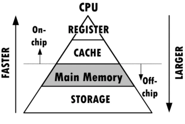
On-chip Off-chipFigure 1.2: Memory hierarchy.
Memory systems have evolved with a hierarchical structure as shown in Fig.1.2 [16]. This structure can take both advantages of short access time offered from small memories (e.g, register files and caches) and area efficiency provided from large memories (e.g, main memory and storage). A main memory is not too fast, but not too small. Because the different process technology from that of CPU is used for main memories, they are typically off-chip devices. Generally, the main memory holds whole program code and data whereas caches temporally hold partial code and data1. Thus, there are frequent accesses to the main
memory in irregular applications, where cached data are not reused well. Besides, recent in-memory database techniques increase use of the main memory [14,17].
1.2
Memory Technology
Memory Cell. Dynamic Random Access Memory (DRAM) is a type of random access semiconductor memory that stores each bit of data in a separate tiny capacitor. It is used as the main memory in most computing systems. As the de facto standard in the past several decades, DRAM has been continuously increased in capacity as shown in Fig.1.3. However, after increasing for decades, the capacity of DRAM nowadays has now stopped at 8 Gb. The root cause resulting in this trend is DRAM’s refresh operation. Because the cell capacitor is leaky, DRAM cells must be periodically refreshed to prevent data loss
1985 1990 1995 2000 2005 2010 2015 2020 1Mb 4Mb 16Mb 64Mb Year D en si ty 128Mb256Mb 512Mb 1Gb2Gb 4Gb 8Gb ? ? ?
Figure 1.3: DRAM scaling trend [1].
20 20 60 80 0 100 2Gb 4Gb 8Gb 16Gb 32Gb 64Gb Th ro ug hp ut L os s [% ] Density
(a) Throughput loss by refresh
0 350 2Gb 4Gb 8Gb 16Gb 32Gb 64Gb Po w er C on su m pt io n [m W ] Density 300 250 200 150 100 50 Refresh Power Non-refresh Power
(b) Relative power consumption of refresh
Figure 1.4: Increasing throughput loss and power consumption by refresh [2].
within their retention time (typically 64 ms). Unfortunately, this retention time has not improved.2 If DRAM capacity is increased without improvement of retention time, more DRAM cells must be refreshed within the same period. Thus, the relative time spent for refresh is increased according to the capacity. This increased refresh time can be converted to throughput loss as shown in Fig.1.4a. Furthermore, the power consumption for refresh is also increased in proportion to capacity. The refresh power consumption, which does not contribute to computation, will become comparable with the dynamic power consumption, which is directly involved with the computation as shown in Fig.1.4b.
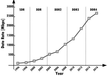
Memory Interface. Double Date Rate (DDR), which is successors to Single Data Rate 2In fact, the retention time is becoming worse and thus some recent DRAM devices have shorter retention time (32ms) than the normal 64ms[18].
0.5 0.6 0.7 0.8 0.9 1.0 IP C [ N o rm .]
Page Size [Byte]
(a) Performance 0.5 0.6 0.7 0.8 0.9 1.0 M e mo ry P o w e r [N o rm. ]
Page Size [Byte]
(b) Memory power
Figure 1.5: Impacts of the DRAM page size in STREAM benchmark [3].
(SDR), is the most widely used interface standard for a main memory. In DDR memories, a memory access is divided into two types of accesses, row access and column access. A row access command activates or deactivates a row in a memory array. When a row is activated, all cells connected to that row are sensed by sense amps and the sensed data are stored in row buffers. Because data are already stored in the row buffer, a following column access command can be served from the row buffer without additional array access.3 Also,
a following column access going to the same row can be served without additional row access, because all data for the row are already stored in the row buffer. This operation is calledpage modeoperation and still remains unchanged in modern DDR devices. The size of data sensed by a row activation command is defined as page size. In general, page mode increases performance by avoiding repeated activation of the same row to access different columns. Thus, the large page size is good for performance especially when data locality is high. However, the wasted energy is increased in large pages because all data in a page (i.e, the row buffer) are not used always. As shown in Fig. 1.5, it is hard to capture both high performance offered by large pages and low power consumption offered by small pages at the same time [19–22].
3A read command can immediately read out data stored in the row buffer, but a write command needs to access the array after updating data in the row buffer. However, after updating the row buffer but before finishing array access, another column access is allowed.
500 1000 1500 2000 2500 3000 Year D at e Ra te [M bp s] SDR DDR DDR2 DDR3 DDR4 1998 2000 2002 2004 2006 2008 2010 2012 2014 2016 1996
Figure 1.6: Increasing data rate from SDR to DDR4.
Total peak memory bandwidth is defined as,
M emory Bandwidth=Data Rate×Bus W idth×N umber of Channels (1.1) where data rate is equal to memory bus clock speed in SDR and double of the clock speed in DDR, bus width is traditionally is 64 bits, and the number of channels is typically 1∼6 for main memory systems. As shown in Fig. 1.6, data rate from SDR to DDR4 has been continuously increased. That is, traditionally memory bandwidth has been increased by increasing data rate (i.e, clock speed). However, increasing the clock speed has several challenges. First, the clock speed in latest DDR generation is already 1.2 GHz and it is fast enough. There will be some degree of increase in the clock speed, but that would not be an order of magnitude increase. That is, it is hard to achieve an order of magnitude higher memory bandwidth by increasing the clock speed. Second, generally faster clock requires higher supply voltage. Although technology improvements such as low voltage swing termination logic (LVSTL) suppress the increase of the supply voltage, increasing clock speed cannot save power consumption.
Bitline (BL) Source line (SL) Wordline (WL)
MTJ
(a) Bit-cell structure of STT-MRAM
MTJ Storage layer
Tunneling barrier Reference layer
Parallel state (P)
Anti-Parallel state (AP)
Low resistance (RP)
High resistance (RAP)
(b) Magnetic Tunneling Junction
Figure 1.7: STT-MRAM cell structure and MTJ.
1.3
Emerging Memory Technology
Memory Cells Technology. Because of DRAM’s refresh and the limitations caused by it, emerging non-volatile memories such as Resistive RAM (ReRAM), Phase Change Memory (PCM) and Spin Transfer Torque Magnetic RAM (STT-MRAM) have been receiving more attention. However, unlike other emerging non-volatile memories, STT-MRAM is consid-ered to be a replacement candidate for a main memory because of its fast access speed and high endurance [23–29]. An STT-MRAM cell consists of an access transistor and a Mag-netic Tunneling Junction (MTJ) to store data as shown in Fig.1.7a. There are three layers in an MTJ: two magnetic layers and one tunneling barrier between them as shown in Fig.1.7b. The “reference” magnetic layer has a fixed magnetization and the “free/storage” layer has a variable magnetization. When their magnetization directions are the same (parallel state, P), an MTJ shows low electrical resistance (RP). When their magnetization directions are
different (anti-parallel state, AP), they show high resistance (RAP). This change in the
re-sistance is called the tunneling magnetorere-sistance effect. The spin transfer torque (STT) force is exerted by injecting a spin-polarized current to change the magnetization direction of the free/storage layer. In order to enable bi-directional change, a bi-directional current should flow through an STT-MRAM cell. Therefore, one terminal of an MTJ is connected to a bit-line (BL) through a selection transistor and the other terminal is connected to a
Logic Die DRAM Die DRAM Die DRAM Die DRAM Die DRAM Die DRAM Die DRAM Die DRAM Die GPU Interposer
Figure 1.8: 2.5D integration between HBM and GPU through a interposer.
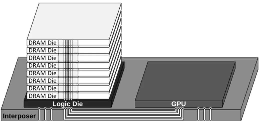
source-line (SL) for the write operation as shown in Fig.1.7a [30,31]. Although this cell structure is similar to a DRAM cell structure, the STT-MRAM cell is larger due to the larger access transistor. The larger access transistor is required to drive enough current to switch the magnetization direction. Alternatively, increasing the write time (pulse width) can reduce the amount of current required and thus the cell size can be smaller [32,33]. Memory Interface Technology.There are variants of DDR standard for specialized appli-cations: Low Power DDR (LPDDR) optimized for power consumption and Graphic DDR (GDDR) optimized for performance. Although several unique features exist in LPDDR or GDDR such as Partial Array Self Refresh (PASR) in LPDDR and separate higher speed Write Clock (WCK) in GDDR, their basic operations are almost same as normal DRAM [5, 18,34]. Besides, they all use narrow (32∼64 bits per channel) and fast (up to 7Gbps per pin) memory channels. Because of this narrow and fast channel, increasing memory capacity and bandwidth is limited by the power budget. Moreover, accommodating more memory chips to achieve higher the capacity and bandwidth can limit the form factor. In order to overcome this issues, 3D stacked DRAM memories, such as High Bandwidth Memory (HBM) and Wide I/O (WIO), have been developed [35,36]. In Fig.1.8, an example of 2.5D integration between a processor (GPU) and a stacked DRAM (HBM) through a silicon in-terposer is described. Because the interconnections through the inin-terposer are much shorter
than the interconnections between off chips on PCB, the data transfer energy is lower on the interposer. In addition, a stack of DRAM dies in HBM provides multiple channels (up to 8) within a small space and the interposer can accommodate all I/Os for the channels. Because the bandwidth is linearly proportional to the data rate and total number of I/Os for all channels, HBM’s large number of I/Os (1024 vs. 32 for GDDR5) allows to lower the data rate (2Gbps vs. 7Gbps for GDDR5) while increasing the bandwidth (256GB/s vs. 28GB/s for GDDR5).
1.4
Dissertation Organization
The research work is organized as follows. Chapter2presents a co-design of memory ar-chitecture and its management policy for an STT-MRAM main memory. Chapter3presents a cost-effective technique to improve load balancing for HBM channels. Finally, Chapter.4
CHAPTER 2
STT-MRAM Architecture for Smart Activation
and Sensing
STT-MRAM is a promising memory technology as a drop-in replacement of DRAM for main memory, because it can offer higher energy efficiency than DRAM with latency com-parable to DRAM. However, STT-MRAM needs to employ current sense amps which con-sume an order of magnitude larger space and power than voltage sense amps adopted by DRAM. Consequently, to manage the high cost of sense amps, STT-MRAM decouples bit-lines from sense amps and shares one sense amp with 16∼128× bit-lines, exploiting the non-destructive nature of its read operation. However, such STT-MRAM reduces the size of row buffers and incurs more row-buffer misses (i.e, higher activation energy and lower performance) than DRAM along with other issues, especially when it follows interfaces and policies designed for DRAM.
To cost-effectively address these issues, we propose SMART, co-designing STT-MRAM architecture and its management policy in this study. Specifically, unlike DRAM and con-ventional STT-MRAM, SMART proposes to sense bit-lines after receiving a column access command instead of a row activation command. This can provide several benefits including larger pages, fewer sense amps, lower activation/sensing power, shorter latency, fewer ad-dress pins and more efficient repairs of defective columns than conventional STT-MRAM. Our evaluation shows that SMART consumes 11% (39%) lower energy while providing 9% (5%) higher performance than conventional STT-MRAM (DRAM) on average. In addition
to these benefits, SMART is 6% smaller than conventional STT-MRAM.
2.1
Introduction
STT-MRAM is one of the promising emerging non-volatile memory (NVM) technologies as a drop-in replacement of DRAM for main memory because of its faster speed and higher endurance than other NVM technologies [23–29]. However, STT-MRAM has some dis-advantages over DRAM. One of such disdis-advantages is a need to use large and high-power sense amps in STT-MRAM. Specifically, STT-MRAM needs current sense amps consum-ing an order of magnitude larger space and higher power than voltage sense amps adopted by DRAM. To manage the cost of implementing such sense amps, STT-MRAM leverages the non-destructive nature of its read operation and shares one sense amp with 16∼128 bit-lines in each bank [37–42]. Such STT-MRAM architectures, nonetheless, suffer from two limitations.
First, STT-MRAM with fewer sense amps provides smaller row buffers and thus pages than DRAM, as the number of sense amps determines the size of row buffers [16]. Larger pages provide higher performance with more row-buffer hits when data locality is high, but they consume more energy when data locality is poor, which is also known as the overfetching problem. In contrast, smaller pages consume less energy when data locality is poor, but they give lower performance with more row-buffer misses when data locality is good. The size of STT-MRAM row buffers is far smaller than that of DRAM row buffers but much larger than that of a column access. Therefore, STT-MRAM suffers from more row-buffer misses than DRAM without completely eliminating the overfetching problem.
Second, when such STT-MRAM uses interfaces and policies designed for DRAM, it suffers from a column address fragmentation problem [27,42]. Specifically, DRAM re-quires sense amps to sense all 16,384 bit-lines in a sub-array and latch the data until
open-ing another row due to the destructive nature of its read operation. Therefore, for a given row address, DRAM performs both activation and sensing at the same time with a single row activation (ACT) command. However, it becomes problematic to directly apply such an activation/sensing approach to STT-MRAM with fewer sense amps than the number of bit-lines (i.e, size of a row), because STT-MRAM must receive both a row address and some of a column address at the same time to connect a sub-set of chosen bit-lines to the sense amps through multiplexers when activating a row. That is, STT-MRAM with the same capacity as DRAM requires more address pins to send not only a row address but also some of a column address together with a row command1. Besides, such a fragmentation of a column address between row and column commands considerably worsens efficiency and flexibility of column repair mechanisms as a row or column command has only partial column address information [43,44].
To cost-effectively address these issues, we propose SMART,STT-MRAMARchiTecture supporting smart activation/sensing. Specifically, exploiting one of the advantages of STT-MRAM, non-destructive nature of its read operation, we propose to provide only 64 sense amps2for each bank and make a column access command instead of a row activation com-mand sense bit-lines. This deceptively simple change, which is not possible for DRAM with the destructive nature of its read operation, can offer the following advantages over conventional STT-MRAM.
(1) SMART offers the illusion of providing 16× larger row buffers with 16× fewer sense amps than conventional STT-MRAM. That is, SMART provides 2KB pages with only 64 sense amps per bank, whereas conventional STT-MRAM gives 128B pages with 1,024 sense amps per bank. Furthermore, conventional STT-MRAM repeatedly consumes long time (tRC = 27.5ns) and high power to access the same row but columns which 1DRAM uses the same set of address pins to receive both row and columns addresses in a time multiplexed manner. Since a row address typically needs more bits than a column address, the number of row address bits determines the number of address pins in DRAM.
2In this study, we assume DRAM and STT-MRAM modules, each consisting of eight×8 devices for 64-bit I/O. Therefore, each device must sense 64 64-bits to support the burst length of 8 for a single column access command.
were not selected and sensed by the previous row command. This is because conventional STT-MRAM needs to recognize such memory accesses as row-buffer misses to select and sense different bit-lines. In contrast, SMART can recognize such memory accesses as row-buffer hits and it only needs another column access command because it selects and senses different bit-lines which were already connected to the necessary cells by the previous row activation command.
(2) SMART consumes∼88% lower activation power than conventional STT-MRAM. Specifically, conventional STT-MRAM senses 1,024 bit-lines as part of a row activation, and sensing power dominates the activation power. In contrast, SMART consumes 16×
less sensing power than conventional STT-MRAM because it senses only 64 bit-lines (i.e, granularity of a column access) as part of a column access. Hence, SMART practically eliminates the overfetching problem. Furthermore, whenever a memory write access de-mands an activation of another row, conventional STT-MRAM unnecessarily consumes sensing power because sensing is part of the row activation. However, SMART does not consume any sensing power for such a memory write access, because sensing is not part of a row activation but part of a column read access.
(3) SMART offers shorter latency for memory accesses. Specifically, high sensing power imposes tRRD and tFAW constraints in DRAM and STT-MRAM and limits the number of row activation commands in a certain time period. As SMART significantly reduces sensing power, it can eliminates these two constraints and handle more row acti-vation commands in a shorter time period than conventional STT-MRAM. As previously mentioned, conventional STT-MRAM performs sensing as part of row activation while sensing is unnecessary for memory write accesses. Moreover, sensing constitutes a notable fraction of activation time. Therefore, SMART can also reduce latency of memory write accesses especially to different rows compared with conventional STT-MRAM.
(4) SMART needs fewer pins and offer 10.7×more efficient repairs of defective columns than conventional STT-MRAM. Particularly, SMART does not sense bit-lines as part of
row activation. Therefore, it does not need to select and connect specific bit-lines to sense amps as part of row activation. That is, it only needs to receive a row address for activation like DRAM. Besides, SMART receives the full column address with a column command, it can use the same efficient mechanism as DRAM for repairing defective bit-lines.
(5) SMART eliminates the need for sending separate pre-charge commandssince a col-umn command can comprise the function of a pre-charge command. As a result, SMART not only offers 11% shorter latency for memory accesses which are directed to the same bank but incur row-buffer misses, but also consumes less command bus bandwidth than conventional STT-MRAM.
In summary, (1)–(5) not only reduce energy but also improve performance. Our eval-uation shows that SMART consumes 11% (39%) lower energy while providing 9% (5%) higher performance than conventional STT-MRAM (DRAM) on average. In addition to these benefits, SMART is 6% smaller than conventional STT-MRAM.
2.2
Challenges in Architecting STT-MRAM
In this section, we compare STT-MRAM with DRAM and explicate challenges and limita-tions in conventional STT-MRAM.
2.2.1
Large Sense Amps with High Power Consumption
STT-MRAM is expected to offer cell read/write speed comparable to DRAM and good endurance (> 1015) [45–49]. A recent study demonstrated 4Gb LPDDR2-compatible
STT-MRAM with 9F2 cell size and sub-50ns read/write speed [27]. Such
characteris-tics make STT-MRAM a promising alternative to ∼7F2 DRAM. However, STT-MRAM
poses unique challenges especially in implementing a sense amps (SA) [37,50–54]. First, STT-MRAM needs a large current SA with a reference current generator because sensing small difference in on/off resistance is challenging, which is further worsened by
process variations. This requires STT-MRAM to adopt a very complex current SA which consumes an order of magnitude larger space than a voltage SA employed by DRAM.
Second, sensing in STT-MRAM consumes high power. DRAM SAs simply charge or discharge bit-lines (BLs) once per sensing, whereas STT-MRAM SAs need to continuously flow current to BLs until they reach a level sufficient for sensing. To eliminate the power consumed by the continuous current flow, separate buffers are implemented and data in SAs are copied to the buffers so that the SAs can be turned off immediately after sensing bit-lines [41,50].
2.2.2
Limitations with Shared Sense Amps
DRAM needs to directly couple every BL with a dedicated SA in each sub-array, as shown in Fig.2.1adue to its destructive nature of read operation. STT-MRAM, however, shares one SA with 16∼128 BLs after it decouples SAs from BLs with multiplexers [27,37,38,42], as depicted in Fig.2.1b. This is to manage the cost of SAs, exploiting its non-destructive nature of its read operation.
DRAM operating in page mode senses cell states of a row and stores them into a row buffer3 when an ACT command is received. This allows DRAM to pre-charge/activate a row once for multiple column accesses, as depicted in Fig.2.1c. Such an operating mode has not changed in modern DRAM architectures [34,55–57]. Fig.2.1ddescribes the steps of serving a read request in STT-MRAM following the same page mode as DRAM but sharing one SA with 16 BLs to reduce the cost. A row activation command first asserts a word-line (WL) connected to 16,384 cells (2KB). Since there are only 1,024 SAs (i.e, 128B row buffer), a column selection signal (CSL0) uses part of the column address (Col0) to select one BL out of 16 BLs. The column selection signal (MCSL-SCSL) in an STT-MRAM bank shown in Fig. 2.1b corresponds to the WL selection signal (MWL-SWL). The remaining part of the column address (Col1) selects global bit-lines (GBLs) and it is
SIO0 SIO1 BL0 BL1 BL2 BL3 LIO1 CSL0 SWL Column Decoder IO Sense Amplifier R o w D ec o d er MAT LIO CSL IOSW SIO SWL IOSW CSL1 IO Switch MWL BLSA/EQ Column Switch SWL Driver IOSW
BLSA (Row Buffer)
BLSA (Row Buffer)
Sub-array
BL
LIO0
(a) Bank architecture and interconnect of DRAM GBL0 GSL0 SWL GBL1 GSL1 Sense Amplifier Row Buffer R o w D ec o d er SWL Driver MAT GBL/GSL SCSL BL SL SWL Sub Colum Driver MWL MCSL SCSL0 SCSL1 Column Decoder Column Switch Sub-array BL0 SL0 BL1 SL1 BL2 SL2 BL3 SL3 SCSL0 SCSL1
(b) Bank architecture and interconnect of con-ventional STT-MRAM 2KB WL 2KB BLSA 8B CSL 8B IOSW 8B IOSA Row Col 8B DQ A C T R D ADD
CMD Control Flow Bit Width
(c) Data/control flows for a single read operation in DRAM 2KB WL 128B CSL0 SA 8B CSL1 8B Row Col1 DQ A C T R D Col0 128B
ADDControl Flow Bit Width
(d) Data/control flows for a single read operation in STT-MRAM Sensing MEM CELL BL CL WL DRIVER ACT RD
WL CSLSIOIOSWLIOIOSAGIO DQ SIOIOSWLIO GIO
CSL IOSA DQ
SIOIOSWLIO GIO
CSL IOSA DQ
tRCD BLSAtCCD
(e) Page mode and pipelined RD operations in
DRAM MEM CELL BLCSL0GBL WL SA ACT tRCD tCCD CL Sensing RD WL DRIVER CSL1GIO DQ GIO DQ CSL1 GIO DQ CSL1 SIO
(f) Page mode and pipelined RD operations in
STT-MRAM
Figure 2.1: Bank architecture and operation of DRAM (left) and conventional STT-MRAM (right).
determined by a column access command (RDorWR). Such STT-MRAM, however, suffers from the following limitations.
Limitation 1: Longer latency. DRAM places bit-line sense amps (BLSAs) [25,27] above and below a sub-array because the charge sharing limits the BL length in DRAM [58,59]. Because the local I/O (LIO) lines are too long to be driven by small BLSAs, larger I/O sense amps (IOSAs) are placed near the column decoder of each bank to assist the transfer of data through the LIO lines. In contrast, STT-MRAM does not require BLSAs [25,27], placing only column multiplexers above and below a sub-array with one set of SAs at the bottom of a bank consisting of 128 sub-arrays. The column multiplexers connect one BL in a group of BLs to a SA through a GBL, which makes the sensing path of STT-MRAM
longer than that of DRAM. That is, the sensing path of STT-MRAM is the height of a bank while that of DRAM is the height of a sub-array. This in turn increasestRCD, minimum time fromACTtoRDorWRwhile decreasingCLas shown in Fig.2.1f[42].
Limitation 2: Smaller pages. Consider STT-MRAM sharing one SA withN BLs where
N is 16∼128 in prior work [27,37,60]. When STT-MRAM has 16,384 cells connected to a WL like DRAM, the page size of such STT-MRAM becomes 1/N of that of DRAM. Although not all data in pages are always used, smaller pages degrade performance of applications especially with high data locality such as streaming. Furthermore, with fewer SAs than BLs (i.e, cells in a row), STT-MRAM encounters the following three cases: (1) an access to another row (i.e, row miss); (2) an access to the same row with BLs selected and sensed by previousACT(i.e, row hit); or (3) an access to the same row but BLs which are not selected and sensed by previousACTyet (i.e, row hit but row buffer miss). The third case needs to be handled like a row miss because connecting appropriate BLs to SAs and sensing them are coupled withACTin STT-MRAM sharing one SA with many BLs. That is, some of a column address becomes part of a row address since they are needed before sensing appropriate BLs. Consequently, selecting different BLs which were not selected by previousACTalways demands anotherACT.
Limitation 3: Lower repair efficiency. The fact that a column address is split between row activation and column access commands,referred to as column address fragmentation in this study, creates two important challenges in managing chip yield and compatibility with existing DDR interfaces. Typically, the minimum repair granularity is a row or a column. For the sake of repair efficiency, any redundant WL can replace any defective WL in the same bank and any redundant BL can replace any faulty BL in the same mat. This technique is known as any-to-any replacement [61]. In STT-MRAM architecture sharing one SA with multiple BLs, however, both ACT and RD/WR do not have the full column address information. STT-MRAM uses the partial column address fromACTto select one BL in every BL group. That is, it selects one BL from each BL group and each mat has 64
BL groups. Therefore, if the partial column address to replace a defective BL in a BL group, it needs to replace every BL selected by the same partial column address. Consequently, STT-MRAM needs at least one redundant BL for every BL group (i.e, 64 redundant BLs per mat). On the other hand, STT-MRAM uses the partial column address fromRDorWR to select 64 BL groups from 1,024 BL groups (i.e, the number of SAs). Hence, if it uses the partial column address to replace a defective BL in a BL group, it needs to replace every BL in the BL group. That is, STT-MRAM needs at least one redundant BL group in each mat, (i.e, 16 BLs per group). Both cases negatively affect chip yield because they limit the flexibility of any-to-any replacement and increasing the minimum repair granularity. Limitation 4: Higher pin cost. In DRAM, row and column addresses share the same address pins because they are delivered at different times [34,56]. The number of address pins is equal to the number of row address bits because there are typically more rows than columns (e.g, 64K rows and 2K columns in ×8-8Gb DRAM). In STT-MRAM, however, more address pins are needed to send some of a column address with a row address. For example, we need 4 more pins for STT-MRAM with N = 16. Therefore, STT-MRAM with the shared SA architecture is not compatible with conventional DDR interfaces. To solve this problem, comboAS [27,42] proposes to start actual row activation only after RDorWRsends a column address, but it always increases CLby the row activation time. LPDDR2-NVM [62,63] proposes another command,PREACTto deliver a part of the row address before sendingACTso that STT-MRAM can compose a complete row address after receiving the ACT command. This also increases row activation time while consuming more command bus bandwidth.
2.3
SMART Architecture
Due to the destructive nature of read operation, DRAM requires anACTcommand to sense the state of every cell in a row after the WL is asserted. This demands the number of SAs to
LSL0 LSL1 LBL0 LBL1 CSL0 CSL1 GSL1 SSL SWL BL0 SL0 BL1 SL1 BL2 SL2 BL3 SL3 GBL1 GSL0 GBL0
Column DecoderSense Amplifier
MAT GBL/GSL CSL SSL LGBL/LGSL SWL Sub Array Switch MWL SWL Driver Sub-array Column Switch R o w D ec o d er BL SL SSL
(a) Bank architecture
2KB WL CSL SSL 8B SA 8B Row Col DQ A C T R D 8B 8B
ADDControl Flow Bit Width
(b) Data and control flow
Figure 2.2: SMART bank architecture and data/control flow.
be equal to the number of cells in a row. Therefore, the number of cells in a row determines both the page size and the activation power in DRAM. This makes it impossible for DRAM to offer both high performance of large pages and low power of small pages at the same time. In contrast to DRAM, because of the non-destructive nature of read operation, STT-MRAM does not need to make an ACT command sense the state of every cell in a row after asserting the WL. Exploiting such a property, we propose to re-architect STT-MRAM which senses BLs as part ofRDinstead ofACT and re-define its page mode operation. In the remainder of this section, we first present the detail of SMART architecture and then discuss the five key benefits of SMART over conventional STT-MRAM and/or DRAM.
2.3.1
Re-architecting STT-MRAM
In SMART a given ACT command completes its operation immediately after asserting a WL. That is, theACTcommand does not sense any BL but it is a subsequentRDcommand that senses 64 BLs specified by the column address of the RD command. This, in turn, allows SMART to provide 2KB pages with only 64 SAs per bank along with other signifi-cant benefits which will be discussed in Sec.2.3.2. To efficiently support suchACTandRD commands for SMART, we propose a bank architecture depicted in Fig.2.2a.
Traditionally, the I/O interconnect of DRAM has a hierarchy as depicted in Fig 2.1a. Specifically, the interconnect from a memory cell to a SA is called BL. For a given column access, 64 BLs/BLSAs are selected by column selection lines (CSLs) and connected to
ACT
Row Add
Decode ActivationWL Sensing Col Add Decode I/O Gating RD DOUT tRCD CL ACT Row Add Decode ActivationWL Sensing Col Add
Decode I/O Gating RD
DOUT
tRCD CL
ACT
Row Add
Decode ActivationWL Sensing Col Add Decode WR DIN tRCD CWL tWR Cell Write PRE ACT Row Add Decode ActivationWL Col Add
Decode I/O Gating WR
DIN
tRCD CWL tWR
Cell Write PRE
Read Latency Write Latency
C o n ve n ti o n al O p e ra ti o n P ro p o se d O p e ra ti o n I/O Gating Cmd/Add Propagation
Figure 2.3: Change of read and write accesses after making sensing operation triggered by aRDcommand.
segmented I/O (SIO) lines in a sub-array through column switches (i.e, multiplexers). Then, the SIO lines are connected to local I/O (LIO) lines running vertically across a bank through I/O switches (IOSWs) [64]. The SIO, LIO and IOSW in DRAM correspond to local BL (LBL), GBL, and sub-array selection line (SSL), respectively, in SMART. Lastly, 64 SAs are placed at the bottom of each bank where IOSAs (cf, Sec.2.2.2) are located in DRAM. In summary, SMART has a bank architecture similar to DRAM, but SMART has only 64 SAs per bank whereas DRAM has 16,384 SAs per sub-array.
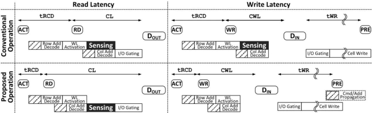
This SMART bank architecture does not increase latency of memory read accesses, because the total amount of time for performingACTandRDremains the same as conven-tional STT-MRAM. As shown in Fig.2.3(left), compared with conventional STT-MRAM, SMART simply reduces the amount of time forACT(tRCD) while increasing the amount of time forRD(CL). On the other hand, as shown in Fig.2.3(right), SMART can decrease latency of memory write accesses. Specifically, compared with STT-MRAM,ACT-WRdoes not consume any time for sensing BLs without affectingCWL, time between the moment at which aWRcommand is sent and the moment at which its first data (DIN) is placed.
In DRAM, the SIO-LIO lines are electrically isolated from the GIO lines, as shown in Fig. 2.1a. This allows DRAM to internally pipeline more than two consecutive RD commands which can be issued at every tCCD interval (typically∼5ns) without waiting for long CL (typically ∼13.75ns), as shown in Fig. 2.1e. SMART, however, has longer
WL Sensing CL WL DRIVER ACT RD BL LBL GIO SA SA SSL SSL CSL CSL GBL DQ MEM CELL BL LBL GIO SA SA SSL SSL CSL CSL GBL DQ BL LBL GIO SA SA SSL SSL CSL CSL GBL DQ tRCD tCCD
(a) Page mode and pipelinedRDcommands
LBL
BL GBL
LBL
Sense Amps Sense Amps
Sense Amps
BL GBL
(b) Enhanced bank architecture
Figure 2.4: SMART page mode and enhanced bank architecture.
read time thantCCDbecauseRDalso senses BLs, as shown in Fig.2.4a. To hide such long sensing time for consecutiveRDcommands, we propose to double the number of LBL and GBL lines, column multiplexers, and SAs, as shown in Fig. 2.4b. The two sensing paths take turns to serve consecutiveRDcommands so that SMART can handle oneRDcommand at everytCCDinterval, as depicted in Fig.2.4a. Our analysis in Sec.2.4.1shows that the cost of doubling the number of sensing paths does not increase the cost of STT-MRAM. In fact, SMART decreases the cost by∼6% because SMART still uses 8×fewer SAs than conventional STT-MRAM.
2.3.2
Benefits
With the bank architecture presented in Sec. 2.3.1, SMART can provide the following notable benefits over conventional STT-MRAM.
Benefit 1: Larger pages and fewer SAs. SMART with a re-defined page mode can give the illusion of providing larger pages but demanding fewer SAs than conventional STT-MRAM. Specifically, anACTcommand of SMART simply asserts a WL to connect every cell in the row to 16,384 BLs, and it is a subsequentRDcommand that selects appropriate 64 BLs and senses them. That is, SMART needs only 64 SAs per bank for 2KB pages whereas conventional STT-MRAM implements 1,024 SAs per bank for 128B pages. Because con-ventional STT-MRAM implements 16×fewer SAs than BLs, it repeatedly consumes long time (tRC= 27.5ns) for accessing the same row but columns which were not selected and sensed by the previousACTcommand. SMART, however, does not consumetRCfor such
Word-line Activation Page Size = 2KB E n e rg y
Bit-line Charging and Sensing Wasted energy Word-line Activation Page Size = 128B E n e rg y
Bit-line Charging and Sensing
Wasted energy Wasted energy Read access granularity Reduced pages in conventional STT-MRAM DRAM SMART Read access granularity Read access granularity Bit-line Charging and Sensing E n e rg y Word-line Activation Page Size = 2KB
Figure 2.5: Relation between page size andACTenergy.
column accesses because it only needs another RDcommand to connect and sense these columns. This can significantly reduce the latency of sequential memory accesses. Note that the SAs in conventional STT-MRAM consume ∼9% of STT-MRAM space based on an adapted version of DRAMSpec [65]. That is, SMART can reduce the space and acti-vation power consumed by SAs to 12.5% of conventional STT-MRAM. This is sufficient not only to negate the cost increased by another read path but also to significantly reduce sensing power and memory access latency, as elaborated below.
Benefit 2: Lower activation power with fewer SAs. ACT energy is a major contribu-tor to total DRAM energy in DRAM. To reduce theACTenergy, DRAM architectures with smaller pages and fine-grained activation have been proposed [19–22]. In contrast, SMART reducesACTenergy while providing larger pages with fine-grained activation at a smaller cost than STT-DRAM. Fig.2.5 illustrates the relationship between page size andACT en-ergy in DRAM, STT-MRAM and SMART. In a DRAM device providing 2KB pages,ACT
ACT RD DOUT tRRD ACT RD DOUT CL tRCD Limited bank interleaving by tRRD ACT RD DOUT ACT RD DOUT CL CL tRCD CL tCCD tRCD Bank interleaving without tRRD restriction
Figure 2.6: Impact oftRRDon bank-level parallelism.
asserts a WL, connecting 16,384 cells to 16,384 BLs. Although we consider higher WL voltage (VP P) than the BL voltage (VDD) and low efficiency of the charge pump to
gener-ate VP P (∼30% [66]), we see that charging/discharging the BLs still dominates the ACT
energy because of the large number of BLs. Since aRDcommand accesses only ∼0.4% (= 64/16,384) of cells in a row, sensing 16,384 BLs for only a fewRDaccesses, referred to as the overfetching problem, wastes a significant amount of energy in DRAM, as shown in Fig.2.5(top).
Benefit 3: Shorter latency with lower activation power.HighACTpower affects not only total memory energy but also overall memory performance. Specifically, simultaneous ac-tivation of multiple rows, each charging/discharging 16,384 BLs, draws a large amount of current. This requires some time to recover from the voltage drop of the power delivery network, which is enforced bytRRD(RAS to RAS delay) andtFAW(four activation win-dow). If there are two read accesses to different banks, the second ACTcommand can be scheduled between the firstACT andRDcommands, but not untiltRRDhas elapsed from the firstACTcommand, as depicted in Fig.2.6(top). tFAWlimits the number ofACT com-mands to four within a tFAWtime window. Therefore, these constraints limit bank-level parallelism and they are imposed on not only DRAM but also other memory technologies. For example, LPDDR2-NVM also definestRRDandtFAW[63].
We plottRRDandtFAWfor various page sizes in Fig.2.7, where the maximum activa-tion current values are determined by a method of prior work [67]. This shows thattRRD
0 2 4 6 8 10 12 14 16 18 20
tR
R
D
[
n
s]
Page Size [Byte]
tRRD (STT-MRAM) tRRD (DRAM) (a)tRRD 0 10 20 30 40 50 60 70 80 90 100tF
A
W
[n
s]
Page Size [Byte]
tFAW (STT-MRAM) tFAW (DRAM)(b)tFAW
Figure 2.7: tRRD and tFAW for various page sizes. tRRD and tFAW for DRAM are obtained from a DDR3 datasheet [4].
andtFAWof conventional STT-MRAM with the page size of 128B are∼6.2nsand∼30ns, respectively. Since a current SA consumes far more power than a voltage SA, STT-MRAM needs longer tRRD than DRAM for the same page size. In contrast, SMART activates 16×fewer SAs and thus consumes less power than conventional STT-MRAM. Note that SMARTACTdoes not consume any sensing power and the recovery time for activating 64 SAs is short enough compared totCCD(∼5ns). Hence, SMART can practically eliminate these two constraints and handle multiple ACT–RDcommands to different banks back to back. This significantly reduces the latency of memory accesses especially for memory-intensive applications. For example, SMART can serve two ACT–RDcommands to two different banks without consumingtRRD, as shown in Fig.2.6(bottom).
Lastly, SMART also consume shorter time and less power than conventional STT-MRAM for memory write accesses. This is because an ACT command of SMART does not consume time and power for sensing which is unnecessary for memory write accesses, whereas conventional STT-MRAM still does.
Benefit 4: Fewer pins and more efficient repair. Unlike conventional STT-MRAM, SMART does not demand any part of a column address withACT, and thus it needs the same number of address pins as DRAM. That is, SMART does not suffer from the column address fragmentation problem discussed in Sec.2.2.2. As discussed in Sec.2.2.2,
repair-MAT Repair Logic MAT SA Repair Logic CS Repair granularity 1 BL 64 BLs 16 BLs Repair flexibility Within a MAT Within a BL group Within a MAT
DRAM
& SMART Conv. STT-MAMRepair @ ACT Repair @ Conv. STT-MAMRD/WR
u v Normal SA Redundant SA 1024 NBLs 4 RBLs 16 NBLs1 RBL SA CS SA CS Total 64 SAs Total 64 RBLs MAT SA Repair Logic CS w SA CS SA CS 16 RBLs 1024 NBLs u v w Normal BL (NBL) Redundant BL (RBL)
(a) Example of various column repair schemes
0% 10% 20% 30% 40% 50% 60% 70% 80% 90% 100% 0 10 20 30 40 50 60 C h ip Y ie ld
Number of redundant BLs per MAT
DRAM & SMART Conv. STT-MRAM @ ACT Conv. STT-MRAM @ RD/WR
(b) Chip yield according to repair schemes
Figure 2.8: Comparison of the three repair schemes.
ing a mat of conventional STT-MRAM is not as efficient and flexible as DRAM because the column address fragmentation problem splits a column address betweenACTandRD. This can significantly increase the cost of repairing mats or decrease the yield of STT-MRAM chips. Fig. 2.8a describes the column repair schemes for DRAM and conventional STT-MRAM. In DRAM (1), we can replace any 1,024 BLs with any 4 redundant BLs in a mat, and we repair a BL with aRDorWRcommand comprising a complete column address [68]. As SMART also exposes a complete column address to aRDorWRcommand, it can adopt the same column repair scheme as DRAM. In conventional STT-MRAM, however, nei-ther aACTcommand nor aRD/WRcommand has a complete column address. This makes repairing BLs far less efficient and flexible than DRAM or SMART.
Consider STT-MRAM with 1,024 BLs per mat andN (= 16) BLs per SA, (i.e, 1,024/N
= 64 BL groups). If we are to repair a BL with ACT(2), we need one redundant BL for everyN BLs (= 64 redundant BLs) asACTcan select only one BL in each BL group. On the other hand, if we are to repair a BL withRDorWR(3), we need to replace the entire BL group including a defective BL with a redundant BL group (= 16 redundant BLs) because RDorWRcan select only BL groups.
We analyze the chip yield for various numbers of redundant BLs in Fig.2.8bwhere we assumed that capacity of a chip is 8Gb, the number of mats is 16,384 in a chip where each
ACT RD DOUT tRCD PRE ACT RD PRE ACT RD ACT RD ACT RD ACT RD DOUT DOUT DOUT DOUT DOUT CL tRAS tRP tRCD CL tRTP tRP tRCD CL tRTP CL tRCD tRCD CL tRCD CL No recovery in STT-MRAM Skipping pre-charge in SMART DRAM
Figure 2.9: Change of row access cycle on row misses.
mat has 512 WLs and 1024 BLs,N is 16 for conventional STT-MRAM, memory defects follow a Poisson distribution [68,69], the target bit error rate (BER) after row repair is10−7 and both DRAM/SMART and conventional STT-MRAM use the same row repair scheme. This shows that conventional STT-MRAM has a lower chip yield than DRAM or SMART for the same number of redundant BLs. In other words, to accomplish the same chip yield (99%) under the same BER (107), conventional STT-MRAM requires 10.7×
more redundant BLs than DRAM and SMART.
Benefit 5: Eliminating precharge commands. To activate another row in the same bank (handle a row-buffer miss), a precharge (PRE) command needs to be sent to DRAM before anACTcommand. Specifically,PREin DRAM consists of two phases: (1) deactivating an asserted WL and (2) initializing BLs beforeACTsenses BLs. (2) also destroys cell states if it is performed before the WL is completely deactivated. Therefore, (1) should be com-pletely done before (2) is started, and the amount of time for (1) and (2) (tRP) increases latency of memory accesses when row-buffer misses occur, as shown in Fig.2.9(top). Fur-thermore, when STT-MRAM follows the same page mode operation as DRAM, it experi-ences more row-buffer misses with smaller pages and thus it pays this penalty more fre-quently than DRAM.
(2) because of the non-destructive nature of its read operation. Moreover, STT-MRAM immediately transfers the cell states sensed by SAs to registers serving as a row buffer (Sec. 2.2.1). This allows STT-MRAM to initialize the BLs and SAs immediately after sensing BLs as part of ACT and reduce tRP. Note that STT-MRAM initializes its BLs by discharging them to VSS. The driving strength of charging BLs is limited to prevent
unexpected changes of cell states (read disturbance) [40,70], but that of discharging BL is not limited. Hence, the amount of time for (2) can be much shorter than DRAM and it is already included intRAS instead oftRP [27,42,50]. This reducestRP of STT-MRAM by the amount of time for (2). Consequently, as shown in Fig. 2.9(middle), STT-MRAM can serve the secondRDcommand faster than DRAM, but it does not reduce or hide the amount of time for (1), still demanding a separate PRE command. In contrast, SMART can overlap the amount of time for (1) (∼3.7ns) with the amount of time to decode a given row address and compare the address with addresses in a row repair table [68] during the early phase ofACTfor the next row (∼4.2ns)4. This allows SMART to completely remove
PREright beforeACT, further reducing the latency to handle row-buffer misses. Note that prior work only reducestRP[42,59] while SMART does not consumetRPat all to handle row-buffer misses.
2.3.3
Discussion
SMART can consume far less space for SAs and redundant BLs than conventional STT-MRAM but more space for another sensing path per bank. Overall, SMART is ∼6% smaller than conventional STT-MRAM (Sec. 2.4.1). We summarize the key differences among DRAM, LPDDR2-NVM, conventional STT-MRAM and SMART in Table2.1
SMART does not increase the latency of serving a single read request or consecutive read requests issued at thetCCDinterval but it still increasesCL. This may increase overall 4In this case, we leverage the∼0.5nsdifference, but some overlap between deactivating the previous WL and activating the current WL is still acceptable because such overlap does not destroy the cell states.
T able 2.1: Comparison with pre vious studies DRAM LPDDR2-NVM [ 38 , 63 ] Con v-Delay [ 27 , 42 ] Con v-Pin [ 24 , 41 ] This w ork (SMAR T) P age size Lar ge (2KB) Small (32B) Small (128B) Small (128B) Lar ge (2KB) Acti v ation ener gy High Medium Medium Medium Extremely lo w Bank-le v el parallelism Limited by tRRD / tFAW Same as DRAM Same as DRAM Same as DRAM No limitation Pin-compatible with DDR Y es Y es (3-phase addressing) Y es (delayed ACT ) No Y es Repair fle xibility High Lo w Lo w Lo w High PRE technique SALP [ 59 ]: Can violate tRP to access dif ferent sub-array No EarlyP A [ 42 ]: Internally perform PRE after the sensing and set tRP =1 No No PRE command and no tRP Need softw are/OS support No Y es, for write operation No No No Highlighted green: good features , highlighted yello w: good, b ut limited , (Con v-Delay and Con v-Pin are the con v entional STT -MRAM designs)
read latency of serving multiple read requests issued at longer intervals thantCCD. How-ever, our evaluation shows that the performance degradation caused by the increasedCL is outweighed by the performance increase by larger pages, higher bank-level parallelism, and lower row-buffer miss latency.
Since a row buffer holds data only for a previously accessed column, SMART cannot compare-before-write when aWRcommand is sent to a different column of the activated row. Comparing data before writing reduces write energy and improves the endurance by not overwriting the same data [27,71]. However, the high endurance of STT-MRAM cells (> 1015) guarantees practically unlimited write operations (Sec. 2.2.1). Moreover, cell
write energy is not a major component in overall write energy. Therefore, such a technique has limited impact on giga-bit scale STT-MRAM (Sec.2.4.3).
Lastly, as this work focuses on re-architecting STT-MRAM for higher performance and lower energy, we do not discuss challenges related to its cells, such as thermal stability, write endurance, and read disturbance in detail [47,70]. Nonetheless, recent studies have demonstrated small 20nm) STT-MRAM cells that can offer fast switching time (sub-10ns) under low write current (sub-10uA), high write endurance (>1015), thermal stability
and read disturbance [72–74].
2.4
Device Modeling
To evaluate DRAM, STT-MRAM and SMART, we take DRAMSpec [65], a detailed tim-ing, power, and area exploration tool which is originally developed for DRAM but can be adapted for other memory technologies such as STT-MRAM. For the baseline DRAM, we consider×8 8Gb DRAM devices. While keeping the same chip floor-plan as DRAM, we adapt the bank architecture and interconnect models to model STT-MRAM and SMART with parameters taken from NVSim [75] and prior work [27,28,32,33,46] and then extrap-olated to 30nmtechnology.
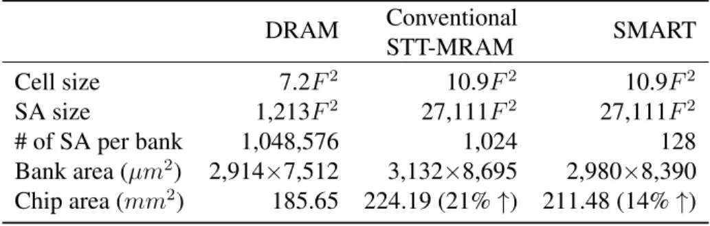
Table 2.2: Area comparison DRAM Conventional STT-MRAM SMART Cell size 7.2F2 10.9F2 10.9F2 SA size 1,213F2 27,111F2 27,111F2 # of SA per bank 1,048,576 1,024 128 Bank area (µm2) 2,914×7,512 3,132×8,695 2,980×8,390 Chip area (mm2) 185.65 224.19 (21%↑) 211.48 (14%↑)
2.4.1
Area Model
We assume a 7.2F2 DRAM cell (2F×3.6F = WL×BL) provided by the DRAMSpec’s
30nm technology model and a 10.9F2 (3F×3.6F) STT-MRAM cell. For conventional
STT-MRAM, we takeN = 16 which is from an industry STT-MRAM chip [27]. Following the JEDEC standard for DRAM, SMART has the same number of rows and columns as DRAM. However, SMART can implement any page size with the number of SAs equal to the number of bits per column access.
We also assume 12 redundant WLs and BLs per mat for DRAM and SMART (default in DRAMSpec) whereas we suppose 32 redundant BLs per mat for conventional STT-MRAM (Sec.2.3.2). Prior work [50] demonstrated the layout area of various SAs for STT-MRAM, but it designed the SAs with a logic technology. Thus, we convert transistor sizes and design rules to those of a memory technology based on the ITRS roadmap to re-estimate the area [76].
We summarize the analyzed area of key memory components in Table 2.2. The total height of the BLSA blocks in DRAM is ∼20% of the total chip height in a 20nm 8Gb DRAM device [77]. Therefore, the number and size of SAs greatly affect the total chip size. SMART has 2×more sensing paths than conventional STT-MRAM, but it consumes
∼6% smaller space because it needs 8×fewer SAs. Albeit SMART uses 1.5×and 21.4×
larger cells and SAs than DRAM, it uses 8,192× fewer SAs. This is because that a bank has 128 sub-arrays and a pair of two sub-arrays shares 16,384 SA in DRAM. SMART is
only 14% larger than DRAM whereas conventional STT-MRAM is 21% larger.
2.4.2
Timing Model
Table. 2.3 summarizes the timing parameters and read access latency of DRAM, con-ventional STT-MRAM and SMART, based on the memory clock frequency of 800MHz. DRAM gives the shortest latency for a single read access because the sensing speed of DRAM is faster than that of STT-MRAM. However, the overall latency of multiple read accesses is not determined not only by the sensing speed but also by other timing parame-ters such astRRD,tFAW,tRASandtRP, especially when different banks and rows need to be accessed.
Table 2.3: Timing and latency comparison
DRAM Conventional STT-MRAM SMART tRCD(clock cycle) 11 17 (1) 8 tRAS(cc) 27 18 (19) 9 tWR(cc) 12 19 (19) 19 tRP(cc) 11 4 (4) 4 tRTP(cc) 6 1 (18) 9 tRRD(cc) 6 5 (5) 1 tFAW(cc) 32 24 (24) 4 CL(cc) 11 8 (25) 17
Latency for single read 22 25 (26) 25
Latency for five reads
- all different banks 54 49 (50) 41
Latency for two reads - same bank, but differ-ent rows
60 47 (48) 42
The numbers in ( ) are for the delayingACTlike comboAS [27,42].
2.4.3
Energy Model
In conventional STT-MRAM, activating fewer SAs reduces the energy consumption of a singleACT command. SMART, however, completely removes sensing energy from ACT
and thus it gives much smaller ACT energy than conventional STT-MRAM, as shown in Table 2.4. Instead, SMART includes the sensing energy in RDand thus theRDenergy is higher than DRAM and conventional STT-MRAM. The conventional STT-MRAM has the lowestRDenergy because of the reduced read path. Besides, STT-MRAM consumes higher WRenergy than DRAM because of higher write current per cell. However, considering the energy consumption to transfer data across the chip through long interconnects, the impact of the cell write energy on the total write energy is limited.
Table 2.4: Energy and current comparison
DRAM Conventional
STT-MRAM SMART
ACT(nJ) 1.28 0.45 0.09
SingleRD(nJ) 0.27 0.26 0.31
SingleWR(nJ) 0.28 0.35 0.34
Energy for 8B read (nJ) 1.54 0.71 0.39
Energy for 2KB read (nJ) 69.99 86.56 78.19 Energy for 8B write (nJ) 1.55 0.81 0.43 Energy for 2KB write (nJ) 72.79 96.80 87.40
IDD0(mA) 67 64 43 IDD2P(mA) 14 17 16 IDD2N(mA) 36 39 38 IDD3N(mA) 51 39 38 IDD4R(mA) 122 121 127 IDD4W(mA) 122 132 131 IDD5(mA) 245 -
-Table 2.4 shows the dynamic energy consumption of a single memory device for a single column (8B) request and a single page (2KB) request. If all columns in a page are accessed, STT-MRAM consumes more energy because of its inherent higher sensing and cell write energies. However, a single read/write access in STT-MRAM consumes less energy than DRAM because of the lowACTenergy consumption. Comparing the two STT-MRAM’s energies, SMART is more energy-efficient in all cases. This is because there is no wasted energy for the single column access and there are fewer ACT commands for the 2KB access. In addition, because SMART does not include sensing energy in write
requests, the gap between the two STT-MRAM designs in a 2KB write is larger than that in a 2KB read.
IDD2P is the power-down current and it is close to the sum of total transistor leak-age. Thus, IDD2P is usually proportional to the total transistor width under the same technology. For simplicity, we increase IDD2P of STT-MRAM linearly with chip size. IDD2Nand IDD3N are background current under precharge-standby and active-standby, respectively. The difference between IDD2P and IDD2N mainly results from the ad-dress/clock buffer current components. Thus, we assume the same increment for STT-MRAM’s IDD2N. However, IDD3N stems from DRAM’s unique leakage component. When a row in a bank is activated, 32,768 BLs are fully charged or discharged, whereas all BLs are precharged to VDD/2 level when the row is deactivated. If the BL length is
512, then 16,777,216 cells are connected to the 32,768 BLs. The increased voltage differ-ence between BL to a cell transistor increases leakage current, which is mostly GIDL and junction leakage current [78]. Because of this large number, small leakage current changes cause huge increases in IDD3N. However, the BL/SL condition of STT-MRAM is differ-ent from that of DRAM during active-standby, because BLs and SLs are always discharged except during sensing and writing. Therefore, we assumeIDD3Nis the same asIDD2Nin STT-MRAM.
2.5
Evaluation
2.5.1
Evaluation Methodology
We evaluate SMART using MARSSx86 [79] and DRAMSim2 [80]. The configured system for the evaluation is shown in Table2.5. Power-down mode is enabled to minimize standby power when there are no pending requests in the memory controller.
We employ two benchmark suites: SPEC2006 [82] and STREAM [3]. For multi-core simulations, multi-program workloads are composed as shown in Table2.6.
Misses-per-Table 2.5: Default system configuration Component Specification
Processor single and quad core
Last Level Cache 2MB-8 way (single), 4MB-16 way (quad) Memory Controller FR-FCFS [81], open-page, Ch:Ra:Ro:Ba:Co Memory System 8GB single rank/ch (8Gb x8-DDR3L-1600)
kilo-instructions (MPKI) increases from mix1 to mix9. For all workloads, one billion in-structions are simulated in their region of interest. In our evaluation, there are two con-ventional STT-MRAM designs with the shared SA structure: Conv-Pin and Conv-Delay. Conv-Pin emulates the designs proposed in [24,41]. However, they have no consideration for the expanded address pins which result from the shared SA structure and are not com-patible with JEDEC DDR. On the other hand, Conv-Delay internally delays the activation instead of increasing pin count [27,42].
Table 2.6: Workloads for multi-core simulations Workload Application list
mix1 bzip, povray, astar, libquantum
mix2 hmmer, sjeng, xalancbmk, libquantum mix3 gobmk, h264ref, astar, lbm
mix4 povray, omnetpp, soplex, lbm mix5 sjeng, xalancbmk, mcf, stream scale mix6 h264ref, povray, hmmer, lbm
mix7 bzip, omnetpp, stream copy, stream scale mix8 gobmk, milc, stream add, stream copy mix9 hmmer, mcf, stream triad, stream add
2.5.2
Performance
In SMART, we strive to implement large pages (2KB) with low cost. Memory performance is affected by row buffer hit rate and page size. Both DRAM and SMART can implement 2KB pages, while the conventional STT-MRAM designs can implement only 128B pages. The row buffer hit rates are shown in Fig.2.10. SMART has a row hit rate within 1% of
0 20 40 60 80 100 H it R at e [ % ]
DRAM Conv - Pin Conv - Delay SMART
Figure 2.10: Row hit rate in various workloads.
DRAM’s. However, both conventional designs have significantly lower hit rates, especially in STREAM workloads. Although all designs show low hit rate in a few workloads, the designs with the larger pages still perform better.
Fig.2.11shows the overall read latency distribution of the three devices under the mix6 workload. DRAM has a long tail latency because of refresh, but STT-MRAM has a short tail. In the Conv-Pin, we clearly observe two peaks in its distribution corresponding to read latency under row hits and misses. In SMART, there is no clear second peak because row misses are serviced faster and their read latency is partially overlapped with read latency under row hits. Although SMART has no data in 10∼19 cc range due to its long CL, it mostly falls within 30∼39 cc, implying that it is neither too quick nor too slow. DRAM also has most of its latency within 30∼39 cc, but its long tail negatively affects the overall latency. The average read latency of DRAM, Conv-Pin, and SMART is 52.6, 57.9 and 47.1 cc, respectively.
Fig.2.12shows system IPC improvement over DRAM. Conv-Pin and Conv-Delay de-grade IPC on average by 3.7% and 4.3%. For some memory intensive workloads IPC degrades more than 30%. The biggest drawback in conventional STT-MRAM designs is the small page size. A substantial drop in row hit rate as compared to DRAM (e.g, bwaves, sphinx3 and STREAMs) significantly degrades their IPC. For workloads with similar row hit rate (e.g, lbm and milc), IPC is better than DRAM due to the removed refresh and
![Figure 1.3: DRAM scaling trend [1].](https://thumb-us.123doks.com/thumbv2/123dok_us/1368018.2683197/13.918.282.690.114.337/figure-dram-scaling-trend.webp)


![Figure 2.7: tRRD and tFAW for various page sizes. tRRD and tFAW for DRAM are obtained from a DDR3 datasheet [4].](https://thumb-us.123doks.com/thumbv2/123dok_us/1368018.2683197/33.918.227.732.114.374/figure-trrd-tfaw-various-sizes-dram-obtained-datasheet.webp)